CSSE2010 — Week 8 Notes
Lecture 15 — Flow of Control
Back to assembly, to fill in the two things a program needs beyond straight-line code: branches and jumps, which is where the AVR’s S flag and the signed/unsigned pairs of branch instructions get explained properly, and procedures, which is where the stack enters. The last part opens the next topic, the AVR’s timer/counters, which Lecture 16 takes up. The evergreen notes are avr-branches-and-jumps, procedures-and-the-stack and avr-timers-and-counters.
Outline
- Flow of control
- Branching
- Procedure Calls
- Use of stacks
- Introduction to AVR Timer/Counters
Background
Three things are assumed from here on: the Atmel AVR CPU (the ALU, general purpose and special purpose registers); the main hardware components of the ATmega324A/ATmega328 microcontroller (AVR CPU, Data Memory, Program Memory, GPIO Ports, Timers/Counters, PWM, Communication Interfaces etc); and AVR assembly language instructions.
The course roadmap has four boxes: AVR Assembly language ⇒ AVR C programming ⇒ ALU Operations ⇒ Interaction with I/O. The course does not walk the row left to right. The control-flow instructions here are a step back into assembly, and the timers at the end are the start of the I/O box.
Flow of control
Flow of control is the sequence that instructions actually get executed in. It is linear (i.e. successive instructions) unless there are branches/jumps, procedure calls, etc.
Plot the program counter against time. Linear flow is a straight rising line: the instructions run one after another, and every fetch-decode-execute (FDE) cycle does PC ← PC + 1. Non-linear flow, the typical case, is the same line broken by jumps: a run, then a drop back (a jump to a lower address) or a rise (a jump forward) at each break. A small program with such breaks:
main:   ...
        ...
        call TEST
PING:   ...
        BREQ ABL
TEST:   ...
        ...
        call PING
ABL:
call TEST jumps down to TEST:. Three labels, two calls and a conditional branch: every kind of non-linearity named below is in those nine lines. Figure 1 draws what the program counter does.
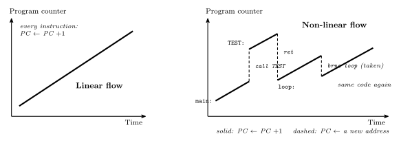
Figure 1: The program counter against time. Left: straight-line code, where every fetch-decode-execute cycle adds one to the PC and the plot is a line of constant slope. Right: the same plot for code with a procedure call, its return and a backward conditional branch. Between the breaks the slope is still one instruction per cycle; each break is a single instruction that loads a new value into the PC instead of the next address. A call jumps forward to the procedure, ret drops back to the instruction after the call, and a taken backward branch drops back to a label above it, which is what a loop looks like. The rises and drops are the only thing that separates the two plots: control flow is the PC being overwritten.
What breaks sequential execution
Most instructions result in the PC being incremented (sequential execution), i.e. PC ← PC + 1, as in the fetch-decode-execute-cycle. Instructions are not executed sequentially when there are:
| ① Branches | conditional |
| ② Jumps | unconditional |
| ③ Procedures | function calls |
| ④ Interrupts / Traps |
The first three are the three sections that follow, in that order. Interrupts are in Lecture 17 (2026-09-21-interrupts; the mechanism is in polling-and-interrupts).
Branches
- AVR branch instructions are typically conditional.
- They are useful in implementing if-else and loops in assembly language.
breqandbrneare the two met so far (2026-09-03-instruction-set-architecture-part-2, and the compare-then-branch figure in avr-program-structure).- For a comparison such as greater than or equal to, the instruction used depends on whether the numbers being compared are unsigned or signed (two’s complement).
breq/brne only ask equal or not, and equality means the same thing for signed and unsigned bytes. Greater than does not: 1111 1111 is 255 unsigned and −1 signed, so whether it is greater than 0000 0001 depends on which you meant, and the machine cannot know. Hence two instructions.
Branches — AVR assembly example
cp r5, r6 computes r5 − r6 and updates the status flags N, Z, C, V and S. Take this pseudo code on two registers:
r5, r6
if (r5 ≥ r6)
    ⋯    (the if part)
else
    ⋯    (the else part)
In the assembly that implements it, the if body goes under the IF: label and the else body goes in the lines directly after the branch:
        cp   r5, r6
        brge IF
        ...              ; the else part
        ...
        jmp  EXIT
IF:     ...              ; the if part
        ...
EXIT:   nop              ; "no operation"
Figure 2 lays the two side by side.
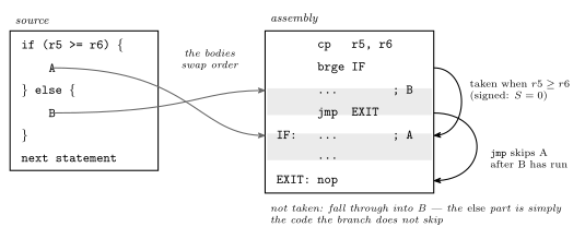
Figure 2: How an if … else becomes assembly. The compare sets the flags; the conditional branch reads them and jumps to the if part when the condition holds. Because a branch can only jump somewhere, the code that runs when the condition fails has to be the code the branch skips over — so the else part sits directly after the branch, ends in an unconditional jmp past the if part, and the if part lives under a label further down. The two bodies end up in the opposite order from the source, which is the thing to expect when reading assembly back into C. EXIT carries a nop only so that the label has an instruction to name; anything that follows the statement would do.
If S = 0, brge makes the jump. There are three cases where it has to, each placed on the signed number line:
| Case | Number line | Flags |
|---|---|---|
① r5 > r6 |
0, r6, r5 in that order, both to the right of zero |
N = 0, V = 0 |
② r5 = r6 |
N = 0, V = 0 | |
③ r5 > r6 |
r6 far to the left, r5 far to the right, and r5 − r6 wrapping round past 127 |
N = 1, V = 1 |
In all three S = N ⊕ V = 0, so brge jumps in all three, which is what greater than or equal requires. Case ③ is the one that justifies the S bit: r5 is a large positive and r6 a large negative, so r5 − r6 is bigger than 127 and overflows into a result whose top bit is 1. The N bit therefore says negative, which is wrong; the V bit says but that sign is an overflow artefact; and their XOR cancels the two to give the true sign. Figure 3 draws the three, and a fourth case, r5 < r6, where the branch must not be taken.
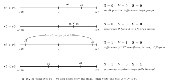
Figure 3: Why a signed comparison tests S and not N. Each panel is the signed number line of an 8-bit register, \(-128\) to \(127\), with the two operands of cp r5, r6 marked and the flags the subtraction sets. In the top three cases \(r5 \ge r6\) and brge must jump; in the first two the difference fits and N alone would do. In the third the true difference is larger than 127, the 8-bit result wraps to a negative pattern, and N reports the wrong sign — but the overflow flag V is set at the same time, and S = N \oplus V corrects it back to 0. The bottom panel is the case the branch must not take: \(r5 < r6\) gives a genuinely negative difference, N = 1 with V = 0, so S = 1. Reading S gives the right answer in all four; reading N fails in the third.
AVR “S” status bit
Two status bits met earlier:
- N bit = negative (1 if the sign bit of the result is 1)
- V bit = two’s complement overflow
The AVR also has the S bit: S = N ⊕ V, the sign bit corrected for overflow. If overflow happens, the sign bit will be wrong, so instead of checking the N bit, check the S bit.
S has been in the status register since Lecture 10 (avr-architecture); this is what it is for. It exists so that a signed less than is one flag test rather than two.
Branch instructions
Each conditional branch tests one status bit for one value:
| Branch if status bit is equal to | C | N | V | S = N⊕V | Z |
|---|---|---|---|---|---|
| 0 | brsh (= brcc) |
brpl |
brvc |
brge |
brne |
| 1 | brlo (= brcs) |
brmi |
brvs |
brlt |
breq |
Ten instructions, one per flag per value. Two of the columns are the comparisons that matter here:
| unsigned | brsh — same or higher |
brlo — or lower |
| signed | brge — greater than or equal |
brlt — lower than |
A worked example: r5 = 1111 1111, r6 = 0000 0001. Read as unsigned, cp computes 255 − 1, which is positive, so brsh is the branch taken. Read as signed, cp computes −1 − 1, which is negative, so brlt is the branch taken. Same two registers, same cp, same flags — and one branch says r5 is higher, the other says r5 is less. Both are right. The unsigned pair reads C, because an unsigned subtraction that needs a borrow is exactly one whose result went below zero; the signed pair reads S, for the reason worked through above. The programmer chooses the instruction and thereby declares what the bits meant, the same decision as lsr versus asr in 2026-09-03-instruction-set-architecture-part-2. Full table and the loop idioms in avr-branches-and-jumps.
Jumps
The AVR has three jump instructions:
jmp label — absolute jump, 32-bit instruction, 3 cycles |
label is a 14-bit address |
rjmp label — relative jump, 16-bit instruction, 2 cycles |
label becomes an offset, − or + up to 2048 cells |
ijmp — indirect jump, 16-bit instruction, 2 cycles, jump target is given in Z register |
Why two sizes. jmp carries the destination as a full program-memory address, and an address into the ATmega324A’s 16 K-word flash needs 14 bits — more than fits in a 16-bit instruction word alongside the opcode, so jmp takes two words (avr-instructions on instruction encoding). rjmp instead carries a signed offset from the current PC, 12 bits of it, so it can reach ±2 K words — 2048 cells either way — in a single word and one cycle less. Almost every jump in a small program is within that range, which is why the labs’ template uses rjmp for its main loop. ijmp takes the address from Z, the pointer register of addressing-modes: the destination is a value, computed at run time, rather than a label fixed at assembly time.
Procedures
A procedure is a group of instructions that performs some task.
- It may have operands (arguments or parameters).
- It may produce result(s).
- It can be invoked (called) from multiple places in a program, even from within itself: a recursive procedure.
- After invocation, control returns to the statement after the call.
- Good use of procedures helps structure a program well.
- Other names: subroutine, function (C, Python), method (Java).
The shape of a call:
main:   ...
        ...
        call TEST      ; args ?
        [xxx]          ; the instruction after the call

TEST:   ...
        ...
        ret            ; returns results ?
call TEST jumps down to TEST:, and ret jumps back up to [xxx], the instruction after the call. The two questions in the comments are among the procedure issues below.
Call instructions
The AVR has three call instructions:
call label |
direct subroutine call, 4 cycles, 32-bit instruction |
rcall label |
relative subroutine call, 3 cycles, 16-bit instruction |
icall |
indirect call, 3 cycles, 16-bit instruction |
The same three flavours as the jumps — absolute, relative, indirect — each one cycle longer than its jump, which is the cost of saving the return address.
Procedure issues
Procedures raise three questions:
- After a procedure finishes, control returns to the statement after the call. How does the procedure know where to return to?
- How are operands specified (i.e. arguments passed)?
- How is the result returned?
The first takes the most answering. The other two are answered together, briefly, once the stack is in place.
Return address
There are three places the return address could be stored:
| Option | Problem |
|---|---|
| A single fixed memory address or register for all procedure calls | procedures can’t call other procedures |
| A memory location per procedure | doesn’t allow for recursion |
| A stack |
The second option fails for a procedure that calls itself:
main:   ...
        call TEST
        [xxx]
TEST:   ...
        call TEST
Two calls of TEST are live at once, so two return addresses must be kept at once; one slot per procedure holds one. Two return addresses kept one above the other are already a stack.
Each option fails on the next level of nesting. A single slot works until a procedure calls a procedure — the second call overwrites the first’s return address and main is never returned to. A slot per procedure works until a procedure calls itself. A stack works for any depth, because every call pushes and every ret pops, so the return address that comes off is always the one that went on most recently, which is the innermost call still running. Figure 4 draws the mechanism.
Procedure call — use of stack
call pushes onto the stack and ret pops from it:
main:   ...
        ...
     →  [xxx]  call TEST     ─── push ──→   the stack
TEST:   ...
        ...
        ret               ←── pop  ───
The stack is a region of data memory, at the opposite end from the data that memory already holds. The pushed cell is xxx, with SP pointing at it, and each cell is 8 bits wide. A stack frame stacks three things together: xxx / args / results.
The stack pointer is the register that keeps track of the top of the stack. On the AVR it is SPH:SPL, two I/O registers for a 16-bit stack pointer.
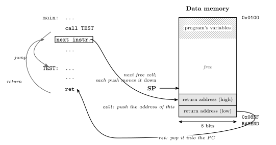
Figure 4: What call and ret do with the stack. The stack is a region at the top of data memory, addressed downward: it starts at RAMEND and grows toward lower addresses as things are pushed, so it approaches the program’s variables from above. call TEST pushes the address of the instruction after itself — the return address — and moves the stack pointer down; ret pops that address back into the PC and moves the pointer up. On the AVR each cell is one byte and the PC is wider than a byte, so a return address occupies two cells and SP moves by two. The pointer itself lives in two I/O registers, SPH:SPL, and must be set to RAMEND before the first call, or the first push lands wherever the reset value happens to point.
Why the stack is at the top. Data memory’s SRAM runs from 0x0100 to 0x08FF (memory-models); the program’s variables are allocated from the bottom of that region upward, so the stack is started at the very top, RAMEND, and grows down toward them. The two can grow toward each other for as long as the memory lasts, and neither needs to know in advance how much the other will use.
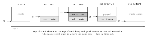
Figure 5: The stack through a nested call. Five snapshots of the stack region, one per event, for main calling TEST and TEST calling PING. Each call pushes one return address on top of whatever is there; each ret pops the top one, which is always the return address of the call made most recently and not yet returned from. After the inner ret the outer return address is exactly where the outer call left it, so TEST returns to main correctly even though another call happened in between. A single fixed slot would have been overwritten by the second push; this is the property that a per-procedure slot lacks for recursion and a stack has for any depth.
Assembly programs — stack initialisation
Assembly language programs must initialise the stack before using it:
.def temp=r16
    ldi temp,low(RAMEND)
    out SPL, temp
    ldi temp,high(RAMEND)
    out SPH, temp
Four instructions that go at the top of RESET: in every program that will ever call anything. RAMEND is the assembler’s name for the last SRAM address, 0x08FF on the 324A; low() and high() split it into its two bytes because SPL and SPH are two 8-bit I/O registers and there is no 16-bit out. This is the line the Lab 10 template was missing (avr-program-structure) — it did not need one, because nothing in it called a procedure. In C the compiler emits this for you; that is one of the things main costs.
Procedure call — arguments and results
There are two ways to pass arguments to a procedure and to return results from it:
- use registers
- or use the stack
Registers are the fast answer for a few small values — put the argument in r24, say, and the procedure reads it from there — and the AVR C compiler does exactly that for the first few arguments of a function. The stack is the general answer: the caller pushes arguments before the call, the procedure finds them just above the return address, and results can go back the same way. That is the stack frame — xxx / args / results stacked together. Conventions for which registers and in what order are in procedures-and-the-stack.
AVR timers/counters
The ATmega324A has three timer/counter blocks on its block diagram: 8-bit T/C 0, 16-bit T/C 1 and 8-bit T/C 2. The diagram also has a fourth, 16-bit T/C 3, but that one is on the larger family members, not the 324A (avr-architecture). On the pinout, six pin functions belong to the timers: OC0A and OC0B on PB3 and PB4, OC1B and OC1A on PD4 and PD5, OC2B and OC2A on PD6 and PD7. These are the output compare pins, one pair per timer, and they are where a timer reaches the outside world; Lecture 16 uses them.
- A counter is a binary up/down counter clocked on some event.
- A timer is a counter clocked by a regular clock.
So the hardware is one thing — a counter of the kind built in [counters], now wide and in silicon — and timer versus counter is only a statement about where its clock comes from. Clock it from a pin and it counts events; clock it from the system clock and, since every tick is the same length, its count is elapsed time.
ATmega324A — timer/counter clock sources
The three timer/counters:
| Width | Clock sources | |
|---|---|---|
| 0 | 8 bit (0 to 255) | STOPPED, CLK, CLK/8, CLK/64, CLK/256, CLK/1024, external pin rising edge, external pin falling edge — CLK = system clock |
| 1 | 16 bit (0 to 65535) | the same list |
| 2 | 8 bit (0 to 255) | STOPPED, CLK, CLK/8, CLK/32, CLK/64, CLK/128, CLK/256, CLK/1024 — CLK = system clock or external oscillator |
CLK is 8 MHz, the system clock the lab boards run at. Timer 2 trades the two external-pin inputs for two extra divisors and can run from a separate crystal on the TOSC1/TOSC2 pins, the port-C pins that avr-io-ports noted were broken out separately on the block diagram; that is what makes it the real-time-clock timer.
Clock prescaling
Take four clocks: CLK, CLK/2, CLK/4 and CLK/8. The counter advances on the rising edges, and over the same stretch of time there are four on CLK, two on CLK/2, and one each on /4 and /8. An 8-bit count climbs a staircase from 0 to 255, and an event happens when the count reaches the top. The staircase is steepest for CLK and shallower for each further division. Drawn as a sawtooth, the count has short ramps of period T for CLK, and long ramps spanning eight clock periods for CLK/8.
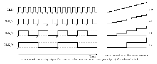
Figure 6: What a prescaler does to a timer. The counter advances by one on every rising edge of its selected clock; dividing the system clock by \(N\) stretches every count to \(N\) system-clock periods. The staircase under each track is the resulting count against the same time axis: at CLK the timer climbs eight steps in the window shown, at CLK/8 it climbs one. A full sweep from 0 to 255 therefore takes \(256 \cdot N\) system-clock cycles, and the prescaler is the coarse control over how long a timer’s period is, before the compare registers give fine control. At 8 MHz the sweep is 32 µs with no prescaling and about 33 ms at CLK/1024.
The prescaler is a chain of flip-flop dividers ([counters] — a ripple counter’s stages are exactly CLK/2, CLK/4, CLK/8, …), and the timer is handed one tap of it. The staircases are the point: the same 0-to-255 sweep takes eight times as long on CLK/8 as on CLK, and 1024 times as long on CLK/1024. At 8 MHz that is the difference between 32 µs and 33 ms per sweep, which is the range that makes an 8-bit counter useful for both microsecond and human-scale timing.
Clock selection
The clock source for timer/counters 0 and 1 is chosen by a multiplexer with seven inputs: 0 (clock stopped), CLK, CLK/8, CLK/64, CLK/256, CLK/1024, and the external source, which enters twice, once directly and once through an inverter so that either edge can be chosen. Three select lines pick the input; the output is the counter clock source.
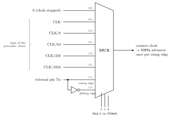
Figure 7: The clock selection multiplexer in front of each timer/counter. Eight inputs, three select bits: the CSn2:0 field of the timer’s control register picks one, and a code of 000 selects a constant 0, which is how a timer is stopped without any separate enable. Five of the inputs are taps of the prescaler chain. The external pin Tn enters twice, plain and inverted, so that the counter can advance on whichever edge the application wants; choosing one of those two codes is what turns the timer into an event counter. The select codes are the ones the control register uses for timers 0 and 1; timer 2 has the same shape with the two external inputs replaced by extra prescaler taps.
Choosing an input is one three-bit field in a control register, CS02:0 for timer 0 and CS12:0 for timer 1; the codes are in the figure and in avr-timers-and-counters, and Lab 12 sets them from C. What happens when the timer counts — output compare, the modes, and PWM — is Lecture 16, 2026-09-17-pulse-width-modulation.
See also
- avr-branches-and-jumps — the ten conditional branches, signed versus unsigned,
jmp/rjmp/ijmp, and theif/loop idioms - procedures-and-the-stack —
call/ret, the return address,SPH:SPL,RAMEND,push/pop, passing arguments - avr-timers-and-counters — the three timer/counters, their registers, clock sources and modes
- avr-architecture — the status register, and
S = N ⊕ V - avr-program-structure — labels, the template, and compare-then-branch
- avr-instructions · addressing-modes · memory-models · [counters] · fetch-decode-execute-cycle
- 2026-09-03-instruction-set-architecture-part-2 — Lecture 12, where
breq/brnewere introduced - 2026-09-17-pulse-width-modulation — Lecture 16 · week8-lab-avr-c-programming — Lab 11 · week8-lab-avr-timers — Lab 12
Lecture 16 — Pulse Width Modulation
The timer/counters introduced at the end of Lecture 15 (2026-09-14-flow-of-control), now put to their main use: generating a pulse-width-modulated signal on a pin, entirely in hardware, so that a digital output can behave like an adjustable analog one. The first part completes the timer material: what a timer is for, which pins it owns, which registers configure it, and its three modes of operation. The rest is PWM itself and the two Fast PWM modes of timer/counter 0. The evergreen notes are avr-timers-and-counters and pulse-width-modulation.
Timer/counters — the three jobs
The block diagram has three timer/counter blocks that matter, numbered 0, 1 and 2; the T/C 3 block is not used (avr-architecture).
An 8-bit timer counting up from 0 at the 8 MHz system clock with no prescaling takes
\[T = \frac{255}{8 \cdot 10^{6}} = 30\ \mu\text{s}\]
This is rounded down from the 32 µs the arithmetic gives (\(256 / 8\,\text{MHz} = 32\ \mu\text{s}\) for the full 256 counts). It is the shortest period the timer can produce, and every other period comes from lengthening it.
A timer/counter is for three things:
- Timing, e.g. toggling an LED every 10 ms. The count climbs from 0 to 255 again and again, driven by the 8 MHz clock. A compare value in OCR, say 128, is crossed once per sweep, halfway up. The crossing is a regular event, and a pin can be driven high (1) or toggled on it.
- Counting an external signal. Each step is an external pulse, not a clock tick. With OCR at 100, the crossing means 100 pulses have arrived.
- Pulse width modulation (PWM): a pulse train on a pin.
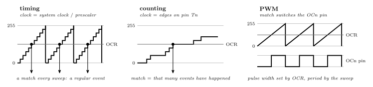
Figure 8: The three jobs of a timer/counter, all built from the same two parts: a count that climbs, and a compare register that marks a value on the way up. Timing: the count is driven by the system clock, so each sweep takes a fixed time and the compare match is a regular event, good for toggling a pin or an LED every so many milliseconds. Counting: the count is driven by edges on an external pin, so the match means a fixed number of events has occurred. PWM: the match is used to switch an output pin partway through every sweep, so the pin carries a pulse whose width is set by the compare value. The hardware does all three without the CPU touching the count.
Timer/counters — separate hardware, configured through I/O registers
A timer/counter:
- can be used to perform actions with pre-defined timing, e.g. do some action every 100 ms;
- can be used to generate PWM;
- can be used to count pulses (logic transitions on a given pin);
- is separate hardware to the CPU;
- is tied to particular pins on the microcontroller. Configuring the timer/counter changes these pins from their default GPIO operation to timer/counter operation;
- is configured by reading and writing I/O registers:
| Register | Kind |
|---|---|
| Timer/Counter register | data: the current value of the count |
| Control registers | control |
| Output compare registers | control |
| Interrupt registers | interrupt |
Every I/O register met so far is one of the same three kinds:
\[\text{I/O reg} \leftarrow \begin{cases} \text{data} & (\texttt{PORT}, \texttt{PIN}, \texttt{TCNT}) \\ \text{control} & (\texttt{DDR}, \texttt{OCR}, \texttt{TCCR}\ldots) \\ \text{interrupt} & (\texttt{TIMSK}, \texttt{TIFR}\ldots) \end{cases}\]
A timer is another peripheral configured through I/O registers, exactly like a port. TCNT is the timer’s PIN, the value you read. TCCR and OCR are its DDR, how it is set up. The interrupt registers are new and are covered in Lecture 17 (2026-09-21-interrupts, avr-interrupts). Separate hardware is the important property: once configured, the timer counts, compares and drives its pin with the CPU doing nothing, which is what makes hardware PWM free.
Timer/counters — the pins
Pins 1–8, at the top left of the pinout, are GPIO port B. Six pins carry the output-compare functions:
| Timer | Pins |
|---|---|
| 0 | PB3 = OC0A, PB4 = OC0B |
| 1 | PD5 = OC1A, PD4 = OC1B |
| 2 | PD7 = OC2A, PD6 = OC2B |
Each timer has two compare units, A and B, each with its own register and its own pin. The two give two independent match events per sweep of one counter. With OCR0A = 200 and OCR0B = 128, timer 0’s count from 0 to 255 crosses both values on every sweep, and each crossing is its own match.
AVR timers/counters summary — ATmega324A
| Timer/Counter 0 | Timer/Counter 1 | Timer/Counter 2 | |
|---|---|---|---|
| Pins | PB3 (OC0A) & PB4 (OC0B) | PD5 (OC1A) & PD4 (OC1B) | PD7 (OC2A) & PD6 (OC2B) |
| Width | 8-bit (counts to 255) | 16-bit | 8-bit |
| Supports PWM | ✓ | ✓ | ✓ |
| Modes of operation | Normal, CTC, Fast-PWM, phase correct PWM | Normal, CTC, Fast-PWM, PC-PWM and PFC-PWM | Normal, CTC, Fast-PWM and phase correct PWM |
| Clock prescaler (\(PRE\)) | No clock, F, F/8, F/64, F/256, F/1024 | No clock, F, F/8, F/64, F/256, F/1024 | No clock, F, F/8, F/32, F/64, F/128, F/256, F/1024 |
| I/O registers | TCNT0 (data); TCCR0A, TCCR0B, OCR0A, OCR0B (control); TIMSK0, TIFR0 (interrupt) |
TCNT1H, TCNT1L; TCCR1A, TCCR1B, TCCR1C; OCR1AH, OCR1AL, OCR1BH, OCR1BL; TIMSK1, TIFR1 |
TCNT2; TCCR2A, TCCR2B; OCR2A, OCR2B; TIMSK2, TIFR2 |
The three modes that matter:
| Mode | Behaviour |
|---|---|
| Normal | the count climbs from 0 to 255 and wraps to 0. It runs freely; a compare value (say OCR = 128) is just a marker on the way |
| CTC — clear on compare | the count resets when it reaches OCR, so the compare value becomes the top of the count |
| PWM | the output is a pulse train |
Timer 1 is 16 bits wide, so every one of its data registers is a pair of bytes with H and L suffixes, and it has a third control register, TCCR1C. Timers 0 and 1 have the same prescaler list. Timer 2’s list adds F/32 and F/128, the two extra taps met in Lecture 15. The register-by-register detail, and Lab 12’s walk through TCCR1A/B/C, are in avr-timers-and-counters and week8-lab-avr-timers.
Pulse width modulation (PWM)
PWM is varying the duty cycle of a periodic pulse. The duty cycle is the percentage of time that the signal is on (high):
\[\text{duty cycle} = \frac{T_{ON}}{T} \cdot 100\%\]
The pulse train switches between 5 V and 0. \(T\) is one full period, in seconds, and \(T_{ON}\) is the high part of it. The frequency is \(f = 1/T\), in Hz. At the same period, a duty cycle of 0 % is flat low, 25 % a narrow pulse, 50 % a square wave, 75 % a wide pulse and 100 % flat high.
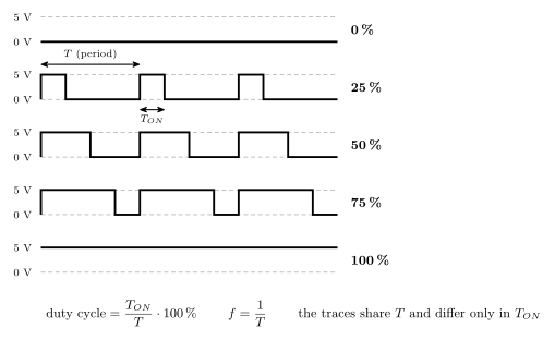
Figure 9: One period of a PWM signal and the two numbers that describe it. The period \(T\) is fixed and sets the frequency \(f = 1/T\); the on-time \(T_{ON}\) is the part of each period the output spends high. Their ratio is the duty cycle. The five traces have the same period and differ only in \(T_{ON}\): from 0,% (never high) through a square wave at 50,% to 100,% (never low). Modulating the pulse width means moving \(T_{ON}\) while leaving \(T\) alone, which is exactly what changing a compare register does.
PWM — average value
If the periodic pulse is “fast enough”, the signal looks like its average value. The average rises with the duty cycle: the 75 % waveform has a higher average than the 50 % one, and the 50 % one a higher average than the 25 % one. So PWM can be used to control the average voltage delivered to a load, for example to control the speed of a DC motor.
The average over one period, for a 5 V pulse:
\[V_{avg} = \frac{\int_0^{T} v(t)\,dt}{T} = \frac{\int_0^{T_{ON}} 5\,dt}{T} = \frac{T_{ON}}{T} \cdot 5 \;\propto\; \text{duty cycle}\]
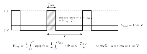
Figure 10: Why a PWM signal has an average, and why it is proportional to the duty cycle. The average of any periodic voltage is the area under one period divided by the period. For a pulse the area is a rectangle, \(5,\text{V} \times T_{ON}\), so dividing by \(T\) leaves \(5,\text{V} \times T_{ON}/T\): the supply voltage scaled by the duty cycle. A load that cannot follow the individual pulses — a motor’s inertia, an LED as seen by the eye, a loudspeaker cone — responds to this average and not to the pulses, which is how a pin that is only ever at 0 V or 5 V delivers 1.25 V.
Fast enough means the load has to be slow compared with the period: a motor’s inertia, a lamp’s thermal mass, the eye’s persistence, or an explicit low-pass filter. If the period is long enough for the load to follow the pulses, it sees pulses. So the PWM frequency is chosen for the load, and then the duty cycle is the only thing varied.
PWM — an average that changes over time
The pulse width can be varied so that the “average value” changes over time. A train of pulses whose widths grow and shrink has an average that follows a sine wave, a sine tone: the pulses are wide at the peak and narrow at the trough. Vary \(T_{ON}\) smoothly from period to period and the average traces out whatever waveform you like; filter off the pulses and that waveform is what comes out. This is how PWM generates audio.
Uses of PWM
PWM is useful for generating signals that look analog from a purely digital source. It can be used for:
- varying the brightness of lights/LEDs (e.g. fading)
- motor control (variable speed)
- generating audio (with appropriate filtering)
The AVR has no digital-to-analog converter; PWM plus the load’s own filtering is how it gets an analog-looking output.
LED brightness fading
Take two pulse trains driving an LED, one with a large duty cycle and one with a small one. Each has its own \(V_{avg}\), and the one with the large duty cycle has the higher \(V_{avg}\). Brightness rises with \(V_{avg}\), so it gives the brighter LED. A wider pulse means a higher average current, and the eye — the low-pass filter in this case — sees a brighter LED. Fading is ramping the duty cycle.
PWM on the AVR: Fast PWM mode (example with Timer/Counter 0)
Fast PWM has two options, chosen by the Waveform Generation Mode bits. The other modes are in Lab 12 (week8-lab-avr-timers), which introduced modes 0 (normal) and 4 (CTC) for timer 1.
The two options are two values of the three WGM bits. In each, the timer value against time is a sawtooth, the compare register is a horizontal line across it, and the pin’s waveform sits underneath:
Mode 3: WGM[2:0] = 011 (0x3) |
Mode 7: WGM[2:0] = 111 (0x7) |
|
|---|---|---|
| Top of the count | 255 — the counter always sweeps 0 to 255 | OCR0A — TOP is OCR0A in place of 255; the count sweeps 0 to OCR0A |
| Compare line | OCR0A or OCR0B, the Output Compare Register values. Can have two separate PWMs on one timer |
OCR0A sets the top, OCR0B sets the pulse |
| Pin waveform | for one compare value, say 100, there are two waveforms: inverting and non-inverting — the same match, the opposite polarity, each with its own pulse width | the high part of the waveform is the duty cycle; the period is now the shorter sweep |
The count is a sawtooth, the compare register is a horizontal line across it, and the pin changes state where they cross. The crossing moves up and down the ramp as the register value changes, and that moves the edge of the pulse, which is what modulating the width means. Whether the pin goes high or low at the crossing is a separate choice, the COM bits, and gives the inverting and non-inverting pair. Mode 3 fixes the period at 256 counts; mode 7 lets OCR0A shorten it, at the price of one of the two compare units.
Fast PWM mode — WGM[2:0] = 011 (0x3)
The count climbs from 0 to 255, so one period is 256 ticks. One tick lasts
\[T_{tick} = \frac{1}{CLK / PRE}\]
so the period and the frequency are
\[T = \frac{256}{CLK / PRE} \qquad\qquad f = \frac{CLK}{256 \cdot PRE}\]
Take a compare value of 191. The gap between it and 255 is 64 counts, so
\[\text{duty cycle} = \frac{T_{ON}}{T} = \frac{64}{256} \cdot 100\% = \mathbf{25\%}\]
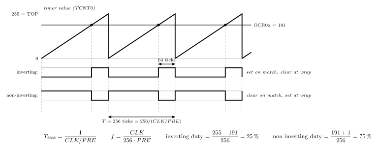
Figure 11: Fast PWM with a fixed top of 255 (mode 3, WGM[2:0] = 011) on an 8-bit timer. The count climbs one step per prescaled clock tick from 0 to 255 and wraps, so every period is exactly 256 ticks and the frequency is \(CLK/(256 \cdot PRE)\) regardless of the compare value. The compare register draws a line across the ramp; the pin switches at the crossing and switches back at the wrap. In inverting mode the pin goes high at the match and low at the wrap, so it is high for \(255 - OCR\) ticks; with \(OCR = 191\) that is 64 ticks of 256, a 25,% duty cycle. Non-inverting mode is the same crossing with the polarity swapped: high for \(OCR + 1\) ticks, 75,% here. The two outputs always add up to a full period, so the two modes are one signal and its complement.
Reading the formulas. The prescaler sets the tick, the fixed 256-count sweep sets the period, and only the compare value moves the edge. So in mode 3 frequency and duty cycle are set by different registers and do not interact, which is convenient. The cost is that the frequency can only take the eight values \(CLK/(256 \cdot PRE)\) allows: at 8 MHz, from 31.25 kHz down to 30.5 Hz. If none of those is right, mode 7.
Fast PWM mode — WGM[2:0] = 111 (0x7)
The count now climbs from 0 to OCR0A, which is 1 + OCR0A ticks. TOP is OCR0A, not 255. Take OCR0A = 127 and OCR0B = 95, a gap of 32 counts.
\[T_{tick} = \frac{1}{CLK / PRE} \qquad\qquad T = \frac{1 + OCR0A}{CLK / PRE} \qquad\qquad f = \frac{CLK}{(1 + OCR0A) \cdot PRE}\]
\[\text{duty cycle} = \frac{32}{128} \cdot 100\% = \mathbf{25\%}\]
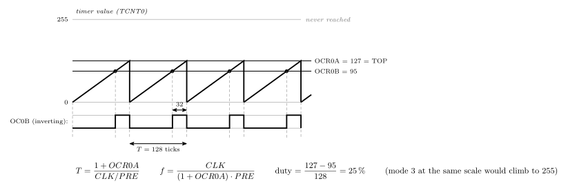
Figure 12: Fast PWM with OCR0A as the top (mode 7, WGM[2:0] = 111). The count now wraps when it reaches OCR0A instead of 255, so the period is \(OCR0A + 1\) ticks and can be chosen freely instead of being fixed at 256; the frequency becomes \(CLK/((OCR0A+1)\cdot PRE)\). The pulse is generated on the other compare unit: OCR0B draws the line across the shorter ramp and the OC0B pin switches at that crossing. With \(OCR0A = 127\) and \(OCR0B = 95\) the period is 128 ticks and the inverting output is high for \(127 - 95 = 32\) of them, again 25,%. Compare unit A is spent on setting the period, so mode 7 buys frequency control by giving up one of the two PWM outputs; OC0A can at most toggle at each wrap.
The trade. Mode 3 gives two PWM outputs at a fixed frequency; mode 7 gives one PWM output at a chosen frequency. The general formula behind both, \(f = CLK / (PRE \cdot (TOP + 1))\), is the master formula Lab 12 works from, with \(TOP\) = 255 or \(OCR0A\) as the mode dictates (avr-timers-and-counters).
Phase correct PWM
- The centres of the pulses remain at the same point in the period. At 25 %, 50 % and 75 % the centres line up.
- It is better for motor speed control.
- It is implemented by having the timer count up and then down.
- It is not used in this course, which uses fast PWM mode only.
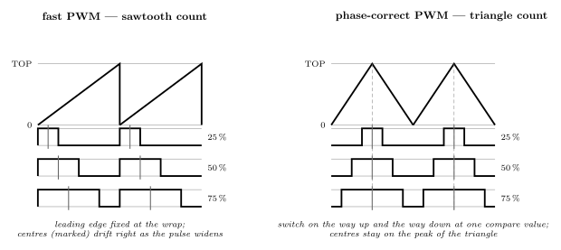
Figure 13: Fast PWM against phase-correct PWM, for the same three duty cycles. In fast PWM the count is a sawtooth and every pulse starts at the wrap, so its leading edge is fixed and widening the pulse moves only the trailing edge: the pulse’s centre drifts as the duty cycle changes. In phase-correct PWM the count climbs and then descends, and the pin switches on the way up and back on the way down at the same compare value, so the pulse is symmetric about the peak of the triangle: its centre stays put and both edges move outward together. For a motor that is smoother, because the current pulse’s timing relative to the period does not shift as the speed is changed; the price is that the triangle takes twice as long, halving the frequency. This course uses fast PWM only.
Counting up and then down is the whole mechanism: the compare line is crossed twice per triangle, once rising and once falling, and the two crossings are equidistant from the peak. Nothing in the labs or the assignment needs it; fast PWM is the mode the course uses, and it is the one Lab 12’s master formula and the WGM tables describe.
See also
- pulse-width-modulation — duty cycle, average value, the two fast PWM modes and their formulas, inverting versus non-inverting
- avr-timers-and-counters — the three timers, their registers, prescaler, modes and pins
- 2026-09-14-flow-of-control — Lecture 15, where the timers were introduced
- week8-lab-avr-timers — Lab 12:
TCCR1A/B/C,WGM,CSandCOMbit by bit, and the master formula - week9-lab-avr-pwm — Lab 13: PWM on the board
- avr-io-ports · avr-architecture · timing-diagrams · [counters]
Lab 11 — AVR C Programming
Learning Lab 11, the first lab in C. The seven-segment program from 2026-09-10-more-c-programming-on-the-avr is typed in, wired up and extended to hex digits and to a two-input adder. It also covers the bit-shift and bit-mask idioms that every AVR C program from here on is written in. See seven-segment-display for the display and its lookup table, bit-masking for the four masking operations, and c-operators for <<, |, & and ^.
What this lab covers
- Microchip Studio C programming
- AVR C programming exercises
Ed Lessons
The Ed discussion board also provides Ed Lessons, designed to instruct you in the basics of C. The content should be no more complex than CSSE1001 content. C programming for the AVR starts in week eight, with this lab.
The lessons are released in stages:
| Date | Lesson |
|---|---|
| 14 Aug | Basics |
| 28 Aug | Next Steps #1 |
| 11 Sep | Next Steps #2 |
| 25 Sep | Extension Tasks |
| 16 Oct | Floating Point Workshop |
The first three were out before this lab.
Worked: (23>>2)<<3
What is printed by this line of code:
printf("%d", (23>>2)<<3);
40.
Work it in binary, because the two shifts do not cancel:
| Step | Binary | Decimal |
|---|---|---|
23 |
1 0 1 1 1 |
23 |
23 >> 2 |
1 0 1 |
5 — the two low bits 11 fall off the end |
5 << 3 |
1 0 1 0 0 0 |
40 |
>> 2 is division by 4 with the remainder thrown away — \(\lfloor 23/4 \rfloor = 5\) — and << 3 is multiplication by 8, so the result is \(8 \cdot 5 = 40\), not \(23 \cdot 2 = 46\). The bits shifted out on the right are gone; shifting back left fills with zeros (c-operators). It is the same loss of information a lsr has in assembly, where the dropped bit lands in C and the next lsl shifts in a 0 (avr-instructions).
Bit shifts and AVR code
It is common to use bit-shifts to indicate which bits are being operated on.
Example: set bit 5 of port B to be an output and other bits to be inputs.
| Assembly language | C equivalent |
|---|---|
ldi r16, (1<<5) out DDRB, r16 |
DDRB = (1<<5); |
1<<5 makes it clear bit 5 is being set. Both are the constant 0b00100000 = 0x20; the assembler evaluates (1<<5) at assembly time exactly as the C compiler does, so neither line costs anything at run time. The point is legibility: 0x20 has to be decoded, 1<<5 says bit 5 in the source. The AVR header files name every register bit this way, which is why (1<<CS11) turns up in week8-lab-avr-timers.
Setting bits and keeping the rest
Example: set bits 3 and 4 of port B to be outputs whilst keeping the direction of the other bits the same.
Assembly language:
    in   r16, DDRB
    ori  r16, (1<<4)|(1<<3)
    out  DDRB, r16
C equivalent:
DDRB |= (1<<4)|(1<<3);This is shorthand for DDRB = DDRB | ((1<<4)|(1<<3)); (c-operators). Read the three assembly lines against it: in is the read of DDRB on the right-hand side, ori is the |, out is the assignment back. A read-modify-write is three instructions in assembly and one operator in C, and it is the difference between this example and the previous one: DDRB = (1<<5) replaces the register, forcing the other seven bits to 0, whereas |= adds the two bits to whatever was there. The mask (1<<4)|(1<<3) is 0b00011000 = 0x18.
Bit masking operations — more than just bitwise ANDs
The four operations of bit-masking, now in C:
| Operator | Does | Example |
|---|---|---|
Bitwise AND & |
Clear particular bits (e.g. zero out high 4 bits) | var = PINB & 0x0F; |
| Test particular bits (e.g. is bit 1 set?) | if(PINB & 0x02) … |
|
Bitwise OR \| |
Set particular bits (e.g. set sign bit to 1) | PORTC = PINB \| 0x80; |
Bitwise XOR ^ |
Invert particular bits (e.g. invert low 4 bits) | PORTC = PINB ^ 0x0F; |
The rule for building a mask is the same in every row: put a 1 on the bits the operation should touch — keep, for AND; set, for OR; flip, for XOR — and a 0 everywhere else. 0x0F appears twice with two meanings: with & it keeps the low nibble, with ^ it inverts it.
The test row is the one that is new. PINB & 0x02 is 0x02 if bit 1 is set and 0x00 if not, and since C treats any non-zero value as true (c-control-flow) that expression can sit directly inside an if. It does not need to be compared with 1 — and must not be, because it never is 1.
Seven segment display
- LEDs arranged in a pattern
- Eight segments if DP (decimal point) is included
- One byte drives it, e.g.
0001 1110₂ with the “A” segment as LSB and the “DP” segment as MSB
The segments are lettered A across the top, B upper right, C lower right, D bottom, E lower left, F upper left, G across the middle, and DP the dot — the same lettering as seven-segment-display, just in capitals. With A at bit 0 and DP at bit 7 the byte reads, MSB first, DP G F E D C B A, so 0001 1110 lights E, D, C and B: the right-hand side, the bottom and the lower left — a shape like a J.
Worked: what 0011 1110₂ then 1111 0100₂ spell out (“A” = LSB)
“Uh.”
| Byte | DP G F E D C B A |
Lit | Shows |
|---|---|---|---|
0011 1110 |
0 0 1 1 1 1 1 0 |
F E D C B | U |
1111 0100 |
1 1 1 1 0 1 0 0 |
DP G F E C | h with the dot: h. |
In the second byte, F, E and G make the left-hand upright and the middle bar; C adds the lower right; no A, so the top is open and the shape is a lowercase h rather than an H. Bit 7 lights the decimal point after it. Task 2 turns this reading-off into writing the six hex letters.
Tasks
Task 1 — Seven Segment Display
- Create an AVR C project and type in and build the seven-segment display (SSD) example from lecture 14. The code is also on Blackboard.
- Connect up AVR pins to the IO board pins:
- Connect IO board SSD inputs (A to G and DP) to port A (you can use 2 × 4-way cables and headers for this. SSD pin A should be connected to the least significant bit of port A.)
- Connect IO board pin CC (SSD digit select input) to button B0
- Connect IO board switches 0 to 3 to the lower four pins of port C
- Download your program to the board and test it — check that the number you enter on switches 0 to 3 shows up as a digit on the seven-segment display. Press and release button B0 and check that the number shows up on the other SSD digit.
Task 2 — Adding Hex Patterns
- Modify the task 1 code so that your program can also output values 10 to 15 as hex digits as shown in the following patterns: A b C d E F.
- Build, download and test your program.
Task 3 — Addition Results on SSD
- Write a program that repeatedly reads the lower 4 bits of port A and the lower 4 bits of port B and adds these two values together and displays (on the SSD, using a port of your choice) the hexadecimal value of the lower 4 bits of the result.
- Wire up the IO board and AVR 324 Dev board as required.
- Build, download and test your program.
Task 4 — Bitmasking
- Download
lab11-task4.cfrom Blackboard - Read through the comments at the start of the code
- Run the code as-is and observe the issues
- Fix the code by bitmasking where required
- Interrupts will be explained in Lec 17 then Lab 14
Working — Task 1
The project. In Microchip Studio a C project is a GCC C Executable Project for the ATmega324A, the same device selection as the assembly projects of week5-lab-avr-assembly-one; the file it gives you is main.c. The program is the one from Lecture 14, unchanged:
#include <avr/io.h>

/* Seven segment display values */
uint8_t seven_seg[10] = { 63,6,91,79,102,109,125,7,127,111};

int main(void) {
  uint8_t digit;

  /* Set port A pins to be outputs, port C pins to be inputs */
  DDRA = 0xFF;
  DDRC = 0;    /* This is the default, could omit. */
  while(1) {
    /* Read in a digit from lower half of port C pins */
    /* We read the whole byte and mask out upper bits */
    digit = PINC & 0x0F;
    /* Write out seven segment display value to port A */
    if(digit < 10) {
      PORTA = seven_seg[digit];
    } else {
      PORTA = 0;
    }
  }
}
Every line is explained in 2026-09-10-more-c-programming-on-the-avr. The new part is the wiring, and the wiring has one rule that the code silently depends on: SSD pin A goes to PA0. The lookup table was built with segment a at bit 0 and dp at bit 7, so the cable must carry that order across — A on PA0 up through G on PA6 and DP on PA7. Get the two 4-way cables swapped and every digit comes out scrambled.
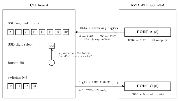
Figure 14: The three connections Task 1 asks for, and what each one means for the program. Port A carries the eight segment lines in the same order as the bits of the lookup table, so PORTA = seven_seg[digit] lights a digit with no further translation. The low four bits of port C read the switches, and & 0x0F discards the four unconnected pins above them. The CC line is not driven by the AVR at all: it is jumpered to button B0 on the board, so the button alone decides which of the two digits shows the pattern — which is why pressing it moves the number across without the program doing anything.
Testing (c). Set a number on switches 0–3 and the matching digit should appear. The interesting test is the button: CC is wired to B0, not to the AVR, so pressing it changes the common-cathode select in hardware and the same pattern appears on the other digit — the program has not changed, only which digit’s cathode is connected (seven-segment-display). Switch values 10–15 blank the display, which is the else branch doing its job; Task 2 is about making them show something instead.
Working — Task 2
Six more entries and the display can show every value four bits can hold. The patterns are A b C d E F, and the case is not cosmetic. An uppercase B on seven segments is indistinguishable from 8, and an uppercase D from 0, so those two are drawn lowercase; the other four have no such clash and stay capitals.
| Digit | Segments lit | dp g f e d c b a |
Decimal |
|---|---|---|---|
| A | a b c e f g | 0111 0111 |
119 |
| b | c d e f g | 0111 1100 |
124 |
| C | a d e f | 0011 1001 |
57 |
| d | b c d e g | 0101 1110 |
94 |
| E | a d e f g | 0111 1001 |
121 |
| F | a e f g | 0111 0001 |
113 |
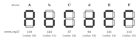
Figure 15: The six hex letters as seven-segment patterns, with the byte that produces each one in decimal underneath, ready to append to the lookup table. Heavy segments are lit; the bit order is dp g f e d c b a with a at bit 0, as for the ten decimal digits. The letters b and d are the lowercase forms because their capitals would be indistinguishable from 8 and 0 on this display: b is 8 without segments a and b, d is 0 with the top-left corner (a, f) removed and the middle bar g added.
The change to the program is two lines: the table grows to sixteen entries, and the guard is no longer needed because four input bits cannot index past it.
#include <avr/io.h>

/* Seven segment display values: 0-9 then A b C d E F */
uint8_t seven_seg[16] = { 63,6,91,79,102,109,125,7,127,111,
                          119,124,57,94,121,113 };

int main(void) {
  uint8_t digit;

  DDRA = 0xFF;                 /* segments out on port A */
  DDRC = 0;                    /* switches in on port C */
  while(1) {
    digit = PINC & 0x0F;       /* 0 to 15 - every value is now a valid index */
    PORTA = seven_seg[digit];
  }
}
Dropping the if is safe only because of the mask on the line above it: PINC & 0x0F is at most 15 and seven_seg[15] exists. Leaving the guard in as if(digit < 16) costs nothing and documents the assumption; taking the mask out would be the bug (c-pointers-and-arrays — C will not stop an index at 16).
Working — Task 3
Two 4-bit inputs, one 4-bit output. The task fixes the inputs — low nibble of port A, low nibble of port B — and leaves the output port to you; port C is used here, the port Task 1 used for input, with the SSD moved across to it. Port D would do equally well.
#include <avr/io.h>

/* 0-9 then A b C d E F, as in Task 2 */
uint8_t seven_seg[16] = { 63,6,91,79,102,109,125,7,127,111,
                          119,124,57,94,121,113 };

int main(void) {
  uint8_t a, b, sum;

  DDRA = 0;                    /* switches 0-3 on PA0-PA3 */
  DDRB = 0;                    /* switches 4-7 on PB0-PB3 */
  DDRC = 0xFF;                 /* SSD segments on port C  */
  while(1) {
    a = PINA & 0x0F;           /* extract the low nibble of each port */
    b = PINB & 0x0F;
    sum = (a + b) & 0x0F;      /* add, then keep the low 4 bits of the result */
    PORTC = seven_seg[sum];    /* show it as a hex digit */
  }
}
Three things the wording of the task decides:
- Both masks are needed, not just one. The upper four pins of each port are unconnected and read as unpredictable values, so without the
& 0x0Fthe sum would include junk (week6-lab-avr-io-ports hit the same thing withandi). - The result is masked too. The largest sum is \(15 + 15 = 30\), which fits comfortably in a
uint8_t, so nothing overflows in C; but the task asks for the lower 4 bits of the result, so bit 4 — the carry out of the nibble — is discarded. $9 + 9 = 18 = $0x12shows as 2, and $8 + 8 = 16 = $0x10shows as 0. That is the answer, not a bug: it is the four-bit adder of 2026-08-04-binary-arithmetic with its carry-out unconnected. - The hex table from Task 2 is what makes it display. Sums of 10 to 15 are common (7 + 5, say), and they must show as hex letters, which is why the task follows Task 2 rather than preceding it.
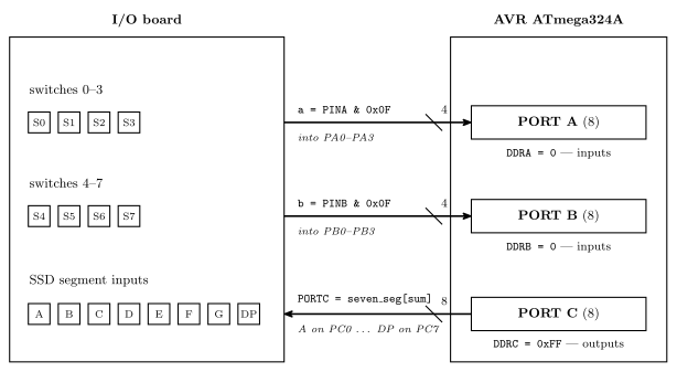
Figure 16: The Task 3 wiring. Two nibbles of switches come in on the low halves of ports A and B, the SSD segment lines go out on port C, and the direction registers follow: 0 for the two input ports, 0xFF for the output port. The upper four pins of ports A and B are left unconnected, which is what makes the & 0x0F on each read necessary rather than decorative. CC can be left tied to a button as in Task 1; the program only ever drives one digit.
Testing. With all eight switches down the display shows 0; raise switch 0 alone and it shows 1, switch 4 alone and it also shows 1 (that is the other operand); switches 0 and 4 together show 2. Setting both nibbles to 1111 shows E: $15 + 15 = 30 = $ 0x1E, low nibble E.
Working — Task 4
lab11-task4.c is a Blackboard download. The exercise is a program that runs but misbehaves, where every fault is a whole-port write or read that should have been a masked one. The toolkit for fixing it is the bit-masking table above, applied at the points where a program touches only some of a port’s pins:
| Symptom | Likely line | Fix |
|---|---|---|
| Setting one pin’s direction disturbs the others | DDRx = (1<<n); |
DDRx \|= (1<<n); |
| Writing one output changes neighbouring outputs | PORTx = value; |
PORTx = (PORTx & ~mask) \| (value & mask); — or \|= / &= for a single bit |
| An input test is never true | if(PINx & (1<<n) == 1) |
if(PINx & (1<<n)) — the result is 1<<n, not 1 |
| Unconnected pins leak into a value | var = PINx; |
var = PINx & 0x0F; |
The third row is the test case from the bit-masking table: PINB & 0x02 is either 0x02 or 0, and comparing it to 1 is always false.
Interrupts are explained in Lecture 17, then Lab 14. The downloaded file presumably contains an interrupt handler, which is to be left alone for now; only the masking is to be fixed. Lecture 17 is 2026-09-21-interrupts, and what an ISR(...) function is and how it gets called is in avr-interrupts.
See also
- seven-segment-display — segment lettering, the ten digit codes, and
CC - bit-masking — clear, test, set and invert, and why the masks are what they are
- c-operators —
<<,>>,&,|,^, and the|=shorthand - c-control-flow — why
if(PINB & 0x02)works without a comparison - avr-io-ports · io-board · c-preprocessor-and-avr-headers
- 2026-09-10-more-c-programming-on-the-avr — Lecture 14, where the Task 1 program comes from
- week6-lab-avr-io-ports — Lab 10, the same wiring exercises in assembly
- week8-lab-avr-timers — Lab 12, where
(1<<CS11)and friends configure a timer - avr-interrupts — the
ISR()handlers the lab code contains
Lab 12 — AVR Timers
Learning Lab 12, where a timer/counter is configured for the first time: which I/O registers are involved, how the control bits are laid out, the one formula that turns a wanted frequency into register values, and two programs — a hardware-toggled LED and a two-digit multiplexed display driven by a pulse counter. The timers themselves are in avr-timers-and-counters; the lectures this lab builds on are 2026-09-14-flow-of-control (Lecture 15, the introduction) and 2026-09-17-pulse-width-modulation (Lecture 16).
Outline
- AVR timers
- the I/O registers involved
- how to set up a timer
- Exercises
ATmega324A — timer/counter summary
The ATmega324A has three timer/counters, separate hardware from the CPU. The datasheet block diagram names them 8bit T/C 0, 16bit T/C 1 and 8bit T/C 2. Between them they have six output-compare pins on the 40-pin package: OC0A/OC0B on PB3/PB4, OC1A/OC1B on PD5/PD4, OC2A/OC2B on PD7/PD6 (avr-architecture).
| Timer/Counter 0 | Timer/Counter 1 | Timer/Counter 2 | |
|---|---|---|---|
| Pins | PB3 (OC0A) & PB4 (OC0B) | PD5 (OC1A) & PD4 (OC1B) | PD7 (OC2A) & PD6 (OC2B) |
| Width | 8-bit timer/counter | 16-bit timer/counter | 8-bit timer/counter |
| PWM | Supports PWM | Supports PWM | Supports PWM |
| Modes of operation | Normal, CTC, Fast-PWM and phase correct PWM | Normal, CTC, Fast-PWM, PC-PWM and PFC-PWM | Normal, CTC, Fast-PWM and phase correct PWM |
| Clock prescalar | No clock, F, F/8, F/64, F/256, F/1024 | No clock, F, F/8, F/64, F/256, F/1024 | No clock, F, F/8, F/32, F/64, F/128, F/256, F/1024 |
| I/O registers | TCNT0; TCCR0A, TCCR0B; OCR0A, OCR0B; TIMSK0, TIFR0 | TCNT1H, TCNT1L; TCCR1A, TCCR1B, TCCR1C; OCR1AH, OCR1AL, OCR1BH, OCR1BL; TIMSK1, TIFR1 | TCNT2; TCCR2A, TCCR2B; OCR2A, OCR2B; TIMSK2, TIFR2 |
Read the three columns as one design in three sizes. Every unit has the same four kinds of register — a count (TCNTn), control (TCCRnA/B), output compare (OCRnA/B) and interrupt (TIMSKn, TIFRn) — and two output-compare pins. Timer 1 is the odd one out only in width: 16 bits means every data register comes as a high/low pair and there is a third control register. Timer 2 has two extra prescaler taps. The lab works timer 1 in Task 1 and timer 0 in Task 2.
Timer/counter clock sources
There are 3 timer/counters:
- 0: 8 bit (0 to 255)
- 1: 16 bit (0 to 65535)
- Clock sources: STOPPED, CLK, CLK/8, CLK/64, CLK/256, CLK/1024, external pin rising edge, external pin falling edge. CLK = system clock.
- 2: 8 bit (0 to 255)
- Clock sources: STOPPED, CLK, CLK/8, CLK/32, CLK/64, CLK/128, CLK/256, CLK/1024. CLK = system clock or external oscillator.
“External pin” for timers 0 and 1 is the T0/T1 pin (the clock-selection section below says which pin), and it is what makes those two counters as well as timers: fed from a button instead of the system clock, TCNT0 counts presses. Timer 2 has no external-pin option; its alternative is a crystal on TOSC1/TOSC2.
Timer/counter registers — TCNT, count values
| Register | Memory address | I/O register |
|---|---|---|
| TCNT0 | 0x46 | 0x26 |
| TCNT1 (16 bits) — TCNT1L | 0x84 | — |
| TCNT1H | 0x85 | — |
| TCNT2 | 0xB2 | — |
Only TCNT0 has an I/O-register number, and so only TCNT0 is reachable with in/out (avr-io-ports — I/O numbers stop at 0x3F). The others sit in the extended I/O region and need lds/sts in assembly; in C the distinction disappears, because the header defines every one of them as a memory address (c-preprocessor-and-avr-headers) and TCNT1 = 0; is legal whichever region it lives in.
Output compare registers
Each timer/counter has output compare registers (these are I/O registers). They are for matching timer/counter values. Actions can be taken when the value is reached, e.g.
- set the output-compare match bit in a register
- clear the timer (reset to 0)
- toggle / set / clear an external pin
| Timer | Registers |
|---|---|
| Timer 0 (8 bit) | OCR0A, OCR0B |
| Timer 1 (16 bit) | OCR1AH, OCR1AL (in C, access as 16-bit “variable” OCR1A); OCR1BH, OCR1BL (in C: OCR1B) |
| Timer 2 (8 bit) | OCR2A, OCR2B |
The three actions are three separate things the hardware can do at the instant TCNTn equals OCRnA (or OCRnB), and they are enabled independently: the flag bit is always set; clearing the timer happens only in CTC mode (the WGM bits); the pin action is chosen by the COM bits. Task 1 uses all three at once — CTC to set the period, the pin toggle to make the LED blink, and nothing reads the flag; Task 2 uses the flag alone as a 1 ms tick.
Accessing 16-bit I/O registers
Example: set output compare register 1B (16 bits) to 4321.
In assembly language:
    ldi  r16, high(4321)
    sts  OCR1BH, r16
    ldi  r16, low(4321)
    sts  OCR1BL, r16
The processor requires the high byte to be written first.
In C:
OCR1B = 4321;The order is not a style rule. The 16-bit timer registers share one hidden temporary byte: a write to the high byte goes into the temporary register, and a write to the low byte transfers both bytes into the real register in one go, so that the hardware never sees a half-updated value. High first, low second, is what makes that work — and the compiler knows it, which is why the C line is one assignment. sts rather than out because OCR1BH/OCR1BL are beyond the 64 I/O registers (avr-io-ports). Reading goes the other way, low byte first, for the same reason.
Setting up a 16-bit timer
A 16-bit timer has 3 control registers. For timer/counter 1 (n = 1) the “n” in each bit name is replaced by 1, e.g. COM1A1, COM1A0, COM1B1, COM1B0.
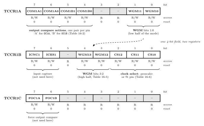
Figure 17: The three control registers of timer/counter 1 in the datasheet’s three-row form: bit numbers above, bit names in the boxes, access and reset value below. Grey boxes are reserved and read as 0. The bits that matter group into four fields, and one of them — the waveform generation mode — is split across two registers, WGM11:10 at the bottom of TCCR1A and WGM13:12 in the middle of TCCR1B, so a four-bit mode number has to be written in two halves. Everything a normal program sets lives in TCCR1A and TCCR1B; TCCR1C is left at 0.
The pattern to notice is that the register letter and the pin letter are different things. COM1A1 and COM1A0 are the two bits for pin OC1A; COM1B1 and COM1B0 are for OC1B; and both pairs live in TCCR1A.
The different “A”s
Names with an “A” in them:
| COMnA | OCnA | TCCRnA |
| OCRnA | OCIEnA | PINA |
| PORTA | ||
| DDRA |
These fall into three groups. The items in each group are related, but each group is independent of the others: the “A”s are different “A”s.
- Channel A of a timer —
COMnA(its output-compare action bits),OCRnA(its compare register),OCnA(its pin),OCIEnA(its interrupt enable). These four do go together: one compare channel, one letter. - Control register A —
TCCRnAis simply the first of the timer’s control registers. It holds channel B’s COM bits as well as channel A’s, so the A here is not the channel. - Port A —
PINA,PORTA,DDRAare a GPIO port and have nothing to do with timers at all.
There are 2 hard problems in computer science: cache invalidation, naming things, and off-by-1 errors. The off-by-one matters here: it is the + 1 in the master formula below, and Task 0 turns on it.
WGM — waveform generation modes
WGM11, WGM10 are bits 1 and 0 of TCCR1A; WGM13, WGM12 are bits 4 and 3 of TCCR1B (Figure 17).
Table 16-5 on page 138 of the datasheet describes the modes. Two are of interest:
- 0:
0000— normal. The count goes 0 → 1 → … → 65535 → 0 → … - 4:
0100— CTC, Clear Timer on Compare match. The counter resets to 0 when it reaches the value in theOCR1Aregister.
Mode 4 is the one that makes a timer programmable. In normal mode the period is fixed by the width — 65 536 counts, whatever the prescaler — and the only way to get a different period is to reload TCNT1 by hand. In CTC the period is OCR1A + 1 counts, chosen by the program, and the reset is done by the hardware. The fast PWM modes of Lecture 16 are the other members of this table (pulse-width-modulation).
The master formula
\[f_{\text{event}} = \frac{f_{\text{clk\_I/O}}}{N \cdot (\text{TOP} + 1)}\]
- \(f_{\text{clk\_I/O}}\) is the clock frequency of the device — 8 MHz for the ATmega324A.
- \(N\) is the prescaler.
- TOP is the maximum value that the timer will reach. This can be some fixed constant, or a value in an output compare register.
- \(f_{\text{event}}\) is the frequency of the event in question.
What event means, case by case:
- For hardware pin toggling, \(f_{\text{event}}\) is the frequency that the pin is toggled. The waveform consists of one falling edge and one rising edge. The frequency of that waveform is thus half of \(f_{\text{event}}\).
- For PWM (more on that in a later lab), \(f_{\text{event}}\) is the frequency of falling edges in non-inverting mode, and the frequency of rising edges in inverting mode.
- For interrupts (more on that in a later lab), \(f_{\text{event}}\) is the frequency that the interrupt runs.
Why the formula has the shape it does: the counter ticks at \(f_{\text{clk}} / N\) and each period is \(\text{TOP} + 1\) ticks long — from 0 up to TOP inclusive — so a period lasts \(N (\text{TOP}+1) / f_{\text{clk}}\) seconds and the event happens once per period. The \(+1\) is the off-by-one: TOP is the last value counted, not the number of values.
Worked: what is the frequency of this wave?
A sine wave is plotted on an axis marked 0 at the left and 1 at the right, and it completes three full cycles between the two marks. What is its frequency?
3 Hz. Three cycles per unit of time is 3 Hz, taking the unlabelled 0 and 1 as seconds. 6 Hz is wrong: it counts the half-cycles — each hump — which is the pin-toggling trap again: six edges per second is three cycles per second. 8 MHz is the AVR’s clock, not this wave.
Clock selection
CS12, CS11, CS10 are bits 2–0 of TCCR1B. From Table 16-6 on page 139 of the datasheet (here n = 1):
| CSn2 | CSn1 | CSn0 | Description |
|---|---|---|---|
| 0 | 0 | 0 | No clock source (Timer/Counter stopped) |
| 0 | 0 | 1 | clk\(_{\text{I/O}}\)/1 (No prescaling) |
| 0 | 1 | 0 | clk\(_{\text{I/O}}\)/8 (From prescaler) |
| 0 | 1 | 1 | clk\(_{\text{I/O}}\)/64 (From prescaler) |
| 1 | 0 | 0 | clk\(_{\text{I/O}}\)/256 (From prescaler) |
| 1 | 0 | 1 | clk\(_{\text{I/O}}\)/1024 (From prescaler) |
| 1 | 1 | 0 | External clock source on Tn pin. Clock on falling edge |
| 1 | 1 | 1 | External clock source on Tn pin. Clock on rising edge |
The T1 pin is port B, pin 1 (PB1, package pin 2, PCINT9/CLKO/T1; see p11 of the datasheet). The table is the clock-selection mux from Lecture 15: three bits pick one of eight inputs, and 000 is the stopped input, which is why writing zero to the CS bits is how a timer is switched off — and why a timer whose CS bits have not been set does nothing at all.
Clock selection — code example
Row 0 1 1 of the table — clk\(_{\text{I/O}}\)/64 (from prescaler) — is:
TCCR1B = (1<<CS11) | (1<<CS10);Bit labels can be used in code expressions. CS11 and CS10 are defined in the header as the bit numbers 1 and 0 (c-preprocessor-and-avr-headers), so (1<<CS11)|(1<<CS10) is 0b011 = 0x03, and the assignment also writes 0 to every other bit of TCCR1B — normal mode, no input capture. That is fine for this line but it is the reason Task 1 has to put its WGM bit in the same expression: a second TCCR1B = (1<<WGM12); would wipe the clock select out again (bit-masking).
Output compare actions — can toggle/clear/set pin
COM1A1, COM1A0, COM1B1, COM1B0 are bits 7–4 of TCCR1A. From Table 16-2 on page 136 of the datasheet (n = 1):
| COMnA1/COMnB1 | COMnA0/COMnB0 | Description |
|---|---|---|
| 0 | 0 | Normal port operation, OCnA/OCnB disconnected |
| 0 | 1 | Toggle OCnA/OCnB on Compare Match |
| 1 | 0 | Clear OCnA/OCnB on Compare Match (Set output to low level) |
| 1 | 1 | Set OCnA/OCnB on Compare Match (Set output to high level) |
The OC1A pin, for example, is PD5, package pin 19 (see p11 of the datasheet). Two things follow. Any non-zero COM value takes the pin away from the port — PORTD bit 5 no longer drives it, the timer does — so the pin changes from GPIO to timer/counter operation. And the pin still has to be made an output with DDRD, because the timer only decides the value, not the direction.
Tasks
Task 0
To toggle an output compare pin 8 times per second (4 Hz period) with timer/counter 1, what
- clock prescale
- output compare
values do we need?
Task 1 — Output Compare Based Timer
- Consider
lab12-1.c(on Blackboard). - The code is to toggle the OC1A pin (what pin is this?) 8 times per second (i.e. 4 Hz period).
- This pin is connected to an LED (e.g. LD0).
- Fill in the blanks to make the code work.
- Set up the hardware to do the work; software does nothing after that.
- Build and test your code on the AVR board.
- Look at the generated list (
lss) file for the assembly language equivalent.
Working — Task 0
“Toggle 8 times per second” is the event rate: \(f_{\text{event}} = 8\ \text{Hz}\). Each toggle is one edge, so the LED waveform has 4 rising edges a second — the task’s “4 Hz period” — and the pin-toggling rule (waveform frequency is half of \(f_{\text{event}}\)) is what reconciles the two numbers.
Put \(f_{\text{clk}} = 8\,\text{MHz}\) and \(f_{\text{event}} = 8\,\text{Hz}\) into the master formula and solve for the product:
\[N \cdot (\text{TOP} + 1) = \frac{8\,000\,000}{8} = 1\,000\,000\]
Then try each prescaler timer 1 offers:
| \(N\) | \(\text{TOP} + 1 = 10^6 / N\) | TOP | Usable? |
|---|---|---|---|
| 1 | 1 000 000 | 999 999 | no — timer 1 stops at 65 535 |
| 8 | 125 000 | 124 999 | no — too big for 16 bits |
| 64 | 15 625 | 15 624 | yes — exact |
| 256 | 3 906.25 | — | no — not a whole number |
| 1024 | 976.5625 | — | no — not a whole number |
So prescaler 64 (CS12:0 = 011) and OCR1A = 15624 in CTC mode, where TOP is OCR1A. It is the only combination that is both exact and fits, which is typical: the prescaler is chosen to bring TOP under 65 536, and then TOP is whatever the division leaves. The 256 and 1024 rows could be used at the cost of a fractional error (OCR1A = 3905 gives 8.00195 Hz), but the task wants the exact one.
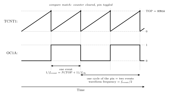
Figure 18: Clear-timer-on-compare mode with the output-compare pin set to toggle. The count climbs from 0 at the prescaled clock rate, reaches OCR1A (the TOP value), and is cleared to 0 by the hardware on the same tick that OC1A flips. One compare match is one event, so the events come at \(f_{\text{clk}} / (N(\text{TOP}+1))\) — but the pin only completes a full high-then-low cycle every two events, which is why the waveform on the LED runs at half the event frequency. With \(N = 64\) and \(\text{TOP} = 15624\) the matches are 125 ms apart and the LED cycle is 250 ms.
Working — Task 1
lab12-1.c is a Blackboard download with blanks to fill in. The task fixes what the blanks must produce, and the whole configuration is four register writes plus one direction bit, so the program is given in full here and can be matched against the download line by line.
What pin is OC1A? PD5 — package pin 19, PCINT29/OC1A. It has to be wired to an LED (LD0 on the IO board) and made an output.
#include <avr/io.h>

int main(void) {
  /* OC1A is PD5 - the timer decides its value, but it must be an output */
  DDRD |= (1<<5);

  /* Start counting from 0, and set the period: TOP = 15624 with N = 64
     gives 8 MHz / (64 * 15625) = 8 compare matches per second */
  TCNT1 = 0;
  OCR1A = 15624;

  /* Toggle OC1A on compare match: COM1A1:0 = 01.  WGM11:10 = 00. */
  TCCR1A = (1<<COM1A0);

  /* CTC mode: WGM13:12 = 01 (mode 4 = 0100).  Prescaler 64: CS12:0 = 011.
     This write starts the timer, so it comes last. */
  TCCR1B = (1<<WGM12) | (1<<CS11) | (1<<CS10);

  while(1) {
    /* Nothing.  The hardware toggles the pin; the CPU is idle. */
  }
}
Points where a blank is easy to get wrong:
- Mode 4 is
0100, split across the registers:WGM12is the only 1, and it is inTCCR1B(Figure 17).WGM11/WGM10inTCCR1Astay 0. - Toggle is
COM1A0alone (01), inTCCR1A. SettingCOM1A1instead gives clear on match (10), and the pin goes low once and stays there. - The clock-select bits and the WGM bit go in one assignment. Two separate
TCCR1B = …lines would each erase the other’s bits;|=on both would also work. OCR1A = 15624, not 15625. TOP is the last value counted; the period is TOP + 1 ticks.- Order:
OCR1Abefore the clock is started, so the first period is the right length;TCNT1 = 0is what reset leaves anyway, but writing it makes the intent visible.
Software does nothing after that — the while(1) body is empty and the LED blinks regardless. That is the point of the exercise: the timer is separate hardware, and a program that has set it up can go on to do anything else, or nothing.
The .lss file is the compiler’s listing, C source interleaved with the assembly it became. The five register writes appear as ldi/out for DDRD and TCCR1A… and ldi/sts pairs for OCR1A and TCNT1, high byte then low byte, exactly as under Accessing 16-bit I/O registers above; the empty loop is a single rjmp to itself (avr-program-structure).
Working — Task 2
lab12-2.c is also a Blackboard download with blanks to fill in. The task statement is enough to write the program, so what follows is a complete version that meets it; the download will have the same registers in its blanks.
Which pin is T0? From the pinout, T0 is on PB0 — package pin 1, PCINT8/XCK0/T0. (T1 is PB1, as in the clock-selection section.) The push button goes there, and it must be an input.
Two timers do two jobs:
- Timer/counter 0 counts the presses. Clock select
111— external clock source on T0 pin, clock on rising edge — in normal mode. Every rising edge onPB0adds one toTCNT0, with no software involved; the program just readsTCNT0when it wants the count. - Timer/counter 1 provides the 1 ms tick. CTC mode with
OCR1Afrom the master formula: \(f_{\text{event}} = 1000\,\text{Hz}\), so \(N(\text{TOP}+1) = 8000\); \(N = 8\), \(\text{TOP} = 999\). Nothing is wired toOC1Athis time — the program polls the compare-match flag,OCF1AinTIFR1, which the hardware sets on every match. The flag is cleared by writing a 1 to it.
#include <avr/io.h>

/* Seven segment display values */
uint8_t seven_seg[10] = { 63,6,91,79,102,109,125,7,127,111 };

int main(void) {
  uint8_t count;
  uint8_t left = 0;             /* which digit is lit this millisecond */

  DDRA = 0xFF;                  /* segments on port A            */
  DDRD |= (1<<0);               /* CC on PD0                     */
  DDRB &= ~(1<<0);              /* T0 = PB0 is an input          */

  /* Timer/counter 0: normal mode, clocked by rising edges on T0 */
  TCNT0 = 0;
  TCCR0A = 0;
  TCCR0B = (1<<CS02) | (1<<CS01) | (1<<CS00);

  /* Timer/counter 1: CTC, compare match every 1 ms
     8 MHz / (8 * (999+1)) = 1000 Hz */
  TCNT1 = 0;
  OCR1A = 999;
  TCCR1A = 0;
  TCCR1B = (1<<WGM12) | (1<<CS11);

  while(1) {
    count = TCNT0 % 100;        /* two digits' worth of the running count */

    if(left) {
      PORTA = seven_seg[count / 10];     /* tens */
      PORTD |= (1<<0);                   /* CC = 1: left digit */
    } else {
      PORTA = seven_seg[count % 10];     /* ones */
      PORTD &= ~(1<<0);                  /* CC = 0: right digit */
    }

    /* Wait for the 1 ms compare match, then clear the flag */
    while((TIFR1 & (1<<OCF1A)) == 0) {
    }
    TIFR1 = (1<<OCF1A);

    left = !left;               /* other digit next time */
  }
}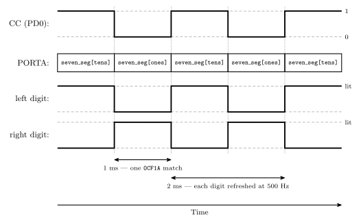
Figure 19: Display multiplexing on a 1 ms tick. The two digits share the eight segment lines, so only one can show its own pattern at a time; the program writes the tens pattern with CC high, waits 1 ms, writes the ones pattern with CC low, waits 1 ms, and repeats. Each digit is therefore lit half the time, at 500 Hz — far too fast for the eye to see it flicker, so both appear steady, at half brightness. Slow the tick to 250 ms and the same program visibly flips between the two digits, which is the task’s last step.
What each part is doing, and why:
TCCR0B = (1<<CS02)|(1<<CS01)|(1<<CS00)is row111of the clock-selection table, for timer 0. The button is the timer’s clock. A mechanical button bounces, so one press may register as several rising edges — the count can jump by two or three per press; that is the hardware being honest, not a bug in the code, and de-bouncing is a later problem.TCNT0 % 100— an 8-bit count runs 0–255, and two digits show 0–99, so the display shows the count modulo 100. Without this,count / 10reaches 25 and indexes past the end of the table (c-pointers-and-arrays).- The wait loop —
while((TIFR1 & (1<<OCF1A)) == 0)spins until the hardware sets the flag;TIFR1 = (1<<OCF1A)clears it by writing a 1 (a flag register clears the bits you write 1 to, the opposite of a port). The& (1<<OCF1A)is the test row of the bit-masking table from week8-lab-avr-c-programming. This is the software half of the compare match; Task 1 used the hardware half (the pin) and ignored the flag. - Segments before
CC. Each branch writes the pattern first and then selects the digit, so the newly selected digit never briefly shows the other digit’s pattern. left = !leftalternates;left ^= 1is the same thing spelled as an XOR mask.
Slowing it down — 4 times per second means a 250 ms tick: \(N(\text{TOP}+1) = 8\,000\,000 / 4 = 2\,000\,000\), and the only exact 16-bit fit is \(N = 64\), \(\text{TOP} = 31\,249\):
  OCR1A = 31249;
  TCCR1B = (1<<WGM12) | (1<<CS11) | (1<<CS10);   /* prescaler 64 */
Now the two digits are visibly taking turns, each on for a quarter of a second, and the multiplexing stops being an illusion.
See also
- avr-timers-and-counters — the three timer/counters, their registers, modes and the master formula
- pulse-width-modulation — the fast PWM modes, the other rows of the WGM table
- 2026-09-14-flow-of-control — Lecture 15: clock sources, prescaling and the clock-selection mux
- 2026-09-17-pulse-width-modulation — Lecture 16: the timer/counter summary and PWM
- seven-segment-display — the lookup table and
CC - bit-masking · c-operators · c-preprocessor-and-avr-headers —
(1<<CS11),|=,&= ~, and where the bit names come from - avr-io-ports · avr-architecture · timing-diagrams
- week8-lab-avr-c-programming — Lab 11, the seven-segment program these tasks extend
- avr-interrupts — the same timer 1 set-up driving an interrupt handler instead of a pin, with
TIMSK1andOCIE1A - week9-lab-avr-pwm — Lab 13, which carries on from here
Reference material
Addressing Modes
Instruction operands can come from different places, and how an instruction says where to find its operand is its addressing mode. It is part of the instruction encoding, so it is part of the ISA (instruction-set-architecture) — see avr-instructions for the instructions named here.
The names below are as per Tanenbaum, Structured Computer Organization. The AVR instruction set manual uses different names for the same ideas, so match on the behaviour rather than the word when reading the datasheet.
The four modes
| Mode | What is in the instruction | Where the operand is | AVR example |
|---|---|---|---|
| Immediate | the operand value itself | in the instruction word | andi r17, 0xBA |
| Register | only register numbers | in a register | and r18, r19 |
| Direct | the memory address | in memory, at that address | lds r15, $1234 |
| Indirect | a register number; that register holds the address | in memory, at the address the register holds | ld r5, X |
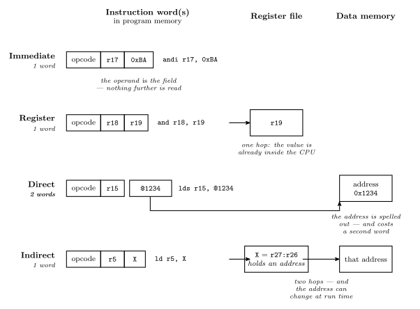
Figure 20: The four modes as one question: how far does the machine have to go to reach the operand? Immediate stops at the instruction itself. Register takes one hop, into the register file. Direct takes one hop into memory, but needs a second instruction word to carry the address. Indirect takes two hops and stays one word, and because its address lives in a register it can change while the program runs. The field splits shown inside the instruction words are schematic, not the real AVR encodings.
Figure 20 is the whole comparison in one line: immediate, register, direct, indirect is a list in increasing order of indirection, and every step down it either costs an instruction word or costs a hop through some storage on the way to the operand.
Immediate addressing
An operand value is in the instruction. andi r17, 0xBA carries 0xBA inside the instruction word itself — nothing is fetched from anywhere, the bits are the number. On AVR the immediate instructions are the ones whose mnemonic ends in i (ldi, andi, ori, cpi) and they pay for the immediate with encoding space: only four bits are left for the register, which is exactly why they reach r16–r31 only.
Register addressing
Only register numbers in the instruction. and r18, r19 names two registers and nothing else; the values are already inside the CPU. This is the cheapest mode there is — no memory access at all — and it is why the AVR is a load/store machine: no arithmetic or logic instruction touches memory, its operands are either registers (and r18, r19) or an immediate carried in the instruction word (andi r17, 0xBA). Anything in SRAM has to be loaded into a register first.
Direct addressing
Memory address is in the instruction. lds r15, $1234 spells the address out in full.
These AVR instructions occupy two instruction words (32 bits): sixteen bits are nowhere near enough for both an opcode and a 16-bit address, so the address gets a word of its own. That is the standing trade — a direct access is simple to read and needs no setup, but it costs double the program memory and cannot be computed at run time.
Indirect addressing
Memory address in register; register number is in the instruction. ld r5, X says “load from wherever X points”, and X is the pointer register pair of avr-architecture.
The instruction stays one word, because it only has to name which pointer. The address itself is data now, not code — which is what makes loops over arrays possible: increment the pointer and the same instruction reaches the next element.
Reading the trade-off
| Instruction words | Address decided | Costs | |
|---|---|---|---|
| Immediate | 1 | when you write the program | encoding space, hence ldi’s r16–r31 limit |
| Register | 1 | — | nothing; the value is already in the CPU |
| Direct | 2 | when you write the program | an extra program-memory word per access |
| Indirect | 1 | at run time | a pointer register, and loading it first |
The pattern: anything the instruction has to say costs instruction bits; anything it can point at costs a register and a setup step instead. Direct and indirect are the same access to the same memory cell — they differ only in which of those two prices you pay.
What the extra word does not cost
ld/st (indirect) are one instruction word, two cycles; lds/sts (direct) are two instruction words, two cycles. So direct addressing’s extra cost is paid entirely in program memory, not in time — both memory forms take the same two cycles, because both make one data-memory access and that access is what dominates.
For contrast, in/out use neither mode — they name an I/O register number directly in the instruction — and take one word, one cycle. That one-cycle figure is the reason in/out exist at all rather than everything going through lds/sts (avr-io-ports).
See also
- instruction-set-architecture — addressing modes as part of the “instructions” pillar
- avr-instructions —
ld/lds/st/stsand the immediate instructions - avr-architecture — the X, Y and Z pointer registers indirect mode uses
- memory-models — the address space being addressed
- 2026-09-03-instruction-set-architecture-part-2 — Lecture 12
AVR Architecture
The Atmel AVR: what is on the chip, how the CPU is laid out, and where the fetch-decode-execute cycle happens in it. See cpu-organisation for the generic picture this specialises and avr-instructions for what it executes.
Microcontroller, not microprocessor
Atmel AVR devices are microcontrollers. A microcontroller includes lots of components on one chip:
- CPU
- Memory (RAM)
- Program memory
- Input/output devices
That is the distinction from a microprocessor, which is the CPU alone. An ATmega324A is not a CPU — it contains a CPU, alongside memory and a large collection of peripherals, so that a useful system can be one chip rather than a board full of them.
The AVR CPU
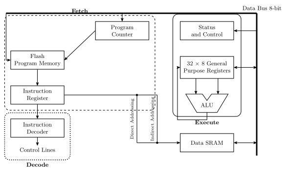
Figure 21: The AVR CPU core, with the three stages of the cycle marked. Fetch (dashed) reads the next instruction from flash under the program counter into the instruction register; decode (dotted) turns it into control lines; execute (solid) runs it over the register file, ALU and status register, with the 8-bit data bus tying everything together. The two lines dropping to the Data SRAM are the direct and indirect addressing routes — both come out of the instruction, which is why they leave from the instruction register. The execute group takes in the status register, the register file and the ALU; the Data SRAM sits outside it.
Reading the diagram as the cycle of fetch-decode-execute-cycle:
| Stage | Blocks involved |
|---|---|
| Fetch | Program Counter → Flash Program Memory → Instruction Register |
| Decode | Instruction Register → Instruction Decoder → Control Lines |
| Execute | General purpose registers → ALU → back to registers, with Status and Control updated |
Because these three groups are largely separate hardware, the AVR overlaps them: while one instruction executes, the next is being fetched. This course calls it a three-stage pipeline. The ATmega164A/324A/644A/1284P datasheet describes the core as “single level pipelining”, i.e. fetch and execute overlapping, which is two stages. Answer three-stage pipeline in the exam, but the datasheet is the authority on the hardware.
The pieces
| Block | Notes |
|---|---|
| Flash program memory | Holds the program. 32 kB on the ATmega324A, and non-volatile — it survives power loss |
| Program Counter | Addresses flash to select the next instruction — the PC of cpu-organisation |
| Instruction Register | Holds the instruction currently being worked on |
| Instruction Decoder | Turns the instruction’s bits into control lines — this is the control unit |
| 32 × 8 general purpose registers | R0–R31, each 8 bits wide, built from flip-flops |
| ALU | 8-bit, so AVR is an 8-bit machine |
| Status and Control | Holds the flags the ALU produces — N, Z, C, V among others |
| Data SRAM | 2 kB, volatile — static RAM, i.e. flip-flops |
| Data bus | 8 bits wide, tying the execute-side blocks together |
Two addressing routes reach the SRAM, drawn as the two vertical paths in Figure 21 — direct addressing (the address is in the instruction) and indirect addressing (the address is in a register). Both leave from the instruction register, because in either case it is the instruction that says which cell is wanted; they differ only in whether it says so with a literal address or with the name of a pointer. Both, and the other two modes, are in addressing-modes.
Four numbers define the chip: the flash is 32 kB and non-volatile; the SRAM is 2 kB, volatile, and made of static flip-flops; the register file is 32 registers, r0…r31, each 8 bits wide and made of flip-flops; and the ALU is 8-bit, which makes the AVR an 8-bit machine.
The register file
General purpose registers (0–31) are quite regular and can be used interchangeably. Two exceptions are worth having by heart:
- A few instructions work on half the registers (r16–r31), because only 4 bits are used to represent the operand in the instruction and \(2^4 = 16\).
LDI,SER,ANDI,ORIandCPIare among them — see avr-instructions. - X, Y and Z are register pairs that double as 16-bit pointers.
X, Y and Z
The top six registers of the file are those three pairs, low byte in the lower-numbered register:
| Pointer | High : Low | Register addresses |
|---|---|---|
| X | R27 : R26 | 0x1B : 0x1A |
| Y | R29 : R28 | 0x1D : 0x1C |
| Z | R31 : R30 | 0x1F : 0x1E |
Two 8-bit registers side by side make a 16-bit address — which is what the data space needs and no single 8-bit register can hold. They are what indirect addressing uses: ld r5, X means “load from wherever X points”, and the instruction only has to name which pointer, so it stays one word (addressing-modes).
The low byte living in the lower-numbered register is the same little-endian convention the AVR uses in memory (memory-models).
Address spaces
The AVR is a Harvard machine — separate address spaces for instructions and data — so 0x0000 names two entirely different locations depending on which space is meant, and the instruction decides.
Data address space — 0x0000 to 0x08FF
| Region | Addresses | Size |
|---|---|---|
| 32 Registers | 0x0000–0x001F |
32 |
| 64 I/O Registers | 0x0020–0x005F |
64 |
| 160 Ext I/O Reg. | 0x0060–0x00FF |
160 |
| Internal SRAM | 0x0100–0x08FF |
2048 bytes (2 kB) |
The register file and all 224 I/O registers are mapped into the data space, ahead of the SRAM. That is what lets lds/sts reach an I/O register by its data address while in/out reach the first 64 by their I/O register number — the two numbering systems differ by exactly the 0x20 the register file occupies. Details in avr-io-ports.
The datasheet draws the SRAM box as 1024/2048/4096/16384 × 8 because the diagram covers the whole ATmega164A/324A/644A/1284P family; the 324A is the 2048 entry, which is what puts the top of the data space at 0x08FF.
Program memory — 0x0000 to 0x3FFF
\(2^{14}\) 16-bit words: 16,384 instruction words = 32,768 bytes = 32 kB. The datasheet splits it into an Application Flash Section and, at the highest addresses, a Boot Flash Section.
0x3FFF \(= 2^{14} - 1\), and the sizing arithmetic — why 32 kB of program memory is 14 address bits rather than 15 — is worked through in memory-models. The short version: the cells are 16 bits wide, so there are half as many of them as there are bytes.
The AVR status register
8 bits, all readable and writable, all reset to 0:
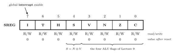
Figure 22: The status register, in the three-row form the datasheet uses: bit numbers above, flag names in the boxes, then the access row and the value each bit takes after reset. The callout names bit 7, the global interrupt enable; the braces underneath mark the four ALU flags and the sign flag \(S = N \oplus V\).
Instruction descriptions refer to these as SREG(n) by bit number:
| Flag | Bit | Meaning |
|---|---|---|
| C | SREG(0) | carry — was a carry out generated? |
| Z | SREG(1) | zero — was the result 0? |
| N | SREG(2) | negative — the sign bit of the result |
| V | SREG(3) | overflow — did a two’s complement addition/subtraction overflow? |
| S | SREG(4) | sign, \(= N \oplus V\) — the sign of the result corrected for any overflow |
| H | SREG(5) | half-carry — carry out of bit 3 |
| T | SREG(6) | transfer bit, used by BLD and BST |
| I | SREG(7) | global interrupt enable — set by sei, cleared by cli; cleared by the hardware when it takes an interrupt and set again by reti (avr-interrupts) |
C, Z, N and V are exactly the four flags of fetch-decode-execute-cycle.
S is not simply “the sign bit” — that is N. \(S = N \oplus V\) means: the result is negative (with no overflow), or would have been negative had overflow not occurred. That correction is what makes signed comparisons work, which is why the signed branches (BRLT, BRGE) test S while the unsigned ones (BRLO, BRSH) test C. The four cases — including the overflow case where N alone gives the wrong answer — are drawn in 2026-09-14-flow-of-control, and the branch pairs are tabulated in avr-branches-and-jumps.
The one-line meanings and the SREG(n) numbering are those of Atmel’s AVR Instruction Set Manual and the instruction summary in the ATmega324A datasheet. The I/O register map is the I/O register summary, pages 636–639 of the ATmega164A/324A/644A/1284P datasheet, which writes the I/O register number first and the data memory address in parentheses after it.
On-chip peripherals (ATmega324A)
Beyond the CPU and its memories, the chip carries a large set of peripherals — this is what makes it a microcontroller rather than a processor. The two figures nest: the whole of Figure 21 is what sits inside the single box marked AVR CPU in Figure 23.
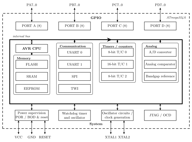
Figure 23: What is on the ATmega324A: the datasheet block diagram, rearranged into clusters by kind of thing — GPIO, memory, communication, timers/counters, analog and system. The dashed outline is the package boundary and the heavy rectangle inside it the internal bus, both as the datasheet draws them; the individual peripheral-to-port wiring is left out.
| Group | On the chip |
|---|---|
| General purpose I/O | PORT A, PORT B, PORT C, PORT D — four 8-bit ports |
| Communication | USART 0, USART 1, SPI, TWI |
| Timers/counters | 8-bit T/C 0, 16-bit T/C 1, 8-bit T/C 2 (T/C 3 is on the ATmega1284/1284P, not the 324A — the family datasheet’s block diagram covers both) |
| Analog | A/D converter, analog comparator, internal bandgap reference |
| Memory | Flash (program), SRAM (data), EEPROM (data, non-volatile) |
| System | Power supervision (POR/BOD & reset), watchdog timer and oscillator, oscillator/clock generation (XTAL1, XTAL2), JTAG/OCD |
There are three memories with three different jobs: flash for the program, SRAM for volatile working data, and EEPROM for data that must survive a power cycle. SRAM and EEPROM are the pair to keep straight: both hold data, and they differ only in surviving a power cycle.
See also
- cpu-organisation · fetch-decode-execute-cycle · instruction-set-architecture
- avr-instructions — the instruction set this hardware runs
- avr-io-ports — the I/O registers and the four GPIO ports
- avr-interrupts — the I bit, the vector table and the peripherals’ interrupt sources
- avr-timers-and-counters · avr-usart · avr-spi · analog-to-digital-conversion — four of the peripherals in detail
- memory-models · addressing-modes — the two address spaces, and how instructions name them
- assembly-process — flash, SRAM and EEPROM as the assembler’s three segments
- memory-technologies — flash, SRAM and EEPROM as technologies, and what the boot loader section is for · memory-hierarchy-and-cache — where the registers and SRAM sit by speed, and why the AVR needs no cache
- binary-number-representations — the flags’ two’s complement interpretation
- 2026-08-27-avr-introduction — Lecture 10
- 2026-08-31-instruction-set-architecture-part-1 — Lecture 11
AVR Branches and Jumps
How an AVR program’s control leaves the straight line: the ten conditional branches and which status flag each one reads, why greater than needs two different instructions for signed and unsigned bytes, the three unconditional jumps and how far each can reach, and the assembly idioms — if, if … else, counted and conditional loops — built from them. First met in 2026-09-14-flow-of-control, with the compare instructions and breq/brne first met in 2026-09-03-instruction-set-architecture-part-2. Procedure calls, the other way control moves, are in procedures-and-the-stack.
Flow of control
The flow of control is the sequence in which instructions actually execute. By default it is linear: every fetch-decode-execute cycle ends with \(PC \leftarrow PC + 1\) (fetch-decode-execute-cycle), so the next instruction is the next one in memory. Four kinds of instruction replace that increment with a new value:
| Decides | ||
|---|---|---|
| Branches | conditional | a status-register flag |
| Jumps | unconditional | nothing — always taken |
| Procedure calls and returns | unconditional, and they remember where they came from | procedures-and-the-stack |
| Interrupts / traps | triggered by hardware, not by an instruction | polling-and-interrupts · avr-interrupts |
Everything below is one instruction that writes the PC.
Conditional branches
A conditional branch tests one bit of the status register (avr-architecture) and, if the bit has the value the instruction wants, loads the PC with the address of a label; otherwise execution falls through to the next instruction. There is one instruction per flag per value:
| Branch if flag = | C | N | V | S = N ⊕ V | Z | T | H | I |
|---|---|---|---|---|---|---|---|---|
| 0 | brsh (= brcc) |
brpl |
brvc |
brge |
brne |
brtc |
brhc |
brid |
| 1 | brlo (= brcs) |
brmi |
brvs |
brlt |
breq |
brts |
brhs |
brie |
The first five columns are the ten branches counted above; the last three are the same pattern applied to the remaining flags and are in the instruction set reference. The mnemonics read as the condition, not the flag: brsh is branch if same or higher and happens to be branch if carry clear; brge is branch if greater or equal and happens to be branch if S clear. Learn them as conditions and the flags take care of themselves.
Every branch is relative and short. The offset is seven bits, so a conditional branch can reach only about 64 words either side of itself. For a farther target, branch on the opposite condition around a jmp:
    cp   r5, r6
    brne skip          ; opposite of the condition wanted
    jmp  far_away      ; taken only when r5 == r6
skip:
A taken branch costs two cycles, a not-taken one; the branch itself is one 16-bit word.
Setting the flags first
A branch reads flags; something has to have written them. Usually that is a compare (avr-instructions):
| Computes | Keeps | |
|---|---|---|
cp rd, rr |
rd − rr |
flags only |
cpi rd, K |
rd − K |
flags only — rd must be r16–r31 |
tst rd |
rd AND rd |
flags only — Z and N say whether rd is zero or negative |
but any ALU instruction sets flags, and a branch straight after an add, sub, dec or andi tests the result of that. dec r17 followed by brne loop is the standard loop counter, and no cp is needed. The rule from avr-program-structure holds either way: nothing that disturbs the flag may sit between the setter and the branch.
Signed and unsigned comparisons
Equality is the same question for signed and unsigned bytes, so breq and brne serve both. Ordering is not: whether 1111 1111 is bigger than 0000 0001 depends on whether it means 255 or −1, and the bits alone cannot say (binary-number-representations). The cp sets the same flags either way; the programmer chooses which pair of branches to read them with, and thereby declares the type:
Branch if rd ≥ rr |
Branch if rd < rr |
Reads | |
|---|---|---|---|
| unsigned | brsh — same or higher |
brlo — lower |
C: an unsigned subtraction needs a borrow exactly when the result went below zero |
| signed | brge — greater or equal |
brlt — less than |
S = N ⊕ V: the sign of the result, corrected for overflow |
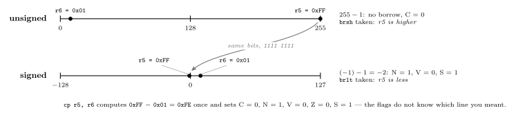
Figure 24: The same two bit patterns on the two number lines an 8-bit register can be read against. As unsigned values, 0xFF is 255 and sits at the far right, above 0x01; as two’s complement values it is \(-1\) and sits just left of zero, below 0x01. One cp r5, r6 produces one set of flags for both readings. The unsigned branches take their answer from the carry flag, which records whether the subtraction had to borrow; the signed branches take theirs from S, which is the sign of the difference with any overflow undone. Choosing brsh or brlt after the compare is the only place the program says which line it meant.
Why S and not N. N is the top bit of the 8-bit result. When a signed subtraction overflows — a large positive minus a large negative, say — the true difference does not fit in 8 bits, the stored result wraps, and its top bit is the opposite of the true sign. V is set in exactly that case. So \(S = N \oplus V\) is the true sign whether or not overflow happened, and one flag test decides < correctly across the whole range; the four cases are drawn in 2026-09-14-flow-of-control. In C none of this is visible: the compiler reads the variable’s declared type and emits brlo for unsigned char and brlt for char, the same way it picks lsr or asr for >> (c-operators).
Unconditional jumps
| Instruction | Target | Size | Cycles | Reach |
|---|---|---|---|---|
jmp label |
absolute address | 32-bit (two words) | 3 | anywhere in program memory |
rjmp label |
PC + signed offset | 16-bit | 2 | ±2 K words (12-bit offset, −2048 to +2047) |
ijmp |
the address held in Z | 16-bit | 2 | anywhere; the target is a run-time value |
jmp carries a full program-memory address — 14 bits for the ATmega324A’s 16 K words of flash — which does not fit beside an opcode in one 16-bit word, so it takes two words and an extra cycle. rjmp carries a 12-bit offset from the instruction’s own position in one word, one cycle less, and reaches ±2 K words; in a program of a few hundred instructions every jump is within range, and it is the normal choice. ijmp takes the destination from Z, the pointer register of addressing-modes, so a program can compute where to go — a jump table, or C’s switch. The assembler resolves labels to addresses or offsets for all three; the programmer writes the label.
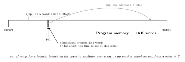
Figure 25: How far each kind of jump can reach from the instruction executing it. Program memory is the ATmega324A’s 16,K words; the marker is the current PC. A conditional branch carries a 7-bit offset and reaches about 64 words either way, an rjmp carries a 12-bit offset and reaches 2,K words either way, and a jmp carries the whole 14-bit address and reaches anywhere. The three are drawn to scale against the memory: the branch window is a sliver, the rjmp window covers a quarter of the chip, and the labs’ programs never leave either. The narrower the reach, the shorter and faster the instruction.
The idioms
Every C control structure (c-control-flow) compiles to a handful of these shapes. The branch is always on the opposite of the source condition, because what the branch does is skip the body.
if:
    cp   r5, r6
    brlt endif         ; skip the body when r5 < r6 (signed)
    ...                ; body: runs when r5 >= r6
endif:
if … else — the else part is the code the branch does not skip, and it needs a jmp past the if part:
    cp   r5, r6
    brge then
    ...                ; else part
    rjmp endif
then:
    ...                ; if part
endif:
while — test at the top, jump back at the bottom:
loop:
    cp   r5, r6
    brsh done          ; exit when r5 >= r6 (unsigned)
    ...                ; body
    rjmp loop
done:
Counted loop — count down to zero so the decrement sets Z for free:
    ldi  r17, 10       ; ten times
loop:
    ...                ; body
    dec  r17           ; sets Z when r17 reaches 0
    brne loop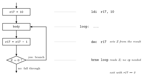
Figure 26: A counted loop, as a flowchart and as the four instructions that implement it. The counter is loaded once; the body runs; the decrement both updates the counter and sets the zero flag from the result; brne reads that flag and either returns to the label or falls out. Counting down rather than up saves the compare: dec leaves Z = 1 exactly when the counter has reached zero, so the branch tests the arithmetic directly. The body executes ten times, with r17 holding 10 down to 1 inside it and 0 on exit — the assembly form of for (i = 10; i != 0; i--).
Picking the branch. Write the C condition, decide signed or unsigned, and take the opposite instruction from the table:
| Source condition | Unsigned: skip with | Signed: skip with |
|---|---|---|
a == b |
brne |
brne |
a != b |
breq |
breq |
a < b |
brsh |
brge |
a >= b |
brlo |
brlt |
a > b |
swap operands: cp b, a then brsh |
cp b, a then brge |
a <= b |
cp b, a then brlo |
cp b, a then brlt |
There is no greater than branch; a > b is b < a, so compare the other way round.
See also
- avr-program-structure — labels, the template, and compare-then-branch drawn out
- procedures-and-the-stack —
call,rcall,icallandret: the jumps that come back - polling-and-interrupts — the fourth way the PC leaves its sequence, with no instruction asking
- avr-instructions —
cp,cpi,tst,dec, and which flags each instruction sets - avr-architecture — the status register; \(S = N \oplus V\)
- c-control-flow — the same shapes in C · binary-number-representations — signed and unsigned bytes
- assembly-process — how the assembler gives a label its address, counting each
jmpas two words - 2026-09-14-flow-of-control — Lecture 15 · 2026-09-03-instruction-set-architecture-part-2 — Lecture 12
AVR Instructions
The AVR instructions introduced so far, in assembly and in machine code. See instruction-set-architecture for what an instruction set is and avr-architecture for the hardware that runs these.
The full alphabetical instruction set — each mnemonic with its operation, description, flags affected, clock count, opcode pattern and an example — is in the AVR instruction set reference: Atmel’s AVR Instruction Set Manual, and the instruction summary in the ATmega324A datasheet the course says to keep open. The notation key immediately below and the per-instruction flag table at the end are unverified against that reference — check them against your own copy before leaning on them.
Reading the instruction set reference
Operand notation — how an operand’s allowed values map onto opcode bits:
| Notation | Meaning | Values | Opcode pattern |
|---|---|---|---|
Rd |
destination register (may be a source too) | r0…r31 | ddddd |
| r16…r31 | dddd (register number − 16) |
||
Rr |
source register | r0…r31 | rrrrr |
Rh:Rl |
register pair as a 16-bit quantity | r25:r24 / X / Y / Z | dd (00 / 01 / 10 / 11) |
K |
constant data | 0…255 | KKKKKKKK |
k |
constant address | −64…63, −2048…2047, 0…65535 | kkkkkkk … kkkk kkkk kkkk kkkk |
b |
bit number in a register | 0…7 | bbb |
s |
bit in the status register | 0…7 | sss |
P |
I/O register number | 0…63 | PPPPPP |
q |
displacement for direct addressing | 0…63 | qqqqqq |
The Rd row is the whole story behind LDI’s restriction — an instruction spending five bits on the register gets all 32; one spending four gets sixteen, and pays for it by starting at r16.
Operation notation — used in the Operation column:
M[a] / PM[a] / IO[a] |
SRAM cell / program memory (flash) byte / I/O register at address a |
PC / SP / STACK |
program counter / stack pointer / M[SP] |
← |
assigned value |
reg(a) |
bit a of register reg, numbered 7…0 most to least significant |
Flag names in the Flags Affected column are the SREG bits of avr-architecture.
Register conventions
Two operand names recur throughout the instruction set:
rd— the destination register.rr— the source register.
AVR is a two-operand machine: the destination is also one of the sources, so add rd, rr means rd ← rd + rr. (Contrast a three-operand ISA such as ARM, where add rd, r1, r2 leaves both sources untouched.) This matters when reading code — an AVR arithmetic instruction always overwrites one of its inputs.
Instructions by type
The instruction set can be cut two ways.
By what the instruction touches — the instruction-type list of instruction-set-architecture, filled in with the instructions so far:
| Type | Does | AVR so far |
|---|---|---|
| Input/Output | communicate with I/O devices/ports | IN, OUT |
| Load/Store | move data from/to memory | LD, LDS, ST, STS |
| Move | copy data between registers | MOV |
| Arithmetic | addition, subtraction, … | ADD, ADC, SUB, INC, NEG |
| Logical | Boolean operations | AND, ANDI, OR, ORI, EOR, COM |
| Branching | deciding which instruction to perform next | JMP, BREQ, BRNE |
By operand count, which splits the arithmetic and logical group instead:
| AVR examples | ||
|---|---|---|
| Dyadic | combine 2 operands to produce a result | add r5, r6 (arithmetic) · and r5, r6 (logical, bitwise) |
| Monadic | one operand → one result | ser r16 (set) · clr r5 (clear) · neg r5 (2’s complement) · com r5 (1’s complement) · the shifts and rotates |
The second cut is the one that predicts the syntax: a dyadic instruction has a comma in it, a monadic one does not.
The instructions so far
| Instruction | Meaning | Example |
|---|---|---|
MOV rd, rr |
copy contents of rr into rd — rd ← rr |
mov r3, r14 |
ADD rd, rr |
add contents of rr to rd — rd ← rd + rr |
add r5, r6 |
ADC rd, rr |
add with carry — rd ← rd + rr + C |
adc r11, r5 |
AND rd, rr |
bitwise AND, result into rd |
|
OR rd, rr |
bitwise OR, result into rd |
|
EOR rd, rr |
bitwise exclusive-OR, result into rd |
|
INC rd |
rd ← rd + 1 |
inc r22 |
LDI rd, number |
load immediate — put the number into rd |
ldi r16, 73 |
SER rd |
set all bits — rd ← $FF. Same as ldi rd, 0xFF, so r16–r31 only |
ser r17 |
CLR rd |
clear all bits — rd ← 0. Same as eor rd, rd, so any register |
clr r3 |
SUB rd, rr |
rd ← rd − rr |
sub r7, r19 |
COM rd |
one’s complement — flip all bits | com r8 |
NEG rd |
two’s complement — negate | neg r9 |
ANDI rd, K |
bitwise AND with a constant — r16–r31 only | andi r16, 0x01 |
ORI rd, K |
bitwise OR with a constant — r16–r31 only | ori r16, 0xF0 |
MOV is named misleadingly: it copies, it does not move. The source register is unchanged. It also affects no flags, which is what makes it safe to shuffle values between operations without disturbing the status register.
SER and CLR are short-hand ways of setting/clearing all bits of a register, and their restrictions differ because their expansions do:
| Exactly the same as | Reaches | |
|---|---|---|
ser rd (set register) |
ldi rd, 0xFF |
r16–r31 only — it inherits LDI’s four-bit register field |
clr rd (clear register) |
eor rd, rd |
any register, r0–r31 — EOR is a two-register instruction with five bits for each |
So clr r3 is legal and ser r3 is not, which looks arbitrary until you look at what each one assembles to. clr is also the reason \(X \oplus X = 0\) from bit-masking is worth remembering: XORing a register with itself is how the machine zeroes one.
Compare instructions
These do the arithmetic, discard the result, and keep only the flags — which is exactly what a conditional branch needs.
| Instruction | Does | Note |
|---|---|---|
CP rd, rr |
rd − rr |
compares two registers |
CPI rd, K |
rd − K |
compares against a constant — like ldi, r16–r31 only |
TST rd |
rd AND rd |
examines one register; literally the same operation as and rd, rd |
tst looks odd until you notice that ANDing a value with itself leaves it unchanged (\(X \cdot X = X\)) but still sets N and Z from it — so it is a zero/sign test that costs nothing and clobbers nothing. See bit-masking.
A comparison is the same as subtraction, with the result not saved — it exists only to set status register flags (Z, N, C, V …). And the instruction reference specifies which status register bits are set by which instructions: the flags are defined per instruction rather than falling out of one shared adder, which is the point of the table at the end of this note.
Branch instructions
Based on status register values — the flags a compare just set:
Branches to label if |
|
|---|---|
BREQ label |
Z = 1 |
BRNE label |
Z = 0 |
Together with CP that is a complete conditional: compare, which sets Z exactly when the two operands were equal, then branch on Z.
    cp   r5, r6          ; r5 - r6, result thrown away, flags kept
    breq same            ; Z = 1, i.e. r5 == r6
JMP label is the unconditional version — it tests nothing and always goes. Labels, and the program skeleton the branches live in, are in avr-program-structure.
breq/brne are two of ten: there is one branch per status flag per value, and the pairs that matter for ordering are brsh/brlo (unsigned, on C) and brge/brlt (signed, on S) — the full table, and why the signed pair reads S rather than N, are in avr-branches-and-jumps.
Control flow
The instructions that write the PC, and the two stack instructions that go with the calls (avr-branches-and-jumps, procedures-and-the-stack):
| Instruction | Does | Words | Cycles |
|---|---|---|---|
BRxx label |
branch if a flag has the wanted value; reach ±64 words | 1 | 1 (not taken) / 2 (taken) |
JMP label |
PC ← address of label |
2 | 3 |
RJMP label |
PC ← PC + offset; reach ±2 K words | 1 | 2 |
IJMP |
PC ← Z | 1 | 2 |
CALL label |
push the return address, then as JMP |
2 | 4 |
RCALL label |
push the return address, then as RJMP |
1 | 3 |
ICALL |
push the return address, then as IJMP |
1 | 3 |
RET |
pop the return address into PC | 1 | 4 |
PUSH rr |
store rr at SP, SP ← SP − 1 |
1 | 2 |
POP rd |
SP ← SP + 1, load rd from SP |
1 | 2 |
None of these touches the status register except by what the pushed and popped values happen to be; a call between a cp and its branch is safe only if the procedure preserves the flags, which in practice means it is not.
Three more belong to interrupts, and between them they are the only instructions that change the I bit (avr-interrupts):
| Instruction | Does | Words | Cycles |
|---|---|---|---|
SEI |
I ← 1: interrupts enabled | 1 | 1 |
CLI |
I ← 0: interrupts disabled | 1 | 1 |
RETI |
pop the return address into PC, and I ← 1 | 1 | 4 |
RETI is RET plus set I. A handler that ends in RET returns to the right place and leaves interrupts off for good.
Data movement
Data is usually copied, not moved — in every instruction below the source is left alone. What changes is where the two ends are:
| Direction | Called | AVR |
|---|---|---|
| register → register | move | mov |
| memory → register | load | lds, ld |
| register → memory | store | sts, st |
| I/O register → register | input | in |
| register → I/O register | output | out |
Three different places a value can live — a general purpose register, data memory, an I/O register — and a different instruction family for each. The one thing that is genuinely out of reach is SRAM from in/out: P only goes up to 0x3F, so those two never leave the first 64 I/O registers.
Everything else is a question of cost and numbering, not reachability. Because the I/O registers are mapped into the data space (avr-io-ports), lds/sts can reach one — in r16, 0x09 and lds r16, 0x29 both read PIND, the second for two instruction words instead of one. The bug to actually watch for is writing the I/O register number where the data address belongs, or the reverse.
Load and store
| Does | Addressing | Words | Cycles | |
|---|---|---|---|---|
LD rd, X |
rd ← Mem[X] |
indirect — address in the pointer register | 1 | 2 |
ST X, rr |
Mem[X] ← rr |
indirect | 1 | 2 |
LDS rd, k |
rd ← Mem[k] |
direct — 16-bit address in the instruction | 2 (32 bits) | 2 |
STS k, rr |
Mem[k] ← rr |
direct | 2 | 2 |
For example:
    ld   r5, X           ; r5 <- Mem[X]
    st   X, r5           ; Mem[X] <- r5
    lds  r5, 0x20        ; r5 <- Mem[0x20]
    sts  0x20, r5        ; Mem[0x20] <- r5
Both pairs reach the same data space — the difference is only where the address comes from (addressing-modes), and lds/sts pay a second instruction word for spelling it out. X here is the pointer pair of avr-architecture.
In and out
| Does | Words | Cycles | |
|---|---|---|---|
IN rd, P |
rd ← I/O register P |
1 | 1 |
OUT P, rr |
I/O register P ← rr |
1 | 1 |
rd/rr may be any of r0–r31 — unlike ldi, these are not restricted to the top half — and P is an I/O register number 0–63 (0x00–0x3F) or a name from m324Adef.inc. Examples: in r5, 0x26 (I/O register 0x26 is TCNT0) and out PORTD, r6. Full treatment in avr-io-ports.
One word and one cycle makes these the cheapest access on the chip — cheaper than reaching the very same register through lds/sts, which is the whole reason the first 64 I/O registers are special.
Shifts and rotates
Monadic instructions that move every bit one place. They differ only in what arrives at the vacated end and what happens to the bit that falls off — and in all five, the bit that falls off lands in C.
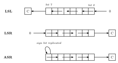
Figure 27: The three shift instructions. LSL and LSR feed a 0 into the vacated end; ASR feeds the sign bit back into itself, which is what makes it a signed division. In all three the bit shifted out lands in the carry flag.
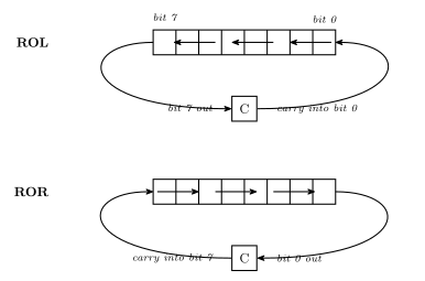
Figure 28: The two rotate instructions. A rotate is a shift whose vacated end is fed from the carry flag instead of a constant, so the register and C together behave as a nine-bit ring.
| Name | Into the vacated end | Out | |
|---|---|---|---|
LSL rd |
Logical Shift Left | 0 → bit 0 |
bit 7 → C |
LSR rd |
Logical Shift Right | 0 → bit 7 |
bit 0 → C |
ASR rd |
Arithmetic Shift Right | bit 7 replicated into itself | bit 0 → C |
ROL rd |
ROtate Left through carry | C → bit 0 | bit 7 → C |
ROR rd |
ROtate Right through carry | C → bit 7 | bit 0 → C |
What they compute
Shifting a binary number one place is multiplying or dividing it by two, which is the whole reason these exist. Using four bits for legibility:
| Worked example | ||
|---|---|---|
LSL |
× 2 | 0010 (2) → 0100 (4) → 1000 (8) |
LSR |
÷ 2, read unsigned | 0110 (6) → 0011 (3); 1000 (8 unsigned) → 0100 (4) |
ASR |
÷ 2, read signed | 1000 (\(-8\)) → 1100 (\(-4\)) |
LSR and ASR are the pair to keep straight. Given 1000, LSR produces 0100 — right if the value meant unsigned 8, wrong if it meant \(-8\). ASR replicates the sign bit into the vacated position and produces 1100 \(= -4\). The same bits go in; the instruction is where you declare which interpretation you meant (binary-number-representations).
There is no matching pair going the other way, because left shifts need no such distinction: a 0 always enters at the bottom, and the signed and unsigned readings of “× 2” agree — right up until the result stops fitting in eight bits.
Shifting a value wider than eight bits
Rotates exist to carry a bit from one byte into the next. To multiply the 16-bit unsigned value in r13:r14 by two (so r13 is the high byte, r14 the low):
    lsl  r14             ; low byte x2; bit 7 falls out into C
    rol  r13             ; high byte x2, pulling C into its bit 0
LSL on the low byte pushes its top bit into C; ROL on the high byte pulls exactly that bit back in at the bottom. The two instructions together shift a sixteen-bit quantity one place.
The wrong answers are worth naming, because each fails differently. lsl r13 (and asl r13, which is the same operation under another name — shifting left, a 0 always enters) shifts the high byte but feeds it a 0, discarding the bit the low byte just produced. rol r14 rotates the wrong byte.
Building wider operations from 8-bit ones
The AVR supports exactly one data type in hardware — an 8-bit integer (instruction-set-architecture). Everything wider is a sequence of instructions, and C is what stitches the pieces together.
Add the 16-bit quantity r5:r4 to r11:r10, result in r11:r10 — high byte named first, so r4 and r10 are the low bytes:
    add  r10, r4         ; r10 <- r10 + r4        (low bytes; carry out lands in C)
    adc  r11, r5         ; r11 <- r11 + r5 + C    (high bytes, plus that carry)
ADD on the low bytes leaves any carry out of bit 7 in C, and ADC on the high bytes adds it back in — the same column-by-column carrying as long addition on paper, one byte per column.
The order is not negotiable, and neither is what sits between the two lines: adc has to run after the add that produced the carry, and any instruction in between that touches C ruins the result. That is the general shape of multi-byte arithmetic on an 8-bit machine — low end first, and nothing allowed to disturb the flag in the middle.
Constants
Constants do not have to be hexadecimal. All five of these load the same value into r17:
| Written | Radix | |
|---|---|---|
ldi r17, 0x34 |
hexadecimal | 0x prefix |
ldi r17, $34 |
hexadecimal | $ prefix |
ldi r17, 52 |
decimal | no prefix |
ldi r17, 064 |
octal | a leading 0 |
ldi r17, 0b00110100 |
binary | 0b prefix |
\(\texttt{0x34} = 52 = 64_8 = \texttt{0b00110100}\). The octal form is the trap: a leading zero changes the radix, so 012 is 10, not 12.
LDI’s restrictions
LDI is the one with strings attached:
- Registers r16 to r31 only. Not r0–r15.
- 8-bit numbers,
00000000to11111111. Written in decimal the range is \(-128\) to \(255\) — that span covers both the signed and the unsigned reading of eight bits.
A counter-example, and the legal version of it:
    ldi  r0, 5           ; NOT legal - r0 is below r16
    ldi  r16, 5          ; the same idea, in a register ldi can reach
The register restriction is not arbitrary: it falls straight out of the encoding below, which has only four bits for the register number.
Machine code
Each instruction is a 16-bit word made of an opcode and operand bit fields — see instruction-set-architecture. In the AVR datasheet’s notation, a format like 0000 11rd dddd rrrr means the literal bits are fixed and each letter is one bit of an operand, gathered from wherever it appears.
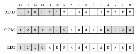
Figure 29: Three AVR instruction encodings, each 16 bits. Fixed opcode bits are shaded; letters are operand bits. In ADD and LDI the operand bits are not contiguous — the register number’s top bit sits apart from the rest, and LDI’s constant is split into two nibbles either side of the register field.
ADD — 0000 11rd dddd rrrr
The opcode is bits 15–10, 0000 11 — six fixed bits, all that is left once the two five-bit register numbers have taken ten of the sixteen. The destination register number is d dddd — five bits, so all 32 registers — and the source is r rrrr. Both have their top bit separated from the other four, and note the order in the middle nibble: the source’s top bit (r, bit 9) comes before the destination’s (d, bit 8), even though the mnemonic writes the destination first.
Worked example: add r23, r7.
| Register | In binary (5 bits) | Split as | |
|---|---|---|---|
rd |
r23 = 16 + 4 + 2 + 1 | 10111 |
d = 1, dddd = 0111 |
rr |
r7 = 4 + 2 + 1 | 00111 |
r = 0, rrrr = 0111 |
Dropping those into 0000 11rd dddd rrrr:
\[\texttt{0000 1101 0111 0111}\]
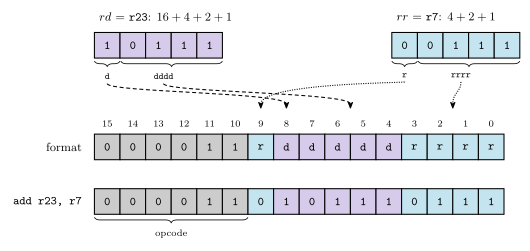
Figure 30: Assembling add r23, r7. Each register number is written as five bits, then torn in two: the top bit goes into the middle nibble and the low four into their own field. Shading, not position, is what tells the two operands apart here. The two guide lines cross because the destination’s bit sits between the source’s two pieces.
COM — 1001 010d dddd 0000
Flip all bits — one’s complement. One register operand, again as d dddd.
Worked example: com r19. r19 = 16 + 2 + 1 = 10011, so d = 1 and dddd = 0011:
\[\texttt{1001 0101 0011 0000}\]
LDI — 1110 KKKK dddd KKKK
Two operand fields:
K— the 8-bit constant, split into two nibbles: the high four bits in the firstKKKKfield, the low four in the last.d— the register number minus 16.
That subtraction is why LDI only reaches r16–r31: the field is four bits, so it can express \(2^4 = 16\) distinct registers, and the ISA spends them on the top half of the register file.
Applying the rule to ldi r16, 73: \(d = 16 - 16 = 0\), so dddd = 0000; \(73 = \texttt{0100 1001}\), so the high nibble is 0100 and the low nibble 1001:
\[\texttt{1110 0100 0000 1001}\]
Flags, by instruction
The reference’s Flags Affected column is worth reading rather than assuming — the flags are defined per instruction, not derived from a single adder. For the instructions above:
| Instruction | Z | C | N | V |
|---|---|---|---|---|
MOV, LDI, SER |
— | — | — | — |
AND, ANDI, OR, ORI, EOR, TST |
from result | unchanged | from result | cleared to 0 |
ADD, ADC, SUB, CP, CPI |
from result | from carry/borrow | from result | signed overflow |
CLR |
always 1 | unchanged | always 0 | cleared to 0 |
COM |
from result | always set to 1 | from result | cleared to 0 |
NEG |
from result | set unless the result is $00 |
from result | set only if the result is $80 |
Two of these will catch you out. The logical operations leave C alone entirely — whatever it held before an and it still holds after. And COM sets C unconditionally, which is not a carry out of anything; it is a defined convention, chosen so that com followed by an increment behaves like a negation.
The CLR row is just the logical row with a result that is guaranteed to be 0x00 — clr rd is eor rd, rd — which makes it the one instruction whose flags you can predict without knowing the operand.
For the shift, rotate and branch instructions, look the flags up in the reference rather than guessing. The one part that is visible in the diagrams above is C: every shift and rotate sets it from the bit that fell out. The rest is defined per instruction, as the paragraph opening this section warns.
For ADD specifically, the manual gives the flags as Boolean formulas over the operand and result bits, writing \(R\) for the result (which equals Rd after the operation):
\[N = R_7 \qquad Z = \overline{R_7}\cdot\overline{R_6}\cdot\overline{R_5}\cdot\overline{R_4}\cdot\overline{R_3}\cdot\overline{R_2}\cdot\overline{R_1}\cdot\overline{R_0}\] \[V = Rd_7 \cdot Rr_7 \cdot \overline{R_7} + \overline{Rd_7}\cdot\overline{Rr_7}\cdot R_7 \qquad C = Rd_7 \cdot Rr_7 + Rr_7 \cdot \overline{R_7} + \overline{R_7}\cdot Rd_7\]
\(Z\) is a NOR over every result bit. \(V\) says overflow happened exactly when both operands had the same sign and the result’s differs — two negatives giving a positive, or two positives giving a negative. And \(S = N \oplus V\), for signed tests. See avr-architecture.
See also
- instruction-set-architecture · avr-architecture · bit-masking
- avr-io-ports — the I/O registers
in/outreach - addressing-modes — the four ways an operand names its value
- avr-program-structure — labels,
jmpand the program skeleton - avr-interrupts —
sei,cli,reti, and which flags an interrupt handler must save - binary-number-representations — one’s and two’s complement, and the \(-128\) to \(255\) range
- 2026-08-27-avr-introduction — Lecture 10
- 2026-09-03-instruction-set-architecture-part-2 — Lecture 12
AVR Interrupts
How the ATmega324A implements interrupts, and how to write one and switch it on, in assembly and in C: the path from a device’s request to the handler and back, the vector table, the switches that decide whether a request is taken, the ISR template and its stack, ISR() and the _vect names, volatile, priority, and a complete timer-interrupt program. First met in 2026-09-21-interrupts. What an interrupt is on any CPU (polling versus interrupts, the fourteen-step sequence, transparency, nesting) is polling-and-interrupts.
The path of an interrupt
An interrupt is a procedure call the hardware makes (procedures-and-the-stack). The CPU finishes the instruction in progress, pushes the address of the next one, turns interrupts off and loads the PC with the address of the vector table entry for the source. The entry holds a jmp to the handler. The handler ends with reti, which pops the return address and turns interrupts back on.
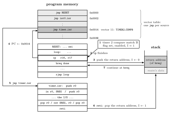
Figure 31: One timer interrupt from start to finish. The request (1) arrives while cp is executing, and the CPU lets it finish (2): an AVR instruction is never abandoned halfway. The hardware then pushes the address of the next instruction, breq, clears the I bit (3), and loads the PC with 0x0014 (4), the vector table entry for Timer/Counter 2 compare match B. The jmp stored there reaches the handler (5), which saves what it uses, does its work, restores, and ends with reti (6). That pops the return address and sets I again, and execution continues at breq (7) as if nothing had happened. It will, provided the handler restored the status register, because breq is about to read the Z flag that cp set. Nothing in the main program refers to the handler; the vector table is the only link between them.
The vector table
The first addresses of program memory hold the interrupt vector table: one entry per interrupt source, in a fixed order, each a two-word jmp to that source’s handler (avr-branches-and-jumps). The AVR uses a table of jump instructions, not a table of addresses. When it takes an interrupt it loads the PC with the address of the entry itself and executes what it finds there. So:
\[\text{entry address} = 2 \times (\text{vector} - 1)\]
RESET is vector 1, at 0x0000. A reset is taken through the same table as an interrupt, which is why every program begins with jmp RESET (avr-program-structure). The table has 31 entries on the ATmega324A and ends at 0x003C, so the program proper starts at 0x003E.
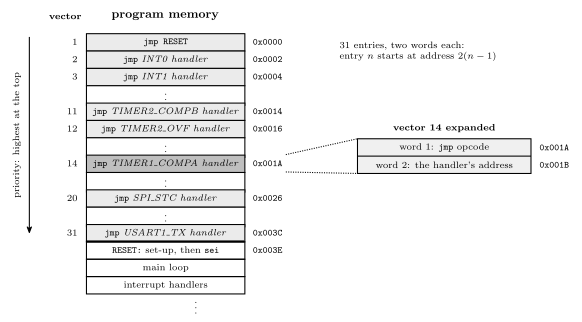
Figure 32: The bottom of program memory. Each vector-table entry is two words, the two halves of a jmp, so entry \(n\) sits at address \(2(n-1)\), and the table’s order is also its priority order: when two requests are waiting, the one nearer the top is taken first. The expanded entry shows what one of them holds, taking vector 14, Timer/Counter 1 compare match A, as the example. An entry for a source the program does not use can hold anything, as long as that interrupt is never enabled. The program itself starts at the first address after the table, which the jmp in entry 1 reaches at reset.
The full table for the ATmega324A, from pages 69–70 of the datasheet. The Group column sorts the sources by kind: GPIO, T/C, Comms, analog and system. The C name is the Source followed by _vect.
| Vector | Address | Source | Interrupt definition | Group | C handler |
|---|---|---|---|---|---|
| 1 | 0x0000 |
RESET |
RESET, watchdog reset, etc. | — | — (the program’s start) |
| 2 | 0x0002 |
INT0 |
External Interrupt Request 0 | GPIO | ISR(INT0_vect) |
| 3 | 0x0004 |
INT1 |
External Interrupt Request 1 | GPIO | ISR(INT1_vect) |
| 4 | 0x0006 |
INT2 |
External Interrupt Request 2 | GPIO | ISR(INT2_vect) |
| 5 | 0x0008 |
PCINT0 |
Pin Change Interrupt Request 0 (port A) | GPIO | ISR(PCINT0_vect) |
| 6 | 0x000A |
PCINT1 |
Pin Change Interrupt Request 1 (port B) | GPIO | ISR(PCINT1_vect) |
| 7 | 0x000C |
PCINT2 |
Pin Change Interrupt Request 2 (port C) | GPIO | ISR(PCINT2_vect) |
| 8 | 0x000E |
PCINT3 |
Pin Change Interrupt Request 3 (port D) | GPIO | ISR(PCINT3_vect) |
| 9 | 0x0010 |
WDT |
Watchdog Time-out Interrupt | system | ISR(WDT_vect) |
| 10 | 0x0012 |
TIMER2_COMPA |
Timer/Counter2 Compare Match A | T/C | ISR(TIMER2_COMPA_vect) |
| 11 | 0x0014 |
TIMER2_COMPB |
Timer/Counter2 Compare Match B | T/C | ISR(TIMER2_COMPB_vect) |
| 12 | 0x0016 |
TIMER2_OVF |
Timer/Counter2 Overflow | T/C | ISR(TIMER2_OVF_vect) |
| 13 | 0x0018 |
TIMER1_CAPT |
Timer/Counter1 Capture Event | T/C | ISR(TIMER1_CAPT_vect) |
| 14 | 0x001A |
TIMER1_COMPA |
Timer/Counter1 Compare Match A | T/C | ISR(TIMER1_COMPA_vect) |
| 15 | 0x001C |
TIMER1_COMPB |
Timer/Counter1 Compare Match B | T/C | ISR(TIMER1_COMPB_vect) |
| 16 | 0x001E |
TIMER1_OVF |
Timer/Counter1 Overflow | T/C | ISR(TIMER1_OVF_vect) |
| 17 | 0x0020 |
TIMER0_COMPA |
Timer/Counter0 Compare Match A | T/C | ISR(TIMER0_COMPA_vect) |
| 18 | 0x0022 |
TIMER0_COMPB |
Timer/Counter0 Compare Match B | T/C | ISR(TIMER0_COMPB_vect) |
| 19 | 0x0024 |
TIMER0_OVF |
Timer/Counter0 Overflow | T/C | ISR(TIMER0_OVF_vect) |
| 20 | 0x0026 |
SPI_STC |
SPI Serial Transfer Complete | Comms | ISR(SPI_STC_vect) |
| 21 | 0x0028 |
USART0_RX |
USART0 Receive Complete | Comms | ISR(USART0_RX_vect) |
| 22 | 0x002A |
USART0_UDRE |
USART0 Data Register Empty | Comms | ISR(USART0_UDRE_vect) |
| 23 | 0x002C |
USART0_TX |
USART0 Transmit Complete | Comms | ISR(USART0_TX_vect) |
| 24 | 0x002E |
ANALOG_COMP |
Analog Comparator | analog | ISR(ANALOG_COMP_vect) |
| 25 | 0x0030 |
ADC |
ADC Conversion Complete | analog | ISR(ADC_vect) |
| 26 | 0x0032 |
EE_READY |
EEPROM Ready | system | ISR(EE_READY_vect) |
| 27 | 0x0034 |
TWI |
2-wire Serial Interface | Comms | ISR(TWI_vect) |
| 28 | 0x0036 |
SPM_READY |
Store Program Memory Ready | system | ISR(SPM_READY_vect) |
| 29 | 0x0038 |
USART1_RX |
USART1 Receive Complete | Comms | ISR(USART1_RX_vect) |
| 30 | 0x003A |
USART1_UDRE |
USART1 Data Register Empty | Comms | ISR(USART1_UDRE_vect) |
| 31 | 0x003C |
USART1_TX |
USART1 Transmit Complete | Comms | ISR(USART1_TX_vect) |
Every timer event the course uses has its own vector. The three units’ compare matches and overflows are vectors 10–19, and a unit’s compare A and compare B are separate sources with separate handlers, just as they have separate flags (avr-timers-and-counters).
When a request is taken
Four things have to be true before a source’s handler runs. The four setup steps (set up the conditions, enable the interrupt, clear its flag, enable globally) arrange for them:
- The conditions for the interrupt are set up, so that the event can happen at all: a timer running in the right mode, or a pin configured to sense an edge.
- That particular interrupt is enabled, by its own bit in an I/O register. There is one bit per source.
- Its flag is set. The hardware does this when the event occurs, whether or not the interrupt is enabled. That is why the third setup step clears the flag before the interrupt is enabled: afterwards only a fresh event can set it, and an event from before the setup does not fire at once. Clearing is done by writing a 1 to the flag’s bit.
- Interrupts are enabled globally: the I bit of the status register is 1.
sei(orsei()in C) sets it.
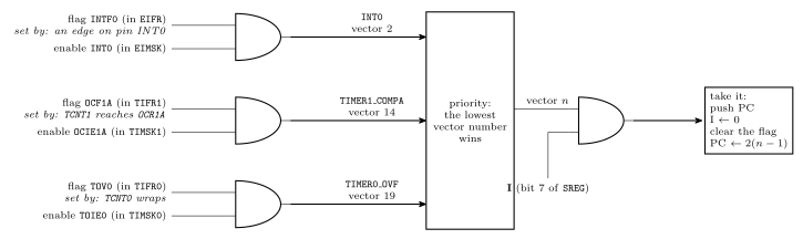
Figure 33: Whether a request becomes an interrupt, drawn as the logic it amounts to. Each source has a flag, set by its event, and an enable bit, set by the program. The source requests an interrupt only while both are 1, and all three sources here are gated the same way. If more than one is requesting, the lowest vector number wins. The winner is taken only if the I bit is also 1, and taking it clears I. For these sources, taking the vector also clears the flag. So a flag with its enable bit off simply stays set, available to be polled, and a flag that goes up while I is 0 waits and is taken the moment I returns to 1.
For the sources the course meets, the bits are:
| Source | Flag (register) | Enable (register) | Conditions set up in |
|---|---|---|---|
INT0 (pin PD2) |
INTF0 (EIFR) |
INT0 (EIMSK) |
EICRA: bits ISC01, ISC00 choose low level 00, any change 01, falling edge 10 or rising edge 11 |
TIMER0_COMPA |
OCF0A (TIFR0) |
OCIE0A (TIMSK0) |
TCCR0A, TCCR0B, OCR0A |
TIMER0_OVF |
TOV0 (TIFR0) |
TOIE0 (TIMSK0) |
TCCR0A, TCCR0B |
TIMER1_COMPA |
OCF1A (TIFR1) |
OCIE1A (TIMSK1) |
TCCR1A, TCCR1B, OCR1A |
TIMER1_OVF |
TOV1 (TIFR1) |
TOIE1 (TIMSK1) |
TCCR1A, TCCR1B |
The naming pattern is regular: an F for the flag and an IE for interrupt enable, with OC for output compare and TOV/TOIE for timer overflow. Each of these flags is cleared automatically when its vector is taken, so a handler does not normally clear its own flag. A program that polls a flag instead, with the interrupt left disabled, must clear it itself (avr-timers-and-counters).
The I bit
| I | Also | |
|---|---|---|
sei |
← 1 | |
cli |
← 0 | |
| taking an interrupt (hardware) | ← 0 | pushes PC, loads the vector address |
reti |
← 1 | pops PC |
I is bit 7 of SREG (avr-architecture), and it is 0 after reset, so no interrupt happens until the program executes sei. Because the hardware clears it on entry, a handler runs with interrupts off unless it turns them back on itself.
External interrupts
An external interrupt is requested by a pin. The ATmega324A has three, each fixed to one pin:
| Interrupt | Pin |
|---|---|
INT0 |
PD2 |
INT1 |
PD3 |
INT2 |
PB2 |
What the pin has to do to make a request is chosen by two sense control bits per interrupt, in EICRA:
ISCn1:0 |
A request is made |
|---|---|
00 |
for as long as the pin is low |
01 |
on any change of the pin |
10 |
on a falling edge, 1 to 0 |
11 |
on a rising edge, 0 to 1 |
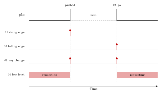
Figure 34: What each sense control setting responds to, for a push button that reads 1 while it is held. A rising edge is the moment the button is pushed and a falling edge is the moment it is let go. Any change gives a request at both. The low level setting is different in kind: it asks for the whole time the pin is low, so the handler runs again and again until the pin goes high.
Setting one up follows the same steps as any other interrupt. For a rising edge on INT0 and a falling edge on INT1:
ISR(INT0_vect) { /* PD2 went from 0 to 1 */ }
ISR(INT1_vect) { /* PD3 went from 1 to 0 */ }

/* in main */
EICRA = (1<<ISC01) | (1<<ISC00) | (1<<ISC11);   /* INT0 rising, INT1 falling */
EIMSK = (1<<INT0) | (1<<INT1);                  /* enable both               */
EIFR  = (1<<INTF0) | (1<<INTF1);                /* clear both flags          */
sei();- Edges fit buttons. An edge happens once per push, however long the button is held. That makes an external interrupt a natural way to act on a push or on a release without the program having to remember what the button was doing last time.
- Bounce. A mechanical contact chatters for a moment as it closes, and each chatter is an edge. One push can then run the handler several times.
- The low level setting keeps asking. If the pin is still low when the handler returns, the interrupt is taken again straight away.
- Priority.
INT0,INT1andINT2are vectors 2, 3 and 4, directly after reset, so they come before every timer and serial interrupt.
Used for the start/stop and reset buttons of a stopwatch in week9-lab-avr-interrupts.
Writing an ISR in assembly
The template:
isr_label:
    push r0              ; save r0: it is about to carry SREG
    in   r0, SREG
    push r0              ; save the interrupted program's flags

    ; ... perform the operation, usually input/output ...
    ; (any other register used: push it here, pop it below)

    pop  r0
    out  SREG, r0        ; flags back as they were
    pop  r0              ; r0 back as it was
    reti                 ; pop PC and set I
SREG cannot be pushed directly, because push takes a general-purpose register. So one register carries it, and that register is saved first. The restore is the save in reverse. Two consequences follow from where the save happens:
- The flags saved are the interrupted program’s. Apart from I, the hardware does not touch them on entry, and
pushchanges none, so the copy is exactly what the interrupted code left. - The saved I bit is 0, because the hardware cleared it before the first instruction of the ISR. Writing the copy back therefore leaves interrupts off until
reti, which is the right moment for them to come back.
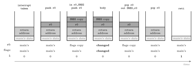
Figure 35: The stack through the ISR template, with the three things the interrupted program relies on (r0, its flags, and the I bit) traced underneath. The hardware’s push of the return address comes first, then the template’s two pushes, the SREG copy on top. The body is free to change r0 and the flags because both are safely on the stack. The restore pops the copy into r0 and writes it to SREG, then pops r0’s own value. When reti runs, the return address is on top again, exactly as the hardware left it. I stays 0 from entry to reti, the copy in the middle included, and it is reti that sets it.
Which registers to save is decided by what the body does. Save any register the body writes. Save SREG if any instruction in the body changes a flag, which rules in arithmetic, logic, compares and shifts but not in, out, ldi, mov, push or pop (avr-instructions). A handler that only copies a port to another port needs one register and no SREG at all (worked in 2026-09-21-interrupts).
Placing the entry in the table
The template in avr-program-structure puts jmp RESET at 0x0000 and leaves a comment where the handlers go. Once a vector is used, its jmp has to sit at exactly that vector’s address. The assembler’s .org directive sets the address of whatever comes next (assembly-process):
.include "m324Adef.inc"

.org 0x0000
        jmp  RESET
.org 0x001A              ; vector 14: TIMER1_COMPA
        jmp  timer1_compa_isr
.org 0x003E              ; first address after the table
RESET:
        ; stack pointer, ports, timer 1, TIMSK1 ...
        sei
loop:
        ; ...
        rjmp loop

timer1_compa_isr:
        push r0
        in   r0, SREG
        push r0
        ; ...
        pop  r0
        out  SREG, r0
        pop  r0
        reti
An assembly program that uses interrupts must also set up the stack pointer before the first sei (procedures-and-the-stack), since taking an interrupt pushes the return address.
Writing an ISR in C
#include <avr/interrupt.h>

ISR(INT0_vect) {
    /* code here */
}
ISR is a macro from avr/interrupt.h, and its argument names the vector: the source name from the datasheet followed by _vect (the table above). From it the compiler does everything the assembly programmer does by hand. The vector table is set up automatically: the handler’s jmp goes in the right entry. Registers are saved and restored automatically, SREG included, and the function ends in reti. What ISR() does not do is any of the four setup steps. In C, as in assembly, the program still sets up the conditions, enables the interrupt, clears its flag and calls sei(). sei() and cli() are macros for the single instructions.
A complete example
Timer 1 in CTC mode, matching eight times a second, with the handler toggling an LED and counting ticks. The timer set-up is Lab 12’s (week8-lab-avr-timers): \(8\,\text{MHz} / (64 \times 15625) = 8\ \text{Hz}\).
#include <avr/io.h>
#include <avr/interrupt.h>

volatile uint8_t ticks = 0;            /* written by the ISR, read by main */

ISR(TIMER1_COMPA_vect) {
    PORTA ^= (1<<0);                    /* toggle the LED on PA0 */
    ticks++;
}

int main(void) {
    DDRA = (1<<0);                      /* PA0 is an output */

    /* 1. conditions: CTC mode, clock/64, match at 15624 */
    OCR1A  = 15624;
    TCCR1A = 0;
    TCCR1B = (1<<WGM12) | (1<<CS11) | (1<<CS10);

    /* 2 and 3. clear any stale match, then enable this interrupt */
    TIFR1  = (1<<OCF1A);
    TIMSK1 = (1<<OCIE1A);

    /* 4. enable interrupts globally */
    sei();

    while (1) {
        if (ticks >= 8) {               /* a second has gone by */
            ticks = 0;
            /* ... once-a-second work ... */
        }
        /* ... anything else: the LED keeps time by itself ... */
    }
}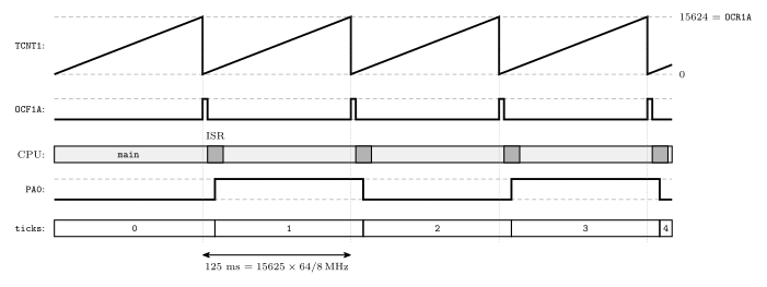
Figure 36: The example program running, one trace per signal. The count climbs to OCR1A = 15624 and is cleared (CTC mode), once every 125 ms. Each match sets OCF1A; the interrupt is enabled and I is 1, so the vector is taken a few cycles later, and taking it clears the flag again. The handler is a sliver of time in which the LED output is toggled and ticks counted, and the rest of the time belongs to main. Nothing in main looks at the timer. The LED blinks at 4 Hz, one toggle per match, however busy main is.
Priority
Priority is determined by vector: the lowest vector is the highest priority. RESET is highest, then INT0, and so on down the table. On the AVR, priority only matters when two or more interrupts are waiting to be serviced, and it decides which is taken first. It never lets one interrupt cut into another’s handler, because I is 0 throughout a handler. The datasheet adds one rule: after reti, the CPU always executes one instruction of the interrupted program before taking the next waiting interrupt, so a stream of interrupts can slow main down but never stop it altogether.
Interrupts can be re-enabled inside a handler with sei. Any incoming or waiting interrupt may then be serviced immediately, nested inside the current handler, even if it has lower priority. Priority plays no part there. Both cases are traced in 2026-09-21-interrupts and set against true priority nesting in polling-and-interrupts.
Pitfalls
- Forgetting
sei(). Everything else is set up, and nothing ever happens, because I is 0 from reset. - Enabling an interrupt that has no handler. In C, avr-libc fills every unused vector with a jump to a default handler that jumps to address 0, so the program restarts whenever the event occurs. It is not a true reset: the I/O registers keep whatever they held, which can make the restart behave differently from a power-up.
- Misspelling the vector name.
ISR(TIMER1_COMPA_Vect)compiles with only a warning, and the handler is never placed in the table, which makes it the previous pitfall. - Not clearing a stale flag before enabling: the interrupt fires once immediately, for an event that happened before the program was ready.
- Clearing a flag with
|=. If the compiler turns it into a read, an OR and a write, it clears every flag in the register that happens to be set (avr-timers-and-counters). Writing just the one bit,TIFR1 = (1<<OCF1A);, is safe however it is compiled. - In assembly: not saving
SREG, unbalanced pushes and pops, orretinstead ofreti. The first corrupts the interrupted code’s flags. The second returns to the wrong address. The third returns correctly but leaves I at 0, so no interrupt ever happens again. - Long handlers. No delay loops and no waiting inside an ISR: every other interrupt waits too, and repeated events of one source merge into one.
- A shared variable without
volatile, or a multi-byte one read withoutcli().
See also
- polling-and-interrupts — polling versus interrupts, the fourteen-step sequence, transparency, nesting policies, traps
- 2026-09-21-interrupts — Lecture 17: the stack revisited, worked questions,
volatiledrawn, priority traced - avr-timers-and-counters — the timer interrupt registers
TIMSKnandTIFRn, and the flags these interrupts replace polling - procedures-and-the-stack — the stack the return address goes on, and initialising
SP - avr-program-structure — the
jmp RESETtemplate the vector table extends - avr-architecture —
SREGand its I bit · avr-instructions — which instructions change the flags - c-preprocessor-and-avr-headers —
volatilein the I/O register macros · bit-masking —(1<<OCIE1A) - week8-lab-avr-timers — Lab 12, the timer set-up the example uses
- week9-lab-avr-interrupts — Lab 14: a stopwatch from a timer interrupt and two external interrupts
- software-timers — one timer interrupt keeping time for the whole program
- avr-usart — the three serial interrupts · analog-to-digital-conversion — the conversion-complete interrupt · avr-spi — the transfer-complete interrupt
AVR I/O Ports
How an AVR program actually reads a switch and lights an LED: the I/O register file, the three registers behind every port, the two instructions that reach them, how to change one bit of a port without disturbing the others, what writing to PINx really does, and the pins’ alternate uses by the serial interfaces. See avr-architecture for the chip these live on, avr-instructions for the instruction set, and io-board for the devices that get wired to the pins.
I/O registers
The ATmega324A has 224 I/O registers — registers that control the peripherals and carry data to and from them:
- Timers and counters
- Analog to digital converters
- Serial input/output
- General purpose input/output ports
They are not the general purpose registers. Some instructions work with these, others with r0–r31, and confusing the two is the standard beginner error — ldi r16, 0xFF and out DDRA, r16 name completely different register files with the same-looking numbers.
Some addresses are reserved (not actually available on this device). The full list is the I/O register summary, pages 636 to 639 of the datasheet.
Where they live, and how you get at them
I/O registers 0 to 223 sit in the data address space at memory addresses 32 to 255 (0x20 to 0xFF) — see memory-models for why the AVR has a separate data space at all. That gives two ways to name the same register, and two names for it:
| Range | Reached by | |
|---|---|---|
| First 64 I/O registers (0 to 63) | data addresses 0x20–0x5F |
in and out and ld/st |
| Other 160 — the “extended” I/O registers (64 to 223) | data addresses 0x60–0xFF |
ld/st only |
so the two numbering systems differ by a constant:
\[\text{data memory address} = \text{I/O register number} + \texttt{0x20}\]
The offset is exactly the 32 general purpose registers, which occupy 0x0000–0x001F at the bottom of the data space ahead of them.
Why the split exists at all: in/out encode the I/O register number in six bits of the instruction word, and \(2^6 = 64\). Everything past register 63 has no room in the encoding, so it can only be reached the long way round, by its data address.
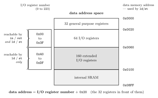
Figure 37: The bottom of the ATmega324A data address space, and the two numbering systems that live on it. Every I/O register has two numbers — its I/O register number (what in/out take) and its data memory address (what ld/st take) — and they differ by a constant 0x20, because the 32 general purpose registers sit in front of them in the same space. Only the first 64 I/O registers have an I/O register number small enough to fit the six operand bits of in/out; the 160 extended ones can be reached by their data address alone. The map follows the convention of csse2010-diagram-notation: lowest address at the top, hex addresses outside.
Extract from the I/O register list
The general purpose port registers are the first twelve entries, in the order PIN, DDR, PORT for each port in turn:
| Data address | I/O reg number | Name |
|---|---|---|
0x2B |
0x0B |
PORTD |
0x2A |
0x0A |
DDRD |
0x29 |
0x09 |
PIND |
0x28 |
0x08 |
PORTC |
0x27 |
0x07 |
DDRC |
0x26 |
0x06 |
PINC |
0x25 |
0x05 |
PORTB |
0x24 |
0x04 |
DDRB |
0x23 |
0x03 |
PINB |
0x22 |
0x02 |
PORTA |
0x21 |
0x01 |
DDRA |
0x20 |
0x00 |
PINA |
Further up the same list, to show the pattern continues and that reserved entries are real:
| Data address | I/O reg number | Name |
|---|---|---|
0x38 |
0x18 |
TIFR3 |
0x37 |
0x17 |
TIFR2 |
0x36 |
0x16 |
TIFR1 |
0x35 |
0x15 |
TIFR0 |
0x34 |
0x14 |
Reserved |
Read the two columns carefully in an exam question. out 0x02, r16 writes PORTA, but sts 0x02, r16 writes general purpose register r2 — the same number, two address spaces, and only the instruction tells them apart.
GPIO ports
The ATmega324A has four 8-bit general purpose I/O ports — PORT A, PORT B, PORT C, PORT D — appearing on the datasheet block diagram as PA7..0, PB7..0, PD7..0 around the edge of the chip, with port C drawn as PC5..0 plus TOSC1/PC6 and TOSC2/PC7 broken out separately — those two pins double as the timer oscillator connections. They are still port C bits, and DDRC/PORTC/PINC still cover all eight.
Three registers are associated with each (x = A, B, C or D):
| Register | Name | What it holds |
|---|---|---|
| DDRx | Data Direction Register | which pins are outputs |
| PORTx | values to output | |
| PINx | values on the pins |
Each is 8 bits — one bit per pin. DDRA0, PORTA0 and PINA0 are the three bits belonging to pin PA0.
What one bit of a port looks like
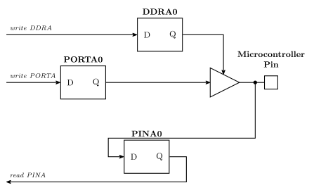
Figure 38: One bit of an AVR port — the three flip-flops behind pin PA0. DDRA0 enables the tri-state buffer, so it decides whether PORTA0’s value is driven onto the pin or the pin is left free for something outside to drive. PINA0 samples whatever is on the pin either way. Hence: DDR is direction, PORT is what you write, PIN is what you read.
1 means output, 0 means input. Writing 0xFF to DDRA makes every bit of port A an output, and writing 0x00 to DDRB makes every bit of port B an input.
Three consequences fall straight out of the circuit:
- PORTx does nothing on a pin whose DDRx bit is 0. The buffer is off; the value sits in the flip-flop unused. (On real AVR hardware it switches an internal pull-up instead.)
- PINx is always live. It samples the pin whether the pin is being driven from inside or outside, so reading PINx on an output pin reads back what you are driving.
- Reading PORTx is not reading the pin. It gives you the value you last wrote. To find out what is there, read PINx — which is why every input example uses
in rd, PINxand neverin rd, PORTx.
in and out
The two instructions that reach the first 64 I/O registers:
| Does | Operands | |
|---|---|---|
in rd, P |
Load I/O register value into general purpose register | rd: r0 to r31. P = I/O register number (0 to 63, 0x00 to 0x3F) or name |
out P, rr |
Store value from general purpose register into I/O register | rr: r0 to r31. P = 0 to 63 (0x00 to 0x3F) or name |
The operand order flips between them, and it flips for a consistent reason: like every AVR instruction, the destination is written first. So the I/O register is the second operand of in and the first of out.
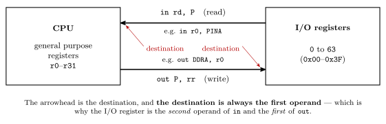
Figure 39: in and out between the two register files: the CPU’s general purpose registers r0–r31 and the first 64 I/O registers. in reads from an I/O register into a general purpose register, out writes the other way, and the head of each arrow, marked destination, is the operand written first. That is why the I/O register is the second operand of in and the first of out.
Answers of the form in DDRB, r16 are the standard trap. What is wrong with them is the mnemonic, not the direction: in’s destination is always one of r0–r31, so it can never be DDRB. Moving a general purpose register into an I/O register is exactly what out does — which is why the right answer in that shape is out DDRB, r16.
in and out reach all 32 general purpose registers, r0–r31 — unlike ldi, they are not restricted to the top half.
Both are one instruction word and one clock cycle, which makes them the cheapest way to touch a peripheral.
Three equivalences, all of them just the number/name table above:
| Written with a number | Same instruction, written with a name |
|---|---|
in r0, 0 |
in r0, PINA |
out 1, r0 |
out DDRA, r0 |
in r5, 0x26 |
in r5, TCNT0 — I/O register 0x26 is timer/counter 0 |
Using port names
Numbers are how the machine sees it; names are how you should write it:
.include "m324Adef.inc"The contents of this file are included directly in the program, and it defines the names for the I/O registers — so DDRA, PORTA, PINA, TCNT0 and the rest can be written instead of 0x01, 0x02, 0x00, 0x26. Everything about the generated machine code is identical; the assembler substitutes the number.
Setting port A (all bits) to be an output, which is the shape of nearly every initialisation block:
    ldi  r16, 0xFF       ; every bit 1 = output
    out  DDRA, r16       ; ... into the direction register
or, using the shorthand of avr-instructions, ser r16 in place of the ldi. Setting a port to be all inputs is the same two lines with 0x00 (or clr), and a mixed port is any other constant — DDRA is a bit pattern like everything else, so ldi r16, 0x0F gives four outputs and four inputs.
Changing one bit of a port
Writing a whole port register is right at initialisation. Afterwards a program usually wants to change one pin and leave the other seven alone, because the other pins belong to other parts of the program. In C that is a read-modify-write with a one-bit mask, the bit named rather than given as a number (bit-masking):
DDRC  |= (1<<5);          /* PC5 becomes an output     */
PORTC |= (1<<5);          /* PC5 driven high           */
PORTC &= ~(1<<5);         /* PC5 driven low            */
PORTC ^= (1<<5);          /* PC5 flipped               */
if (PINC & (1<<2)) { }    /* is PC2 high?              */
In assembly there are two ways:
| Register | Set or clear one bit | |
|---|---|---|
I/O registers 0 to 31, which includes every PINx, DDRx and PORTx |
sbi PORTC, 5 and cbi PORTC, 5 |
one instruction, other bits untouched |
any register in/out reach, 0 to 63 |
in r16, TCCR0B, then ori or andi with the mask, then out TCCR0B, r16 |
three instructions, and a spare register |
sbi and cbi hold the register number in five bits of the instruction, so they reach only the first 32 I/O registers. TCCR0B is I/O register 0x25, 37, which is past them: the long way is the only way. The extended registers past 63, such as TIMSK2 and TCCR1B, need lds and sts in place of in and out.
Writing to PINx
PINx is the port’s input register: reading it gives the levels on the pins. Writing to it is not storing a value. On the ATmega324A, writing a 1 to a bit of PINx toggles the matching bit of PORTx, whatever the pin’s direction, and writing a 0 does nothing.
That makes PINx a quick way to flip a pin:
PINC = (1<<0); /* toggle PC0; the 0s written to the other bits do nothing */and in assembly sbi PINC, 0 does the same in one instruction.
It also makes PINx the wrong register for a clear or a set. PINC &= ~(1<<5) does not clear PC5. If the compiler turns it into a single cbi PINC, 5, it writes a 0 to bit 5 of PINC and nothing happens. If it does a read, an AND and a write, it writes 1s to every other bit that read high, and those pins flip:
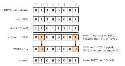
Figure 40: Why a read-modify-write on PINC goes wrong. Port C is all outputs, driving 0110 0001, so its pins read the same. PINC &= ~(1<<5) reads them, clears bit 5 of the reading and writes the result to PINC. A 1 written to a PINx bit is an order to toggle that bit of PORTx, not a value to keep, and a 0 does nothing. So the two other 1s, shaded, flip PC6 and PC0 low, and PC5, the bit meant to be cleared, stays high. The bottom row is what PORTC &= ~(1<<5) would have given.
So: set and clear through PORTx, read through PINx, and write PINx only to toggle.
Alternate pin functions
Most pins have a second job. When the peripheral that owns a pin is switched on, it takes the pin over from the port, and for some pins it overrides DDRx too. The serial interfaces use these:
| Port pin | Package pin | Alternate use | Peripheral |
|---|---|---|---|
| PB0 | 1 | XCK0 | USART0’s clock, used when it is an SPI master |
| PB4 | 5 | \(\overline{\text{SS}}\) | SPI (avr-spi) |
| PB5 | 6 | MOSI | SPI |
| PB6 | 7 | MISO | SPI |
| PB7 | 8 | SCK | SPI |
| PC0 | 22 | SCL | TWI |
| PC1 | 23 | SDA | TWI |
| PD0 | 14 | RXD0 | USART0 (avr-usart) |
| PD1 | 15 | TXD0 | USART0 |
| PD2 | 16 | RXD1 | USART1 |
| PD3 | 17 | TXD1 | USART1 |
| PD4 | 18 | XCK1 | USART1’s clock, used when it is an SPI master |
So the SPI port is the upper half of port B, and the TWI is the bottom two bits of port C. Other pins carry timer outputs, the external interrupts (INT0 and INT1 share PD2 and PD3 with USART1) and, on port A, the analog inputs. A pin can do only one job at a time, so a program that uses the SPI cannot also use PB4 to PB7 as general purpose I/O. The whole pinout is drawn in 2026-10-05-more-io.
Common mistakes
in DDRB, r16.inalways writes a general purpose register. Writing an I/O register isout DDRB, r16.- Reading
PORTxto find out what is on a pin. That gives back what was last written. The pins arePINx. - Setting or clearing a bit through
PINx. A 1 written there toggles, soPINC &= ~(1<<5)flips other pins and leaves PC5 alone. PORTC = (1<<5)to set one pin.=writes all eight bits and drives the other seven low. Use|=.sbiorcbion a register past 31, such asTCCR0B. They cannot reach it; usein,ori/andi,out.- Using a pin as general I/O while its peripheral is on. The SPI, the TWI and the USARTs take their pins over.
See also
- avr-architecture — the data address space these sit in, and the rest of the chip
- avr-instructions · avr-program-structure · bit-masking
- memory-models — why the I/O registers have two addresses
- io-board · device-pinouts — the switches, LEDs and buttons wired to the pins
- week6-lab-avr-io-ports — Lab 10, where this gets wired up
- avr-usart — PD0 and PD1 as a serial port · analog-to-digital-conversion — port A as analog inputs
- avr-spi — PB4 to PB7 as the SPI port · serial-communication — the TWI on PC0 and PC1
- 2026-08-31-instruction-set-architecture-part-1 — Lecture 11 · 2026-10-05-more-io — Lecture 19
AVR Assembly Program Structure
The skeleton every AVR assembly program in this course is built on — what goes at the top, where execution starts, and why it ends in an infinite loop. See avr-instructions for what fills it in and avr-io-ports for what the initialisation section usually does.
The template
                             ; Comments start with semicolons
.include "m324Adef.inc"

    jmp RESET                ; <- vector table
    ; Interrupt handlers go here
    ; (more on this in week 9/10)

RESET:                       ; Starting point   <- RESET handler
    ...                      ; Initialisation code
                             ; e.g. set DDRs

loop:                        ; <- main code
    ...                      ; Do stuff
    jmp loop                 ; Repeat
Three sections, and each is there for a reason:
| Section | What it is |
|---|---|
| Vector table | jmp RESET, then the interrupt handlers |
| RESET handler | the starting point — initialisation code, e.g. setting the data direction registers |
| Main code | the work, ending in a jump back to its own label |
Why the vector table comes first
The chip begins executing at program address 0x0000 — the top of the program memory map in memory-models — and the addresses immediately after it are reserved for interrupt vectors, one per interrupt source. So the very first instruction has to jump over them to reach the real start of the program. That is all jmp RESET is doing.
Everything between that jump and the RESET: label is the vector table itself. It stays empty (comments only) in a program that uses no interrupts — but the jmp has to be there from the first program, because without it execution would fall straight into whatever occupied the vector slots. Once a program does use an interrupt, each vector slot it needs holds a jmp to that source’s handler at a fixed address, placed with .org; the table, the handlers and how to enable them are in avr-interrupts.
Labels and jmp
A label is a name for a position in the program:
        jmp RESET
        …
RESET:  …
        …

loop:   …
        …
        jmp loop
The assembler replaces each label with the program-memory address it ended up at, so jmp loop becomes a jump to a real address. Two properties matter in practice:
- A label is written at the start of the line, ending in a colon; the instruction it names can be on the same line or the next one.
- Labels let you write code without ever computing an address by hand, which is most of what an assembler buys you over machine code (instruction-set-architecture).
jmp RESET at the top of the template needs the address of a label the assembler has not reached yet. It copes by reading the file twice: the first pass only works out where every label lands, using each line’s size, and the second fills the addresses into the instructions (assembly-process). In the template RESET is the address straight after the vector table, worked out the same way.
jmp itself is unconditional. For jumping only sometimes, the branch instructions below take a label in exactly the same way.
Conditional control flow
A branch instruction takes a label just as jmp does, but jumps only if a status register bit says so — so a decision is always written as two instructions, one that sets the flags and one that reads them:
breq label |
branch if Z = 1 |
brne label |
branch if Z = 0 |
The usual flag-setter is cp, which is a subtraction whose result is not saved: it computes rd - rr purely to set Z, N, C, V and the rest, so cp r5, r6 followed by breq branches exactly when the two registers were equal. The instruction reference specifies which status register bits are set by which instructions, per instruction rather than by one general rule — so a compare is not always needed, because whatever ran last may already have set Z. avr-instructions tabulates which does what.
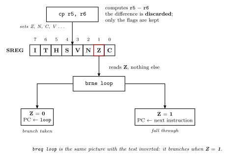
Figure 41: Compare-then-branch: the whole of an AVR conditional. cp performs the subtraction and throws the difference away, keeping only what it did to the flags; brne then reads exactly one of them and either loads the label’s address into the program counter or lets execution fall through to the next instruction. The flag names and their order are those of the AVR status register; the outline on Z marks the one flag brne tests.
Figure 41 is worth reading as the reason labels matter. The branch does not encode “go back three instructions” in a form you have to count out by hand; it names a label, and the assembler works out the address — the same service it performs for jmp RESET at the top of the file.
Two consequences for the template above. First, a loop that should sometimes end is still written as a label plus a branch, not as a special construct: the body falls through when the condition fails. Second, nothing may sit between the flag-setter and the branch that disturbs the flag being tested — the status register is a single shared piece of state, and the instruction in between will happily overwrite it.
The two branches above are the equality pair. The other eight — including the signed and unsigned less than pairs that a loop bound usually needs — and the loop idioms built from them are in avr-branches-and-jumps.
When the program calls procedures
The template above has no stack, because nothing in it calls anything. The moment a program uses call or rcall — or push — the stack pointer must be set first, and it goes at the top of RESET:, before any of the other initialisation:
RESET:
    ldi  r16, low(RAMEND)
    out  SPL, r16
    ldi  r16, high(RAMEND)
    out  SPH, r16
    ...                      ; then set DDRs and the rest as before
RAMEND is the last SRAM address, 0x08FF; the stack starts there and grows downward. Why it has to, and what call and ret do with it, is procedures-and-the-stack. A C program gets these four instructions for free from the compiler’s start-up code.
Variables and constants
The template holds only code. Variables and tables of constants go in the other segments (assembly-process), chosen by .dseg and .cseg:
.include "m324Adef.inc"
.def    temp = r16              ; a name for a register

        .dseg                   ; SRAM: space only
count:  .byte 1                 ; one byte, at 0x0100

        .cseg                   ; flash: code and constants
        jmp  RESET              ; vector table
RESET:
        ldi  temp, low(RAMEND)  ; stack pointer, if anything is called
        out  SPL, temp
        ldi  temp, high(RAMEND)
        out  SPH, temp
        ...                     ; initialisation
loop:
        ...                     ; main code
        jmp  loop

digits: .db  63, 6, 91, 79, 102, 109, 125, 7, 127, 111   ; seven-segment patterns, 0 to 9
Three rules come with it:
- A variable is a label on a
.bytein the data segment. It gets an address,0x0100for the first one, but no value. The program has to store something there, withsts count, tempfor example, before reading it. - Constants go in the code segment, out of the path of execution. The CPU runs whatever is in program memory at the PC, so a table in the middle of the code would be executed as if it were instructions. After the main loop’s
jmp loopis safe, because execution never gets there. Betweenjmp RESETandRESET:is safe for the same reason, but only in a program that uses no interrupts, because that is where the interrupt vectors go.digitsis ten bytes, an even number, so it fills five words with no pad (assembly-process). - A constant is read with
lpm, at its byte address, the label times 2, in Z (memory-models).
Why it ends in an infinite loop
loop: … jmp loop is not a placeholder. A microcontroller program has nowhere to return to — there is no operating system underneath it, and the CPU keeps fetching whatever comes next for as long as it has power. So the main body of an AVR program is a loop that never exits, and “do this repeatedly”, which is how nearly every lab task is worded, is the normal shape rather than a special case.
The division of labour that follows: anything that should happen once goes in the RESET handler (setting DDRs, loading constants), and anything that should happen forever goes in the loop (reading inputs, computing, writing outputs).
See also
- avr-branches-and-jumps — the full branch table, jumps, and the
if/loop idioms · procedures-and-the-stack —call,retand the stack - avr-interrupts — what goes in the vector table, and the handlers after it
- avr-instructions · avr-io-ports · avr-architecture
- assembly-process — statement fields, directives, segments and the two-pass assembler · instruction-set-architecture — assembly, the assembler and the toolchain
- memory-models — the program address space the vector table sits at the bottom of · memory-technologies — flash and SRAM, the memories behind
.csegand.dseg - week6-lab-avr-io-ports — Lab 10, where the template is first used
- 2026-10-08-assembly-process — Lecture 20: how the assembler turns the template into machine code
AVR Timers and Counters
The ATmega324A’s three timer/counter units: what they are, which pins and registers belong to each, how their clock is chosen and prescaled, the modes that decide what the count does when it reaches its top, the output compare actions that let a match drive a pin, and the one formula that turns a wanted event frequency into register values. From 2026-09-14-flow-of-control and 2026-09-17-pulse-width-modulation, with the register-level detail from week8-lab-avr-timers. PWM, the timers’ main use, has its own note: pulse-width-modulation.
Timer, counter
- A counter is a binary up/down counter clocked on some event.
- A timer is a counter clocked by a regular clock.
One piece of hardware, two names for what its clock is. Clock it from an external pin and each count is an event; clock it from the system clock and each count is a fixed slice of time, so the count is elapsed time. It is the wide, fast, silicon version of the counters of [counters], and it is separate hardware from the CPU: once configured it counts, compares and drives its pins with no instructions running, which is the whole reason to have it.
Three things a timer/counter is used for, in this course:
| Use | Clock | The event |
|---|---|---|
| Timing — do something every 100 ms, toggle an LED, tick a clock | system clock ÷ prescaler | the count reaching a compare value or wrapping, at a known interval |
| Counting — how many pulses arrived on a pin | edges on the external pin Tn |
the count reaching a compare value: that many pulses |
| PWM — an adjustable-width pulse on a pin, in hardware | system clock ÷ prescaler | the compare match switching the OCnx pin partway through each sweep |
The three units
| Timer/Counter 0 | Timer/Counter 1 | Timer/Counter 2 | |
|---|---|---|---|
| Width | 8-bit (0–255) | 16-bit (0–65535) | 8-bit (0–255) |
| Output compare pins | PB3 = OC0A, PB4 = OC0B |
PD5 = OC1A, PD4 = OC1B |
PD7 = OC2A, PD6 = OC2B |
| External clock pin | PB0 = T0 |
PB1 = T1 |
none — TOSC1/TOSC2 (PC6/PC7) take a separate crystal instead |
| Prescaler taps | 1, 8, 64, 256, 1024 | 1, 8, 64, 256, 1024 | 1, 8, 32, 64, 128, 256, 1024 |
| Modes | Normal, CTC, Fast PWM, Phase Correct PWM | Normal, CTC, Fast PWM, PC PWM, PFC PWM | Normal, CTC, Fast PWM, Phase Correct PWM |
| Count register | TCNT0 |
TCNT1H:TCNT1L |
TCNT2 |
| Control registers | TCCR0A, TCCR0B |
TCCR1A, TCCR1B, TCCR1C |
TCCR2A, TCCR2B |
| Compare registers | OCR0A, OCR0B |
OCR1AH:OCR1AL, OCR1BH:OCR1BL |
OCR2A, OCR2B |
| Interrupt registers | TIMSK0, TIFR0 |
TIMSK1, TIFR1 |
TIMSK2, TIFR2 |
Every unit has two compare units, A and B, each with its own register and its own pin. Timer 1 is the one to reach for when 255 is not enough: its 16 bits give periods 256 times longer at the same prescaler, and it is the timer Lab 12 sets up. Timer 2 is the one with a separate clock source, for real-time-clock use. The T/C 3 in the family datasheet’s block diagram is on the ATmega1284, not this chip (avr-architecture).
The pins are shared with GPIO. OC0A is PB3 until timer 0 is told to drive it; configuring a compare output takes the pin away from PORTB and hands it to the timer. The DDR bit must still be set to output, since the timer only decides what the pin shows, not whether it drives.
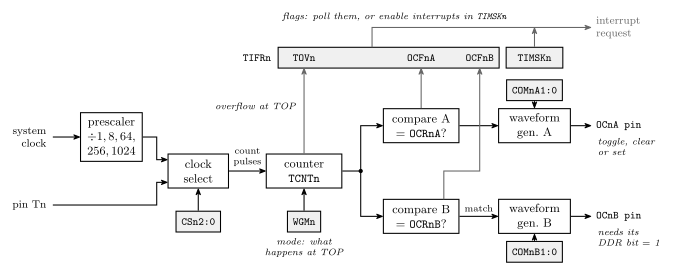
Figure 42: One timer/counter unit, from clock to pins. The clock select multiplexer feeds the counter either a prescaler tap or an edge on the external pin, or nothing; the counter increments on each pulse of whatever it is given. Two compare registers are each checked against the count every tick, and a match raises that unit’s flag and fires the waveform generator for its pin. Reaching the top of the count raises the overflow flag and, depending on the mode, wraps the count. The flags collect in TIFRn, where a program can poll them or, with the matching bits set in TIMSKn, have them raise an interrupt. Every box is configured through I/O registers and then runs with no CPU involvement.
Registers: data, control, interrupt
A timer is configured the way a port is — through I/O registers (avr-io-ports) — and its registers sort into the same three kinds:
| Timer registers | Port equivalent | ||
|---|---|---|---|
| data | TCNTn — the current count |
PIN / PORT |
read it to see where the count is; write it to preset |
| control | TCCRnA, TCCRnB (TCCR1C) — mode, clock, pin action; OCRnA, OCRnB — the values to match |
DDR |
set once, then leave |
| interrupt | TIMSKn — which events raise an interrupt; TIFRn — which events have happened |
— | read the flags by polling, or enable interrupts: avr-interrupts |
Where they are
The timer registers are spread across both the in/out range and the extended I/O space that only lds/sts reach (avr-io-ports):
| Register | I/O address | Data-memory address |
|---|---|---|
TCNT0 |
0x26 |
0x46 |
TCNT1L / TCNT1H |
— | 0x84 / 0x85 |
TCNT2 |
— | 0xB2 |
In C none of this matters: avr/io.h defines every one of them as a memory-mapped byte (c-preprocessor-and-avr-headers), and TCNT0, OCR1A and TCCR2B are assigned to like variables.
16-bit registers
Timer 1’s count and compare registers are two bytes each, and the hardware guards them with a shared temporary register so that a 16-bit value is read or written atomically: write the high byte first, then the low; read the low byte first, then the high. In assembly:
    ldi  r16, high(4321)
    sts  OCR1BH, r16       ; high byte first — goes into the temp register
    ldi  r16, low(4321)
    sts  OCR1BL, r16       ; low byte — both bytes land together
In C the compiler knows the rule, and OCR1B = 4321; is the whole thing. The H/L names still exist, but OCR1A, OCR1B, TCNT1 and ICR1 are 16-bit variables in the header.
The read rule has a consequence: reading TCNT1H on its own gives a stale value. Reading the low byte is what copies the high byte into the temporary register, and a read of the high byte returns that copy. So for the top half of the count, read the whole of TCNT1 and shift, as in TCNT1 >> 8, which reads the low byte first (below).
Choosing the clock
The count advances once per rising edge of whatever the clock select field CSn2:0 in TCCRnB picks — drawn as a multiplexer in 2026-09-14-flow-of-control:
CSn2 |
CSn1 |
CSn0 |
Timers 0 and 1 | Timer 2 |
|---|---|---|---|---|
| 0 | 0 | 0 | no clock — timer stopped | no clock |
| 0 | 0 | 1 | clk / 1 (no prescaling) | clk / 1 |
| 0 | 1 | 0 | clk / 8 | clk / 8 |
| 0 | 1 | 1 | clk / 64 | clk / 32 |
| 1 | 0 | 0 | clk / 256 | clk / 64 |
| 1 | 0 | 1 | clk / 1024 | clk / 128 |
| 1 | 1 | 0 | external pin Tn, falling edge |
clk / 256 |
| 1 | 1 | 1 | external pin Tn, rising edge |
clk / 1024 |
Two things to read off the table. A timer with CS = 000 does not run, which is both the reset state and the way to stop one. And timer 2’s codes are different — it spends the two external-pin codes on its extra prescaler taps — so a CS value copied from a timer-1 example means something else on timer 2.
The prescaler is a chain of dividers on the system clock (8 MHz on the lab boards), and each tap makes every count last that many system cycles. With an 8-bit timer the full 0-to-255 sweep therefore takes \(256 \cdot N\) cycles:
| Prescaler \(N\) | Tick | Sweep of 256 counts (8 MHz) | Sweep of 65536 counts (timer 1) |
|---|---|---|---|
| 1 | 0.125 µs | 32 µs | 8.2 ms |
| 8 | 1 µs | 256 µs | 65.5 ms |
| 64 | 8 µs | 2.05 ms | 524 ms |
| 256 | 32 µs | 8.19 ms | 2.1 s |
| 1024 | 128 µs | 32.8 ms | 8.4 s |
Coarse control over the period comes from this table; fine control comes from the compare registers and the mode.
Worked: a slow count from TCNT1 >> 8
With the clock divided by 1024, how quickly does TCNT1 >> 8 go up?
Timer 1 then counts \(8\ \text{MHz} / 1024 = 7812.5\) times a second. Shifting right by 8 drops the bottom eight bits, so what is left goes up by one every \(2^8 = 256\) counts:
\[\frac{7812.5}{256} = 30.5\ \text{Hz}, \quad\text{once every } 32.8\ \text{ms}.\]
TCNT1 >> 8 is the high byte of the count. It runs from 0 to 255 and comes back round to 0 every \(65\,536 / 7812.5 = 8.4\) seconds.
The same reasoning works for any shift. Each bit of a counter changes half as often as the bit below it, so TCNT1 >> k goes up \(7812.5 / 2^k\) times a second: 3906 for a shift of 1, 1953 for 2, and so on down to 30.5 for 8. A single bit is a square wave: (TCNT1 >> 12) & 1 changes every \(2^{12} = 4096\) counts, 0.52 s, which is enough to blink something about once a second without a single interrupt.
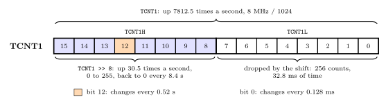
Figure 43: Timer 1’s count as a set of slower counters. With the clock divided by 1024 the whole of TCNT1 goes up 7812.5 times a second. Each bit changes half as often as the one to its right, so bit 8 changes once every 256 counts, and the top byte, TCNT1 >> 8, is a counter of its own that goes up 30.5 times a second and wraps every 8.4 s. Bit 12, shaded, changes every 0.52 s on its own.
In code, the timer only needs its prescaler, and it runs freely in normal mode:
TCCR1A = 0;
TCCR1B = (1<<CS12) | (1<<CS10);              /* normal mode, clock / 1024 */

uint8_t start = TCNT1 >> 8;
while ((uint8_t)((TCNT1 >> 8) - start) < 61) { }   /* 61 x 32.8 ms = 2.0 s */
The subtraction is done in 8 bits on purpose. When the count wraps from 255 to 0, now - start still comes out as the number of steps in between, so long as fewer than 256 have passed. week10-lab-adc-and-spi paces all its programs this way.
Modes: what happens at TOP
The waveform generation mode bits — WGM02:0 for the 8-bit timers, WGM13:0 for timer 1, split across TCCRnA and TCCRnB — decide what the count does when it reaches its TOP, and what TOP is:
| Mode | TOP | At TOP | Timer 0 WGM02:0 |
Timer 1 WGM13:0 |
|---|---|---|---|---|
| Normal | 0xFF / 0xFFFF | wrap to 0, set TOVn |
000 (0) |
0000 (0) |
| CTC — clear timer on compare match | OCRnA |
clear to 0, set OCFnA |
010 (2) |
0100 (4) |
| Fast PWM, fixed top | 0xFF | wrap to 0 | 011 (3) |
0101–0111 (8-, 9-, 10-bit) |
| Fast PWM, top in a register | OCRnA |
wrap to 0 | 111 (7) |
1111 (15; 1110 uses ICR1) |
| Phase correct PWM | 0xFF or OCRnA |
count back down | 001 (1), 101 (5) |
0001–0011, 1011 |
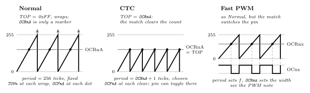
Figure 44: The three modes this course uses, as the count against time. In normal mode the counter runs to its full range and wraps; a compare value is just a marker it passes on the way, and the period is fixed at \(2^{8}\) or \(2^{16}\) ticks. In CTC mode reaching OCRnA clears the counter, so the compare value is the period and can be set to anything — the mode for producing an event at a chosen rate. In fast PWM the counter runs as in normal mode (or, in the register-top variant, as in CTC) while the compare match switches a pin partway through each sweep: the period sets the frequency and the compare value sets the pulse width. The same counter and the same compare registers produce all three; the mode bits only change what the top of the count means.
Normal is the mode after reset and the mode for a free-running count: read TCNTn to see how much time has passed, or let it overflow and take the overflow as the tick. CTC is the mode for an event every \(X\) ticks: the period is OCRnA + 1 exactly, with no wasted counts, and the count never exceeds the compare value. Both PWM modes are in pulse-width-modulation.
Output compare: what a match does to the pin
Each compare unit has two compare output mode bits, COMnx1:0 in TCCRnA, that decide what happens to the OCnx pin when TCNTn equals OCRnx. In the non-PWM modes (Normal, CTC):
COMnx1 |
COMnx0 |
On compare match |
|---|---|---|
| 0 | 0 | normal port operation — the pin belongs to the port, timer disconnected |
| 0 | 1 | toggle OCnx |
| 1 | 0 | clear OCnx — set the output low |
| 1 | 1 | set OCnx — set the output high |
Toggle is the useful one for a square wave: a CTC count that toggles the pin on every match produces a waveform whose frequency is half the match frequency, since it takes two matches for one full cycle. In the PWM modes the same bits select non-inverting (10) or inverting (11) output, and 01 becomes toggle OCnA on match only in the register-top mode — see pulse-width-modulation.
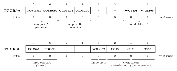
Figure 45: The two control registers of timer/counter 0, bit by bit, in the datasheet’s three-row form. The compare output mode fields sit at the top of TCCR0A, one two-bit field per compare unit; the three waveform generation mode bits are split, two at the bottom of TCCR0A and one in the middle of TCCR0B; the clock select field is the bottom three bits of TCCR0B. The two force-output-compare bits are for tests and are left alone. Every bit resets to 0, which decodes as normal mode, pins disconnected, timer stopped — so a timer does nothing until a program writes both registers. Timer 2’s registers have the same layout; timer 1 spreads the same fields over three registers with a fourth WGM bit.
Setting them from C uses the bit names from the header as shift counts, the idiom of bit-masking: TCCR1B = (1<<WGM12) | (1<<CS11) | (1<<CS10); selects CTC mode with clock ÷ 64 on timer 1, and TCCR0A = (1<<COM0A0); makes OC0A toggle on match. Write the whole register rather than |= when setting a timer up, so that nothing left over from before survives.
The master formula
Every timing question reduces to one relation between the clock, the prescaler and the top of the count:
\[f_{event} = \frac{f_{clk\_I/O}}{N \cdot (TOP + 1)}\]
- \(f_{clk\_I/O}\) is the device clock — 8 MHz on the ATmega324A boards.
- \(N\) is the prescaler: 1, 8, 64, 256 or 1024.
- \(TOP\) is the highest value the count reaches before it restarts: 255 or 65535 in normal mode and the fixed PWM modes, the value in
OCRnAin CTC mode and the register-top PWM modes. The \(+1\) is because the count from 0 to \(TOP\) takes \(TOP + 1\) ticks. - \(f_{event}\) is how often the count restarts — which is how often whatever is tied to the restart happens.
What the event is depends on what is hung off the timer:
| Tied to the restart | \(f_{event}\) is | Note |
|---|---|---|
| a pin set to toggle on match | the toggle rate | the resulting square wave has frequency \(f_{event}/2\) — one cycle needs a rise and a fall |
| a PWM output | the pulse rate | one falling edge per period in non-inverting mode, one rising edge in inverting |
| an interrupt | how often the handler runs | avr-interrupts |
Worked example. Toggle a pin 8 times a second (a 4 Hz square wave) from timer 1: \(f_{event} = 8\), so \(N \cdot (TOP + 1) = 8\,000\,000 / 8 = 1\,000\,000\):
| \(N\) | \(TOP + 1\) | \(TOP\) | Usable? |
|---|---|---|---|
| 1 | 1 000 000 | 999 999 | no — exceeds 65535 |
| 8 | 125 000 | 124 999 | no — exceeds 65535 |
| 64 | 15 625 | 15 624 | yes — integer and fits |
| 256 | 3 906.25 | — | no — not an integer |
| 1024 | 976.5625 | — | no — not an integer |
So OCR1A = 15624 in CTC mode with CS12:0 = 011. The recipe is always the same: fix \(f_{event}\), try each \(N\), keep the one that gives an integer \(TOP\) that fits the timer’s width; if none does exactly, take the nearest and accept the error. Lab 12 works this example in full (week8-lab-avr-timers).
Reading the flags
A program finds out that a match or overflow happened either by polling TIFRn, below, or by enabling the matching bit in TIMSKn so that the event raises an interrupt (avr-interrupts). When an interrupt is taken, the hardware clears the flag itself; a polling program must clear it. Two things about those flags are unlike anything on a port:
- A flag is cleared by writing a 1 to it, not a 0:
TIFR1 = (1<<OCF1A);clears the compare-A flag and leaves the others alone (writing 0 to a bit does nothing). It is the one place where|=is a mistake, since it would clear every flag that happened to be set. - The flag is set by the hardware whether or not the pin is connected or an interrupt is enabled, so a CTC timer with
COM = 00still raisesOCFnAevery period — a free periodic tick for a program that just needs to wait.
/* wait one period of a running CTC timer 1 */
while (!(TIFR1 & (1<<OCF1A))) { }   /* spin until the flag is set */
TIFR1 = (1<<OCF1A);                  /* clear it for next time */
See also
- pulse-width-modulation — the PWM modes, duty cycle and their formulas
- week8-lab-avr-timers — Lab 12:
TCCR1A/B/Cbit by bit, the master formula worked, two programs - week9-lab-avr-pwm — Lab 13: PWM on timers 0 and 1 · week9-lab-avr-interrupts — Lab 14: a 10 ms tick from timer 1
- week10-lab-adc-and-spi — Lab 16: a free-running timer 1 read as
TCNT1 >> 8to pace four programs - software-timers — one timer serving every timing job in a program
- avr-io-ports — I/O registers, the two address spaces,
in/outversuslds/sts - c-preprocessor-and-avr-headers — why
TCCR0AandOCR1Bcan be assigned to · bit-masking —(1<<CS11) - [counters] — the digital-logic counter this is built from · avr-architecture — the block diagram
- 2026-09-14-flow-of-control — Lecture 15 · 2026-09-17-pulse-width-modulation — Lecture 16
Bit Masking
Using a bitwise operation against a constant mask to touch only the bits you care about, leaving the rest alone. See boolean-algebra for the underlying laws and avr-instructions for the instructions used here. The same masks, written from the bit names in the AVR’s header files, are how every I/O register is set up in C: see set, clear and toggle and writing register bits by name.
Sometimes you are interested in only a few bits of a register. A bitwise AND can mask out the bits that are not of interest — and more generally, masking can selectively set, clear, toggle or extract bits.
The reason any of this is possible is that a bitwise instruction is not one eight-bit operation. It is eight independent one-bit operations running in parallel, and the two operands’ bit \(i\) decide result bit \(i\) with no reference to any other column.
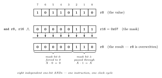
Figure 46: Why a mask works, one column at a time. Two rows of bits, an arrow down out of each column into a result row that overwrites the destination: here and r8, r16 with the mask 0x07, extracting the low three bits. The eight columns never interact — one mask bit decides one result bit, a 1 passing the value’s bit through and a 0 forcing it to zero — and all eight happen at once in a single instruction. Choosing a mask is therefore nothing more than deciding, position by position, which bits to keep.
Read Figure 46 column by column and the technique stops needing to be memorised: since the columns are independent, choosing a mask is just choosing, for each of the eight positions separately, whether that position gets passed through or forced.
The three identities that make it work
Each of AND, OR and XOR has a value that passes a bit through unchanged and a value that forces it. That pairing is the whole technique.
| \(X \cdot 0\) | \(X \cdot 1\) | \(X \cdot X\) | |
|---|---|---|---|
| AND | \(= 0\) | \(= X\) | \(= X\) |
| \(X + 0\) | \(X + 1\) | \(X + X\) | |
|---|---|---|---|
| OR | \(= X\) | \(= 1\) | \(= X\) |
| \(X \oplus 0\) | \(X \oplus 1\) | \(X \oplus X\) | |
|---|---|---|---|
| XOR | \(= X\) | \(= \overline{X}\) | \(= 0\) |
Reading off the pass-through and force columns gives the operation to reach for:
| To do this to the selected bits | Use | Mask bit = 1 on | Mask bit = 0 on |
|---|---|---|---|
| Clear them to 0 | AND |
the bits to keep — \(X \cdot 1 = X\) | the bits to clear — \(X \cdot 0 = 0\) |
| Set them to 1 | OR |
the bits to set — \(X + 1 = 1\) | everything else — \(X + 0 = X\) |
| Toggle them | EOR |
the bits to flip — \(X \oplus 1 = \overline{X}\) | everything else — \(X \oplus 0 = X\) |
| Extract them (others zeroed) | AND |
the bits to keep — \(X \cdot 1 = X\) | the bits to discard — \(X \cdot 0 = 0\) |
Note the asymmetry: AND’s mask is 1 on the bits you keep, whereas OR’s and XOR’s masks are 1 on the bits you act on. Getting that backwards is the usual bug — with AND you write the mask for what survives, with the other two for what changes.
\(X \oplus X = 0\) is the other one worth remembering: XORing a register with itself is the cheapest way to zero it.
In AVR assembly
The masks are ordinary constants, so the bitwise instructions of avr-instructions do the work. On AVR the immediate forms (andi, ori) only reach r16–r31; for a low register, load the mask into a high register and use the two-register form.
Extract the least significant three bits of r7 into r8, other bits of r8 zero.
    mov  r8, r7          ; copy the source
    ldi  r16, 0x07       ; mask 0000 0111 — keep the bottom three
    and  r8, r16         ; everything else forced to 0
Toggle the most significant four bits of r9, other bits unchanged.
    ldi  r16, 0xF0       ; 1111 0000 — flip the top four
    eor  r9, r16         ; bottom four XOR 0, so unchanged
Clear the least significant four bits of r10, other bits unchanged.
    ldi  r16, 0xF0       ; 1 on the bits to KEEP
    and  r10, r16        ; bottom four AND 0 -> 0
Set the most significant four bits of r11 to 1, other bits unchanged.
    ldi  r16, 0xF0       ; 1 on the bits to set
    or   r11, r16        ; bottom four OR 0, so unchanged
Note how 0xF0 appears as the mask in three of these with three different meanings — keep, flip, set — decided entirely by the instruction it is paired with.
In C
The same four operations with C’s bitwise operators (c-operators), which is how every AVR C program touches its ports. The masks are the same; the immediate-register restriction disappears, since the compiler chooses the registers.
| Operation | Operator | Example | Reads as |
|---|---|---|---|
| Clear particular bits | & with 0s on the bits to clear |
var = PINB & 0x0F; |
keep the low nibble, zero the high |
| Test particular bits | & with a 1 on the bit to test |
if (PINB & 0x02) … |
true if bit 1 is set |
| Set particular bits | \| with 1s on the bits to set |
PORTC = PINB \| 0x80; |
force bit 7 to 1 |
| Invert particular bits | ^ with 1s on the bits to flip |
PORTC = PINB ^ 0x0F; |
flip the low nibble |
Write the mask as a shift, not a hex constant: (1<<5) says bit 5 where 0x20 has to be decoded, and the header files name every register bit as a bit number for exactly this use (c-preprocessor-and-avr-headers):
DDRB  = (1<<5);                 /* bit 5 output, every other bit input: REPLACES the register */
DDRB |= (1<<4) | (1<<3);        /* bits 3 and 4 output, the rest unchanged: read-modify-write */
DDRB &= ~(1<<3);                /* bit 3 back to input, the rest unchanged                    */
PORTC ^= (1<<0);                /* toggle bit 0                                              */
TCCR1B = (1<<WGM12) | (1<<CS11) | (1<<CS10);   /* named bits, ORed into one value            */
The difference between the first two lines is the one that bites: = writes the whole register and silently sets the other seven bits to 0, |= ORs into what is already there. In assembly the second line is three instructions — in, ori, out — and the C compiler emits exactly those (week8-lab-avr-c-programming). For a single-bit clear the mask is the complement of the set mask, ~(1<<n), which is why clear bit 3 is &= ~(1<<3) and not &= (1<<3).
The test idiom needs no comparison. PINB & 0x02 is 0x02 when bit 1 is set and 0 when it is not, and C treats any non-zero value as true (c-control-flow) — so if (PINB & 0x02) is right and if ((PINB & 0x02) == 1) is always false, because the masked value is 2, never 1.
Set, clear and toggle on an I/O register
Changing one bit of an I/O register, and only that bit, is one of three lines. Each reads the register, combines it with a one-bit mask and writes it back:
| To | Write | The mask | Why the other bits survive |
|---|---|---|---|
| set bit n | REG \|= (1<<n); |
a 1 on bit n | \(X + 0 = X\) |
| clear bit n | REG &= ~(1<<n); |
a 0 on bit n, 1s elsewhere | \(X \cdot 1 = X\) |
| toggle bit n | REG ^= (1<<n); |
a 1 on bit n | \(X \oplus 0 = X\) |
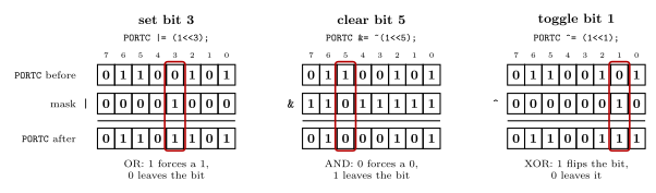
Figure 47: Set, clear and toggle on one register byte. Each panel starts from the same value of PORTC, 0110 0101, and changes one bit, outlined, with a single read-modify-write. The mask is a 1 shifted to the bit’s position, complemented for a clear. In every other column the mask holds the value that leaves a bit alone: 0 for OR and XOR, 1 for AND. Set gives 0110 1101, clear gives 0100 0101 and toggle gives 0110 0111, and each time the other seven bits are untouched.
Toggle is not enable. TIMSK2 ^= (1<<OCIE2A); turns the timer 2 compare A interrupt on only if it was off, and a second run turns it off again. To enable whatever the bit was before, set it with |=; to disable, clear it with &= ~. Toggling is for things meant to alternate, like an LED blinking.
The register has to be one that stores what is written. PORTx and DDRx do. PINx does not: it reads the pins, and on the ATmega324A a 1 written to one of its bits toggles the matching PORTx bit, so a read-modify-write on PINx changes the wrong bits (avr-io-ports).
Writing register bits by name
When setting or clearing bits of an I/O register, be explicit about which bits. Three ways to write the same value, from worst to best:
TCCR1B = 10;                          /* poor:   a number                    */
TCCR1B = 0x0A;                        /* better: the pattern, 0000 1010      */
TCCR1B = (1<<WGM12) | (1<<CS11);      /* best:   the bits, by name           */
WGM12 is bit 3 of TCCR1B and CS11 is bit 1, so all three are 0000 1010. Only the last says which bits, so a reader can check them against the datasheet without decoding anything: CTC mode, clock divided by 8 (avr-timers-and-counters). It costs nothing, either. The compiler works out (1<<WGM12) | (1<<CS11) while compiling, and all three lines become the same instructions.
The names are bit numbers. The device header that <avr/io.h> includes defines every bit name as the bit’s position in its register:
#define WGM02 3A name is not a mask; 1<< makes it one (c-preprocessor-and-avr-headers). The names are the datasheet’s, and the datasheet has errors in places, so the I/O register summary at the back is the one to check a name against.
Assembly uses the same names. In ldi r16, (1<<WGM02)|(1<<CS01) the assembler works out the constant, 0x0A, and the instruction stored is ldi r16, 0x0A.
A name belongs to one register. WGM12 and WGM02 are both 3, so (1<<WGM12) written into TCCR0B sets WGM02, and the compiler cannot notice, because all it sees is the number 3. Pair each name with the register whose datasheet entry defines it. The same byte 0x0A is CTC mode in TCCR1B and a reserved mode in TCCR0B (2026-10-05-more-io).
Masking sets the status flags too
Status register flags will be set also — a mask operation is a real ALU operation, not a free one. AND, OR and EOR all clear V and set N and Z from the result (C is untouched); see avr-architecture.
That side effect is often the actual point. andi r16, 0x01 keeps only bit 0, so:
\[Z = 1 \iff \text{bit 0 of } \texttt{r16} \text{ is } 0 \iff \texttt{r16} \text{ is even}\]
which makes a single masked AND an even/odd test. Any single-bit mask turns the Z flag into a test of that one bit — and tst rd, which is just and rd, rd, is the degenerate case that tests the whole register against zero.
Common mistakes
&= (1<<n)to clear bit n. That keeps bit n and clears the other seven. A clear’s mask is the complement,~(1<<n).=where|=was meant.DDRB = (1<<5)makes PB5 an output and every other pin of port B an input.- A bit name without the shift.
TCCR1B |= WGM12;ORs in the number 3,0000 0011, which setsCS11andCS10, clock divided by 64, and leavesWGM12alone. - A bit name in the wrong register.
(1<<WGM12)inTCCR0BsetsWGM02. ^=to enable. A toggle enables only from off; run twice, it disables.- A read-modify-write on
PINx. WritingPINxtoggles outputs, so it cannot clear or set a bit. - Getting AND’s mask backwards. With AND the 1s mark the bits to keep; with OR and XOR they mark the bits to change.
if ((x & mask) == 1). The masked value is the mask’s own value, so the test is false unless the mask is bit 0. Test for non-zero.
See also
- boolean-algebra · avr-instructions · avr-architecture
- avr-io-ports — one bit of a port in C and assembly, and why
PINxis different - avr-timers-and-counters — the
TCCRnBfields named in the examples - 2026-10-05-more-io — Lecture 19: poor, better and best,
TIMSK2toggled - week5-lab-avr-assembly-one — Lab 9, where these snippets are the exercise
- week8-lab-avr-c-programming — Lab 11, the same operations in C · c-operators · c-preprocessor-and-avr-headers
C Control Flow
The three shapes a C program’s control can take — sequential, selection and repetition — with the statements the course uses for each: if … else, while and for. First met in 2026-09-07-introduction-to-embedded-c-programming and 2026-09-10-more-c-programming-on-the-avr; the assembly equivalents are in avr-program-structure.
The three shapes
| Shape | Statements | |
|---|---|---|
| sequential | statements run one after another | the default — any list of statements |
| selection (decision) | a test picks one of two paths | if … else |
| repetition | a body runs again while a test holds | for, while |
All three are drawn as flowcharts in 2026-09-07-introduction-to-embedded-c-programming. Every program is built from nothing but these, nested.
Truth
There is no boolean type. C interprets any 0 value as false, anything else as true. So:
| Written | Means |
|---|---|
if(a) |
if(a != 0) |
if(!a) |
if(a == 0) |
Comparisons yield 1 or 0, so if (a > b) and if ((a > b) != 0) are the same test. A bitwise test like PINC & 0x01 yields either 0x01 or 0x00, which is why it can sit directly inside an if — anything non-zero is true, and it does not need to be exactly 1.
To the hardware a truth test is a compare against zero and a branch on Z — tst/cp then breq/brne in avr-instructions. if(a) is the C spelling of branch if not zero.
Selection — if
if (expression)
    stmt
else
stmt- The
elseclause is optional. stmtcan be replaced by multiple statements enclosed in braces{ }. Without the braces, only the one statement following theif(orelse) is conditional — a second line at the same indentation runs unconditionally, whatever the indentation suggests. Always use the braces.
An if used as a guard:
if(digit < 10) {
    PORTA = seven_seg[digit];
} else {
    PORTA = 0;
}
Four input bits can hold 0–15, the array has ten entries, and the if is what keeps seven_seg[digit] inside it (c-pointers-and-arrays — C does not check).
An else if chain is an else whose single statement is another if; nothing new is needed for it.
Repetition — while
while (expression)
    stmt
Test first; if true, run the body, then test again; stop when the test is false. If the test is false to begin with, the body never runs.
while(1) — a condition that is always true — is the shape of every embedded program:
int main(void) {
    /* set-up, once */
    DDRA = 0xFF;
    while(1) {
        /* read inputs, compute, write outputs — forever */
        digit = PINC & 0x0F;
        …
    }
}
On the AVR main has nowhere to return to. The program is set-up, then loop forever, and the loop body is one pass of reading inputs and writing outputs. In assembly this was a label and an unconditional rjmp back to it (avr-program-structure); while(1) is the same jump with the label hidden.
Repetition — for
for (init; test; step)
    stmt
is exactly
init;
while (test) {
    stmt
    step;
}
— the for only gathers the three parts of a counted loop onto one line so they cannot drift apart. Two traversals of the array a:
for(index=0; index<10; index++) {     /* init: index=0; test: index<10; step: index++ */
    a[index] = 0;
}

for(ptr=a; ptr < a+10; ptr++) {       /* same loop, counting in addresses */
    *ptr = 0;
}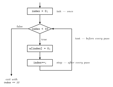
Figure 48: Where the three clauses of a for run, drawn on the repetition shape. init runs once, before anything; test runs before every pass, including the first; step runs after every pass, before the next test. The body of for(index=0; index<10; index++) therefore runs exactly ten times, with index taking 0 through 9 — and when the loop exits index is 10, the first value that failed the test. This is the while equivalence above, drawn.
The bound is the thing to get right. index < 10 runs the body for 0 through 9, the ten legal indices of a[10]; index <= 10 runs it once more, for a[10], which does not exist. The pointer form has the same edge: ptr < a+10 stops at the address one past the end without ever touching it.
Infinite loops, deliberately
The macro #define EVER ;; makes for(EVER) a spelling of for(;;) — a for with no init, no test and no step, which loops forever (c-preprocessor-and-avr-headers). It is while(1) in a different costume; the course’s programs use while(1).
Other control statements
switch, do … while, break and continue are all real C. They are not in these notes yet.
See also
- c-language-basics · c-operators · c-pointers-and-arrays · c-preprocessor-and-avr-headers
- avr-program-structure — labels and branches, the same shapes in assembly
- avr-instructions —
cp,breq,brne: what a test compiles to - 2026-09-07-introduction-to-embedded-c-programming — Lecture 13 · 2026-09-10-more-c-programming-on-the-avr — Lecture 14
C Operators
The operators the course uses, in groups — arithmetic, comparison, bitwise, logical, assignment — with the two families that look alike and are not, the shift operators and what they compile to, and the prefix/postfix rule. First met in 2026-09-07-introduction-to-embedded-c-programming; the signed/unsigned shift rule is in 2026-09-10-more-c-programming-on-the-avr. Types are in c-language-basics.
Binary operators
| Group | Operator | Meaning | AVR instruction behind it |
|---|---|---|---|
| arithmetic | + |
addition | add, adc |
- |
subtraction | sub, sbc |
|
* |
multiplication | mul |
|
/ |
division (integer, truncates toward 0) | a library routine — the AVR has no divide | |
% |
remainder (integer) | likewise | |
| comparison | > >= < <= |
ordering | cp then a branch on the flags |
== |
equal | cp then breq |
|
!= |
not equal | cp then brne |
|
| bitwise | & |
bitwise AND | and, andi |
\| |
bitwise OR | or, ori |
|
^ |
bitwise XOR | eor |
|
| logical | && |
logical AND | compare-and-branch sequences |
\|\| |
logical OR | ||
| assignment | = |
assignment | a mov, ld/st, or in/out — whatever the two sides are |
The instructions in the last column are in avr-instructions.
A comparison produces a value: 1 if true, 0 if false. So a > b is an ordinary expression that can be assigned, and (a > b) + (c > d) counts how many are true.
Unary operators
| Operator | Meaning | Example | AVR |
|---|---|---|---|
! |
logical not | !A ≡ Ā |
test-and-branch |
~ |
one’s complement (invert every bit) | ~A |
com |
- |
two’s complement (negate) | neg |
|
++ |
increment (prefix or postfix) | inc, or subi rd, -1 |
|
-- |
decrement (prefix or postfix) | dec |
Bitwise is not logical
The two pairs &/&& and |/||, and the pair ~/!, are the easiest mistake in C to make and the hardest to see.
- Bitwise
&,|,^,~work column by column: bit \(i\) of the result depends only on bit \(i\) of each operand. This is the eight-parallel-columns picture of bit-masking and theAND/OR/EOR/COMof avr-instructions. - Logical
&&,||,!treat each whole operand as true or false (non-zero or zero) and yield 1 or 0.
unsigned char a = 0x0F, b = 0xF0;

a & b      /* 0x00 — no column has a 1 in both  */
a && b     /* 1    — both are non-zero, so true */

~a         /* 0xF0 — every bit flipped           */
!a         /* 0    — a is non-zero, so "not a" is false */
a & b is zero and a && b is one, from the same two operands. Inside an if, if (PINC & 0x01) tests one bit, which is what is usually meant; if (PINC && 0x01) is true whenever anything on port C is high. The compiler accepts both.
== is not =
Read a = b as a ⇐ b.
=does.a = bcopiesbintoa. The arrow reading is the honest one: data flows right to left, the same destination first rule asmov rd, rrin avr-instructions.==asks.a == bis 1 if they are equal, 0 if not, and changes nothing.
if (a = 0) is legal C. It stores 0 in a, tests the stored value, and never takes the branch — silently.
Assignment shorthands
a += b is shorthand for a = a + b, and similarly -=, *=, /=, %=, &=, |=, ^=, <<=, >>=. a += 1 is the same as a++.
The three that matter most on the AVR are the bitwise ones, because they are the read-modify-write of a port in one line:
PORTA |= 0x01;      /* set bit 0, leave the rest    */
PORTA &= ~0x01;     /* clear bit 0, leave the rest  */
PORTA ^= 0x01;      /* toggle bit 0                 */
each a mask operation from bit-masking — and the ~ in the second is the reason the mask can be written as the bit to clear rather than as its complement.
Shifts
| AVR | ||
|---|---|---|
a << b |
a shifted left by b bits; 0 enters at the bottom |
lsl, b times |
a >> b |
a shifted right by b bits — logical if a is unsigned, arithmetic if a is signed |
lsr or asr, b times |
A left shift by \(n\) multiplies by \(2^n\); a right shift by \(n\) divides by \(2^n\), rounding toward \(-\infty\) for signed values. Two examples: 1 << 5 is \(1 \times 2^5 = 32\) and 3 << 4 is \(3 \times 2^4 = 48\) — worked in bits in the shift figure of 2026-09-07-introduction-to-embedded-c-programming.
The type picks the instruction. In assembly the programmer chose lsr or asr and thereby declared whether the byte was unsigned or signed (2026-09-03-instruction-set-architecture-part-2). In C there is one >>, and the declaration made the choice already:
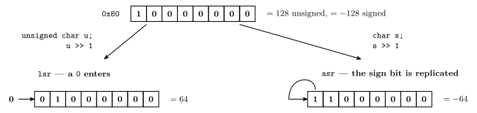
Figure 49: One operator, two instructions. The same bit pattern 10000000 is shifted right by one under two declarations. As unsigned char it means 128, the compiler emits lsr, a 0 enters at the top, and the result is 64. As char it means \(-128\), the compiler emits asr, the sign bit is copied back into the top, and the result is \(-64\). Both are the correct halving of what the bits were declared to mean.
1 << n is the mask with only bit \(n\) set. The AVR headers name every flag and pin as a bit number, so 1 << FLAG_NAME — with FLAG_NAME == 5 giving 00100000 — is how a mask is written from a name rather than a magic constant (c-preprocessor-and-avr-headers). Combined with the shorthands above:
PORTA |= (1 << 5);     /* set bit 5     */
PORTA &= ~(1 << 5);    /* clear bit 5   */
if (PINC & (1 << 3))   /* test bit 3    */
Prefix and postfix ++ and --
a++ and ++a both add one to a. They differ in what the expression is worth:
| Order | Rule | |
|---|---|---|
postfix a++ |
use value, change value | the expression is the old a; then a becomes a + 1 |
prefix ++a |
change value, use value | a becomes a + 1; the expression is the new a |
Every use is two statements in disguise, and only the order differs:
int a,b,c,d,e;
a = 4;
b = a++;    /* b=a;   a=a+1; */   /* b=4, a=5 */
c = --a;    /* a=a-1; c=a;   */   /* a=4, c=4 */
d = ++a;    /* a=a+1; d=a;   */   /* a=5, d=5 */
e = a--;    /* e=a;   a=a-1; */   /* e=5, a=4 */
Final values: a=4, b=4, c=4, d=5, e=5.
Worked: a = 1; b = 3; b += a++; leaves b = 4, because b += a++ is b = b + a with the old a, and only then a = a + 1. An answer of 5 applies the increment first, which is what ++a does.
On its own line, a++; and ++a; are indistinguishable: the value of the expression is thrown away, and only the change remains. The difference exists only when the expression is used — assigned, passed, indexed, as in values[9] = values[8]++; (c-pointers-and-arrays).
Precedence
The one place precedence bites is the SQUARE(1+2) example in c-preprocessor-and-avr-headers, where * binding tighter than + turns (1+2*1+2) into 5. The rule the course relies on is the schoolroom one — *, /, % before +, - — and the practical advice is parenthesise anything you would have to think about. Two cases to know because the natural reading is wrong:
&binds looser than==, sox & 1 == 0isx & (1 == 0), i.e.x & 0. Write(x & 1) == 0.<<binds looser than+, so1 << n + 1is1 << (n + 1). Write(1 << n) + 1if that is what is meant.
These are the two that catch AVR code in particular.
See also
- c-language-basics · c-control-flow · c-pointers-and-arrays · c-preprocessor-and-avr-headers
- bit-masking — the set/clear/toggle/extract patterns the bitwise operators write
- avr-instructions — the instructions each operator compiles to, including
lsl/lsr/asr - boolean-algebra — the laws behind
&,|,^and~ - floating-point-numbers — integer
/against floating point on the AVR:PINA / 3andPINA * 0.334f - 2026-09-07-introduction-to-embedded-c-programming — Lecture 13 · 2026-09-10-more-c-programming-on-the-avr — Lecture 14
C Pointers and Arrays
Arrays, pointers, and the fact that connects them: an array name is the address of its first element, and pointer arithmetic counts in elements, not cells. Both are made concrete in the AVR’s 8-bit data memory (memory-models), where an int is two cells and so a + 5 is ten cells past a. First met in 2026-09-10-more-c-programming-on-the-avr; the language basics are in c-language-basics.
Arrays
Declaring: type variable_name[size];
char message[16];
int  values[10];
uint8_t seven_seg[10] = { 63,6,91,79,102,109,125,7,127,111 };   /* with initial values */
Accessing: variable_name[index], with index = 0 … size−1 — zero-based indexing. A 365-element array has elements [0] through [364]; [365] is not one of them.
message[0] = 'c';
values[9] = values[8]++;        /* copies the OLD values[8], then increments it */
The declaration reserves size elements of the type contiguously — one after another with nothing between — which is what makes both the indexing and the pointer arithmetic below work. The elements are ordinary variables of the element type; values[3] is an int like any other.
C does not check the index. values[10] and values[-1] compile, and at run time they read or write whichever cell happens to sit past the end or before the start. The seven_seg[digit] lookup is guarded with if(digit < 10) for exactly this reason (c-control-flow).
Pointers
A pointer variable stores a memory address. Declaration: type *variable_name; — variable_name is a pointer to something of the given type.
char a, b;
char *ptr;          /* or all on one line: char a,b,*ptr; */

ptr = &a;           /* & — address-of: ptr now holds a's address  */
b = *ptr;           /* * — indirection: the value at that address */
The two operators are inverses:
| From | To | ||
|---|---|---|---|
&a |
a variable | its address | address-of — makes a pointer |
*ptr |
an address | the value stored there | indirection — follows a pointer |
In memory, say a holds 8 at address 400, b is at 434, and ptr is at 576 holding 400 — an address, not a value (drawn in 2026-09-10-more-c-programming-on-the-avr). ptr is a variable like the others, with its own cell; only its contents are special. On the AVR a data address is 16 bits (memory-models), so a pointer is two cells whatever it points at.
*ptr can also be assigned to: *ptr = 0; writes through the pointer into whatever it points at. That is how the pointer traversal below clears an array.
The * in a declaration and the * in an expression are different things. char *ptr; declares ptr as a pointer; *ptr later uses it. The declaration form reads as the thing *ptr is a char.
The hardware view
A pointer is the indirect addressing mode of addressing-modes as a language feature. ptr plays the part of the X, Y or Z register pair, *ptr is ld rd, X, and *ptr = v is st X, rr. ptr++ is the post-increment form ld rd, X+ that the instruction set provides precisely because walking a table is so common. The compiler chooses which of X, Y, Z it uses.
Arrays are pointers to their first element
An array name can be treated as a pointer to the first element — the address of the first element.
int a[10];
int *ptr;

/* the following are the same */
ptr = a;
ptr = &a[0];
So a on its own is an address, a[0] is the int there, and *a is the same int. In general a[i] is *(a + i) — the bracket notation is shorthand for pointer arithmetic, which is why the arithmetic has the rule it has.
Pointer arithmetic
Addition and subtraction on pointers work in multiples of the size of the object pointed to.
int a[10];
int *ptr;

/* the following are the same */
ptr = a+5;
ptr = &a[5];
If a starts at 300 and an int is 16 bits — two 8-bit cells — then a + 5 is 310, not 305: five elements on, two cells each. The sum is 300 + 2·5 = 310, not 300 + 5 = 305. The array is drawn in memory in 2026-09-10-more-c-programming-on-the-avr.
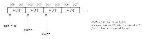
Figure 50: ptr++ on a pointer to int, on the AVR. Each step moves the pointer by one element, which is two 8-bit cells, so the addresses it visits are 300, 302, 304, … and it lands on every element exactly once. The same ptr++ on a char pointer would step by one cell. The compiler multiplies the step by the element size; the source says ++ either way. The pointer is the traversal loop’s, drawn at three successive steps.
The consequences:
- The same expression means different addresses for different types.
a + 5is 310 forint a[]and 305 forchar a[]. The type is part of the arithmetic. ptr - acounts elements, not cells: forptr = &a[5]it is 5.- Comparison works in addresses.
ptr < a + 10is true whileptris inside the array. intis 16 bits on the AVR; on a 32-bit machinea + 5would be twenty cells on. The rule is stated in terms of the size of the object because the number is machine-dependent (c-language-basics).
Traversing an array
Two ways to clear int a[10]:
/* using an index */
int a[10];
int index;
for(index=0; index<10; index++) {
    a[index] = 0;
}

/* using a pointer */
int a[10], *ptr;
for(ptr=a; ptr < a+10; ptr++) {
    *ptr = 0;
}
Adding one to an array pointer makes it point to the next element in the array. The two loops visit the same ten cells in the same order. The index loop computes a + index afresh each pass; the pointer loop keeps that address in ptr and steps it. The bound is the same in both — the address one past the last element, tested with < so it is never touched. See c-control-flow for the for itself.
The pointer form is closer to what the compiler emits either way — a register pair holding an address, an st X+, r in the body — which is why C has it.
Strings, briefly
A string constant "abc" (c-language-basics) is an array of char with a terminating zero byte after the last character, so "abc" occupies four cells. char message[16]; therefore holds at most fifteen characters, though message[16] looks like room for sixteen. The terminator is standard C.
See also
- c-language-basics · c-operators · c-control-flow · c-preprocessor-and-avr-headers
- memory-models — 8-bit data cells, 16-bit addresses, alignment
- addressing-modes — indirect addressing, which a pointer is
- avr-instructions —
ld/stwith X, Y, Z and their post-increment forms - seven-segment-display — the
seven_seg[10]lookup table - 2026-09-10-more-c-programming-on-the-avr — Lecture 14
C Preprocessor and AVR Headers
The preprocessor — #include and #define — and the three lines of avr/io.h that let DDRA = 0xFF; be written as if a hardware register were a variable. First met in 2026-09-10-more-c-programming-on-the-avr; the port registers themselves are in avr-io-ports.
What the preprocessor is
C programs are first parsed by a preprocessor, which replaces preprocessor directives with substitute text. Only then does the compiler see the program. Directives start with #:
| Directive | Does |
|---|---|
#include … |
paste in a file |
#define … |
define a macro — a textual substitution |
#if, #ifdef, #else, #undef, … |
conditional inclusion, un-definition, and others |
The preprocessor does not know C. It edits text. Whatever it produces is what the compiler compiles, and every surprise in this note comes from forgetting that.
#include
| Form | Kind of header | Looks in |
|---|---|---|
#include <filename.h> |
system | the system include directories — where avr/io.h and stdio.h live |
#include "filename.h" |
user-defined | your own project directory first |
The directive is replaced by the whole contents of the named file, at that point. After preprocessing there is one file, with the header pasted in at the top.
Header files
Header (.h) files are used for common macros, function prototypes etc — the C counterpart of m324Adef.inc in assembly (avr-io-ports).
stdio.h— prototypes ofprintf()etc. The AVR has a simplified version (no files);printf()only works if you say where the characters go, e.g. a serial port.avr/io.h— defines the AVR’s useful constants and functions/macros. Definitions depend on the actual device targeted: it reads which chip is being compiled for and pulls in that chip’s register map, soDDRAmeans the right address for the ATmega324A and a different one for another part. It also suppliesuint8_tand the other fixed-width types.
Every program in the course starts with #include <avr/io.h>.
Headers against libraries
A header file is not the library. A header
- defines useful preprocessor macros,
- declares the functions that are in the library, as function prototypes, and
- declares variables that are available externally, with
extern.
The library is the collection of object files that implements the functions (compilation-and-linking).
A prototype such as int printf(const char *fmt, ...); tells the compiler the name, the argument types and the return type. That is enough for the compiler to check a call and generate it. There is no code in it, so in main.o the call to printf is left as an external reference. The code is in the library, an object file printf.o inside it, and the linker joins it on and fills in the address. An extern declaration does the same for a variable: extern int count; says that count exists somewhere else and reserves nothing.
So the header goes to the compiler, through the preprocessor, and the library goes to the linker. The two kinds of mistake show up at different steps:
| Missing | Shows up when | Typical message |
|---|---|---|
the #include |
compiling | implicit declaration of function printf |
the library, or the .c file that defines the function |
linking | undefined reference to printf |
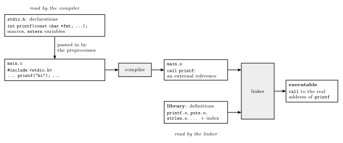
Figure 51: Where a header and a library each come into play, for a program that calls printf. The header holds only declarations. The preprocessor pastes it into main.c so that the compiler can check and generate the call, and in main.o that call is still an external reference. The library holds the definitions, as already compiled object files with an index. The linker finds printf.o through the index, links it in, and fills in the call. The header is used by the compiler and the library by the linker.
#define — macros
Macros are textual substitutions.
| Macro | Effect |
|---|---|
#define pi 3.1415 |
every later pi becomes 3.1415 — A = pi * r²; becomes A = 3.1415 * r²; (the superscript is shorthand; in real C the square would be r * r) |
#define EVER ;; |
for(EVER) becomes for(;;), an infinite loop |
#define sum(a,b) (a+b) |
a macro with parameters: sum(x, 2) becomes (x+2) |
A macro with parameters looks like a function call and is not one: no call happens, the arguments are pasted into the body as text, and the result is compiled in place.
The SQUARE trap
Given
#define SQUARE(x) (x*x), what isSQUARE(1+2)?
5, not 9. Paste the text: (1+2*1+2). Multiplication binds tighter than addition, so it is \(1 + 2 + 2\). The argument was never evaluated first, because there is no function to evaluate it.
The fix is parentheses around every parameter, and around the whole body:
#define SQUARE(x) ((x)*(x)) /* SQUARE(1+2) -> ((1+2)*(1+2)) = 9 */The outer pair matters as much as the inner: without it, 1 / SQUARE(a) becomes 1 / (a)*(a), which is \(a\), not \(1/a^2\). Write every macro this way. The AVR headers below do — note the brackets around (mem_addr) and (io_addr).
A second pitfall: an argument with a side effect is pasted as many times as the parameter appears. SQUARE(i++) becomes ((i++)*(i++)) and increments i twice.
The avr/io.h register macros
The definitions behind the port names, from avr/io.h and the device header it includes:
#define _MMIO_BYTE(mem_addr) \
                (*(volatile uint8_t *)(mem_addr))
#define _SFR_IO8(io_addr) \
                _MMIO_BYTE((io_addr) + 0x20)

/* Input Pins, Port A */
#define PINA      _SFR_IO8(0x00)

/* Data Direction Register, Port A */
#define DDRA      _SFR_IO8(0x01)

/* Data Register, Port A */
#define PORTA _SFR_IO8(0x02)(\ at the end of a line continues a directive onto the next line.)
Upshot: I/O register names can be used as variables.
DDRA = 0xFF;
PORTA = PINC | 0xF0;
Unrolling DDRA
| Step | Text |
|---|---|
| as written | DDRA = 0xFF; |
#define DDRA |
_SFR_IO8(0x01) = 0xFF; |
#define _SFR_IO8 |
_MMIO_BYTE((0x01) + 0x20) = 0xFF; |
#define _MMIO_BYTE |
(*(volatile uint8_t *)((0x01) + 0x20)) = 0xFF; |
Reading the final line from the inside out:
(0x01) + 0x20is0x21— a number.(volatile uint8_t *)casts it: treat this number as the address of an 8-bit unsigned byte. Now it is a pointer (c-pointers-and-arrays).- The leading
*dereferences it: the byte at that address. = 0xFFstores into that byte.
So DDRA = 0xFF; is a store to data address 0x21, and x = PINC; is a load from data address 0x26. There is no variable called DDRA anywhere; the name dissolves before the compiler sees it.
Why + 0x20
The AVR’s 64 I/O registers have two addresses each (avr-io-ports): an I/O-space number 0–63, which is what in and out use, and a data-space address 0x20 higher, where lds/sts — and any C pointer — find the same register. DDRA is I/O 0x01 and data 0x21. The macro takes the I/O number the datasheet lists and adds the offset, because a C pointer can only name data-space addresses. (The compiler, seeing a constant address in the I/O range, will usually emit in/out anyway.)
Why volatile
volatile tells the compiler the value at this address can change without the program changing it, and that every read and write matters. Without it the compiler is entitled to assume that a byte it wrote a moment ago still holds what it wrote, and that two reads with nothing between them give the same answer — both false for a port: PINC changes whenever the pins do, and PORTA is written for its effect on the pins, not to be read back. volatile forbids the optimisations that would break that. It is the one piece of the macro that is about hardware rather than addressing.
The same keyword belongs on any ordinary variable that an interrupt handler writes. To the code in main, a handler’s write is as invisible as a pin changing, and for the same reason: nothing in main’s own flow of control explains it. See avr-interrupts.
Naming bits
The headers also define bit numbers for every flag and pin — for example FLAG_NAME == 5 — so a mask is written from a name rather than a constant:
1 << FLAG_NAME              /* 00100000 when FLAG_NAME is 5 */
PORTA |= (1 << 5);          /* set one bit                   */
PORTA &= ~(1 << 5);         /* clear one bit                 */
The shift and the |=/&= shorthands are in c-operators; the mask patterns are in bit-masking. FLAG_NAME is a placeholder name; the actual names for the ATmega324A’s pins and flags come from the device header, as #define WGM02 3 does in 2026-10-05-more-io.
See also
- avr-io-ports — the port registers, and the I/O-space versus data-space address columns
- c-pointers-and-arrays — what
*(uint8_t *)addrmeans - c-operators —
1 << n,|=,&= - bit-masking · memory-models
- avr-interrupts —
volatileon variables shared with an interrupt handler - compilation-and-linking — what happens after the preprocessor: object files, libraries and the linker · 2026-10-15-compilation-and-linking — Lecture 22
- 2026-09-10-more-c-programming-on-the-avr — Lecture 14
Counters
A counter is a multi-bit register that goes through a determined sequence of states (values) upon the application of input (clock) pulses. It is a synchronous sequential circuit built from D flip-flops plus some combinational logic in the feedback path.
Binary counters
A counter which follows the binary number sequence is a binary counter.
An \(n\)-bit binary counter:
- has \(n\) flip-flops;
- has \(2^n\) different states;
- counts from \(0\) to \(2^n - 1\), then wraps back to \(0\).
For example, a 2-bit binary counter counts
\[00 \to 01 \to 10 \to 11 \to 00 \to \ldots\]
i.e. \(0 \to 1 \to 2 \to 3 \to 0 \to \ldots\)
4-bit binary counter — counting sequence
| Bit 3 | Bit 2 | Bit 1 | Bit 0 | Value |
|---|---|---|---|---|
| 0 | 0 | 0 | 0 | 0 |
| 0 | 0 | 0 | 1 | 1 |
| 0 | 0 | 1 | 0 | 2 |
| 0 | 0 | 1 | 1 | 3 |
| 0 | 1 | 0 | 0 | 4 |
| 0 | 1 | 0 | 1 | 5 |
| 0 | 1 | 1 | 0 | 6 |
| 0 | 1 | 1 | 1 | 7 |
| 1 | 0 | 0 | 0 | 8 |
| 1 | 0 | 0 | 1 | 9 |
| 1 | 0 | 1 | 0 | 10 |
| 1 | 0 | 1 | 1 | 11 |
| 1 | 1 | 0 | 0 | 12 |
| 1 | 1 | 0 | 1 | 13 |
| 1 | 1 | 1 | 0 | 14 |
| 1 | 1 | 1 | 1 | 15 |
| 0 | 0 | 0 | 0 | 0 |
Each bit toggles at half the rate of the bit to its right — bit 0 changes every count, bit 1 every second count, bit 2 every fourth, bit 3 every eighth.
Key points
- The next state is a function of the present state (and possibly of external inputs).
- The count sequence can be the binary numbers but does not have to be — if it is, the counter is a binary counter; otherwise it is just some arbitrary cycle through states.
- These circuits are synchronous: all flip-flops share the same clock.
- Asynchronous counters exist too, but are not discussed in this course.
State: the design idea
This is the whole trick, and it is what makes counter design mechanical:
- The values stored in the flip-flops are the current (present) state of the circuit.
- The \(D\) inputs to the flip-flops are the next state — whatever is sitting on \(D\) at the clock edge becomes the new state.
- The \(D\) inputs are some combinational function of the current state (and of any external inputs).
So for a counter with state bits \(Q_{n-1} \ldots Q_1 Q_0\), designing the counter means finding \(n\) Boolean expressions
\[D_i = f_i(Q_{n-1}, \ldots, Q_1, Q_0)\]
and building each one out of gates.
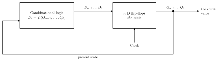
Figure 52: A counter is the general sequential-circuit block diagram with the external inputs deleted. That diagram, as Mano draws it, is a combinational circuit feeding flip-flops, the flip-flop outputs routed back round to the combinational circuit, and the clock entering the flip-flops on its own labelled stub. A counter may or may not have external inputs; removing them, as here, is what makes the design mechanical: with nothing else to depend on, each D is a function of the Q values alone, so the present-state/next-state table below is a complete specification of the circuit.
Design recipe
- Write down the count sequence you want, as a cycle of state values.
- Build a present-state / next-state table. One row per possible state — all \(2^n\) of them, not just the ones in your sequence. Columns: present state \(Q_{n-1}\ldots Q_0\), then next state \(D_{n-1}\ldots D_0\). Fill each next-state entry by reading off what follows that state in your sequence.
- Handle unused states. If your sequence doesn’t use all \(2^n\) states, the next state for the unused ones is a don’t-care (X). You may set each X to whatever makes the algebra simplest — but check afterwards where the unused state actually goes, because a self-correcting counter (one whose unused states lead back into the cycle) is nicer than one that can get stuck.
- Read each \(D\) column as a Boolean function of the \(Q\)s. The table is a truth table with the \(Q\)s as inputs and \(D_i\) as the output, so write it in sum-of-products form: OR together one AND term per row where \(D_i = 1\). See boolean-algebra.
- Simplify each expression using the Boolean algebra laws (and the don’t-cares), then draw the circuit: the combinational logic for \(D_i\) feeding flip-flop \(i\), with every flip-flop on a common clock. See circuit-schematics for schematic conventions and device-pinouts for the 74HCT74 / 74HCT175 D flip-flop packages.
The smallest case falls straight out of the recipe: a 1-bit counter counts \(0 \to 1 \to 0 \to \ldots\), so its next state is always the complement of its present state, giving \(D = \bar Q\) — a single flip-flop with its \(\bar Q\) output wired back to its own \(D\) input (a toggle).
Worked example — a 2-bit counter for \(00 \to 10 \to 01 \to 00\)
Step 1–2 — present-state / next-state table. The sequence uses three of the four states; \(11\) is unused, so its next state is a don’t-care.
| \(Q_1\) | \(Q_0\) | \(D_1\) | \(D_0\) | comment |
|---|---|---|---|---|
| 0 | 0 | 1 | 0 | \(00 \to 10\) |
| 0 | 1 | 0 | 0 | \(01 \to 00\) |
| 1 | 0 | 0 | 1 | \(10 \to 01\) |
| 1 | 1 | X | X | unused state |
Step 4 — read off the columns.
\(D_1\) is 1 only in the row \(Q_1Q_0 = 00\). Making the don’t-care 1 would give \(Q_1 \odot Q_0\) (XNOR), which is no simpler, so take the don’t-care as 0 (\(X_1 = 0\)):
\[D_1 = \bar Q_1 \bar Q_0\]
\(D_0\) is 1 only in the row \(Q_1Q_0 = 10\), which gives \(D_0 = Q_1\bar Q_0\). Here the don’t-care does help: setting it to 1 (\(X_0 = 1\)) makes \(D_0 = 1\) for both rows with \(Q_1 = 1\), so
\[D_0 = Q_1\]
Step 5 — the circuit. Two D flip-flops on a common clock. Flip-flop 0’s \(D\) input is wired directly to flip-flop 1’s \(Q_1\) output — no gate at all. Flip-flop 1’s \(D\) input is driven by a 2-input NOR of \(Q_1\) and \(Q_0\) (since \(\bar Q_1 \bar Q_0 = \overline{Q_1 + Q_0}\)), or equivalently by an AND of the two \(\bar Q\) outputs.
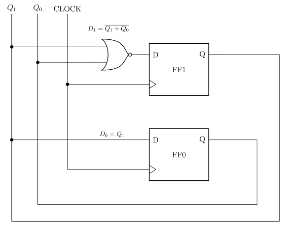
Figure 53: The whole counter, drawn from the derivation above. Each Q runs back to a vertical rail that the next-state logic taps, which is the physical form of the feedback loop in the block diagram earlier: D0 is FF1’s Q wired straight across with no gate at all, and D1 is one NOR gate. Dots are connections; where the Q0 rail and the CLOCK rail cross the D0 wire there is no dot and no connection. The circuit takes the NOR form of D1; an AND of the two Q-bar outputs is the same function and would need the flip-flops’ Q-bar pins instead.
Check, including the unused state:
| present | \(D_1 D_0\) | next |
|---|---|---|
| 00 | 1 0 | 10 |
| 10 | 0 1 | 01 |
| 01 | 0 0 | 00 |
| 11 | 0 1 | 01 |
The cycle is right, and the unused state falls into the cycle on the next clock edge, \(11 \to 01\), so the counter is self-correcting — a robust design. (Choosing \(D_0 = Q_1\bar Q_0\) instead — don’t-care set to 0 — would send \(11 \to 00\), also fine, at the cost of a whole extra gate: an AND fed from \(Q_1\) and the flip-flop’s \(\bar Q_0\) pin, where \(D_0 = Q_1\) needs no gate at all.)
Applied exercise
week4-lab-lab-7-exercises is exactly this recipe at \(n = 3\): design a 3-bit synchronous counter that steps through an allocated 7-state sequence, with the eighth (missing) state treated as a don’t-care.
Fetch-Decode-Execute Cycle
What the control unit actually does: a continuous cycle over the datapath, issuing control signals in the right order for whatever instruction it just read. See cpu-organisation for the blocks involved and arithmetic-logic-unit for the one being driven.
The cycle
The control unit operates in a continuous cycle on the datapath:
| Stage | What happens |
|---|---|
| Fetch | Fetch an instruction from memory and bring it inside the CPU. Two special purpose registers involved — PC and IR |
| Decode | Resolve the operation (opcode) and operands (variables) |
| Execute | Control signals are issued and the operation takes place in the datapath |
Stated as steps:
- Fetch the next instruction from memory into the Instruction Register (IR).
- Change the Program Counter (PC) to point to the next instruction.
- Determine the type of (decode) the instruction just fetched — i.e. look at the opcode.
- Execute the instruction.
- Return to step 1.
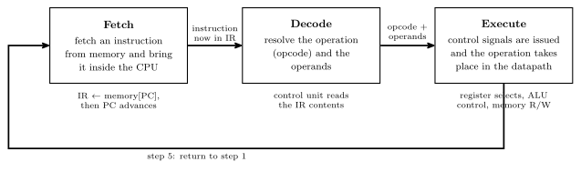
Figure 54: The cycle as a loop: a three-stage pipeline. Each box holds a one-line description of its stage, each arrow carries what the stage leaves behind for the next one, and the notes under the boxes summarise steps 1–4 above.
Step 2 advances the PC before the instruction executes, which is why a jump instruction works by overwriting the PC rather than by suppressing the increment.
The datapath
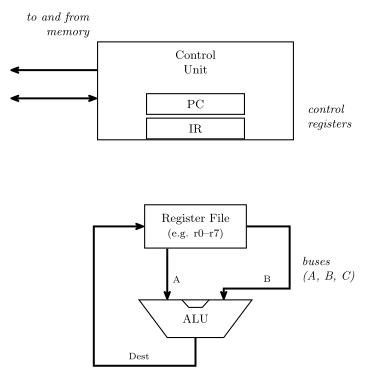
Figure 55: The datapath the cycle runs on. The control unit holds PC and IR and talks to memory; below it, the register file puts two values onto the A and B buses, the ALU combines them, and the result returns on the destination bus to be written back into a register.
The question this raises — and the one the control unit exists to answer — is how do we control this? Specifically:
- How do we tell the ALU what to do?
- How do we choose what register values are placed on the A and B buses?
- How do we choose which register receives the result from the destination bus?
- How do we know when to read or write memory?
Control signals
Each of those questions is answered by a bundle of wires out of the control unit. For a machine with 8 registers and the ALU of arithmetic-logic-unit:
| Signal | Width | Answers |
|---|---|---|
| A register select | 3 | which register drives the A bus (\(2^3 = 8\) registers) |
| B register select | 3 | which register drives the B bus |
| Destination select | 3 | which register the result is written back into |
| ALU control | 6 | what the ALU does — \(F_1\), \(F_0\), ENA, INVA, ENB, INC |
| Memory read/write | 1 | whether this is a read or a write |
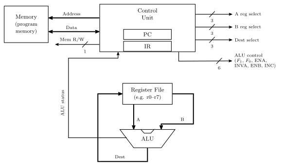
Figure 56: The same datapath with every control signal named. Added to the previous figure: the memory block, the Address, Data and Mem R/W labels, the five bundles with their widths, and the ALU status path back into the control unit. The bundles are drawn as labelled stubs: A/B/Dest select drive the register file, ALU control drives the ALU. Widths are marked with a slash and a number; the course also letters the width beside a plain arrow, and neither is fixed as the standard. Everything except the memory block sits inside the CPU.
Plus the address and data connections to memory itself. The widths are not arbitrary: three bits because there are eight registers, and six bits because the ALU has exactly six control inputs.
Control signals come from the control unit, which must generate them in the right order for a given instruction — and which instruction that is, is determined by the contents of the Instruction Register.
So a line of high-level code like r5 = r0 + r2 becomes: A select = 0, B select = 2, destination select = 5, ALU control = the \(A + B\) row of the combinations table, memory read/write idle.
Data influencing control
The IR is not enough. The control unit can’t operate without knowing something about the data — for example, if a for-loop variable is supposed to count from 10 down to 0, how does the control unit know when it gets there?
The answer is the status register: determined by ALU operations, it stores the status of the last ALU operation and is available to the control unit. This closes the loop — the ALU’s results feed back into the control unit and change what it does next, which is what makes conditional branching possible at all. It is the return path drawn in Figure 56, and it is what a source-level if (x < 0) compiles down to.
ALU status flags
The ALU emits, alongside its result, a summary of what happened during the last operation. Typically stored in a special purpose register called the STATUS register:
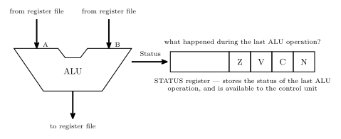
Figure 57: The ALU’s second output. The result goes back to the register file; alongside it the ALU reports what happened, and those flags land in the STATUS register where the control unit can read them. The ALU is drawn as a notched trapezoid here; the block diagram in the ALU note draws the same block as a plain rectangle, and the course uses both shapes. The register is drawn as four named cells at the right-hand end of a wider register. That is shorthand, not a bit-position claim — the AVR’s own SREG orders and numbers its bits differently, see the AVR architecture note.
| Flag | Name | Asks |
|---|---|---|
| Z | zero | was the last result 0? |
| V | overflow | did the last addition/subtraction overflow, assuming it was a two’s complement operation? |
| C | carry | was a carry out generated? |
| N | negative | was the result negative if considered as two’s complement — i.e. what is the sign bit? |
V and N both presuppose a two’s complement interpretation while C does not — the hardware computes all four regardless, and it is the program’s business to read the ones that mean something for the operation it just did. See binary-number-representations, and 2026-08-04-binary-arithmetic for the overflow rules V implements.
Worked example
What values are in the status register flags after the operation \(8_{10} - 9_{10}\) on a 5-bit ALU?
First, \(-9\) in 5-bit two’s complement: \(9 = 01001\), invert to \(10110\), add one to get \(10111\). Then add, tracking the carry into and out of the sign column:
\[\begin{array}{crl} \text{carry into MSB} \rightarrow & 0\phantom{0000} & \\ & 01000 & \\ + & 10111 & \\ \hline \text{carry out} = 0 \rightarrow & 11111 & \end{array}\]
The result is \(11111\), with no carry out of the top bit. So:
| Flag | Value | Why |
|---|---|---|
| Z | 0 | the result \(11111\) is not zero |
| C | 0 | no carry out of the most significant bit |
| V | 0 | the carry into the sign column and the carry out of it agree, both 0 — and indeed \(8 + (-9) = -1\) is comfortably in range for 5-bit two’s complement |
| N | 1 | the sign bit is 1 — the result is negative |
And indeed \(11111\) read as two’s complement is \(-1\), which is \(8 - 9\).
See also
- cpu-organisation · arithmetic-logic-unit
- binary-number-representations — two’s complement, overflow and the sign bit
- 2026-08-04-binary-arithmetic — the \(C_{in} \oplus C_{out}\) overflow test the V flag implements
- avr-architecture — the AVR’s own status register, bit by bit
- state-machines — the control unit is itself a state machine, sequencing signals for each instruction
- 2026-08-24-alu-and-control-unit — Lecture 9
The I/O Board
The I/O board in the lab kit carries the input and output devices you wire your breadboard circuits to, for experimenting with simple digital circuits. It plugs directly onto the breadboard, and adds a logic probe for debugging and a UART serial interface for talking to other devices.
It is powered from a single USB connection and has current-sense circuitry that detects short circuits and protects your designs.
Pin numbers for every device are in device-pinouts; the kit itself is loaned out in week3-lab-logisim-and-flip-flops. Two more parts of the kit that are used alongside the board, the joystick and the LED matrix, are described at the end.
What’s on it
| 1. USB connector | 2. Power LED | 3. Power switch | 4. 7-segment display |
| 5. Switches | 6. LEDs | 7. Buttons | 8. UART transmit/receive LEDs |
| 9. Logic probe indicator LEDs | 10. Fault LED | 11. VCC / GND headers | 12. I/O device headers |
| 13. Auxiliary power connector | 14. High current mode jumper |
Items 13 and 14 are the auxiliary power connector and the high-current-mode jumper. The one extra power connection the labs use is connector J1, which powers the LED matrix in Lab 16 (below).
The board at a glance
The board is a C shape: a left-hand spine carrying the USB connector, the power switch, the two status LEDs and the seven-segment display, plus a top arm and a bottom arm that straddle the breadboard’s central channel. All the I/O devices come out on the two 16-pin headers on the inner edges of those arms, and every device is reached through the column of breadboard holes directly above or below its printed label.
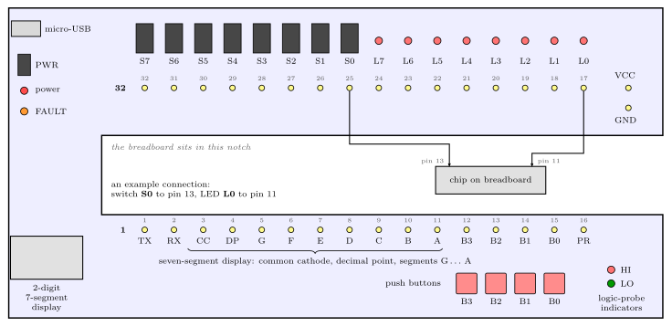
Figure 58: A plan view of the board, not to scale, with the parts on the left spine placed roughly. Each I/O device sits on one pin of one of the two 16-pin headers, and the column of breadboard holes at that pin is how you reach it. The board itself prints only the two end markers, a bold 32 at the left of the top header and a bold 1 at the left of the bottom one. The small numbers at the other pins are their pin numbers, the ones a schematic uses. The connection drawn in the notch is an example: switch S0 to pin 13 of a chip, LED L0 to pin 11.
Two things about the numbering are worth fixing in your head before you wire anything:
- The top header counts down, left to right. Its leftmost pin is 32 and its rightmost is 17, so the switches run
S7…S0and then the LEDsL7…L0as you read left to right. That is the opposite of the reading order you would guess from the pin numbers alone. - The bottom header counts up, left to right, pin 1 to pin 16:
TX RX CC DP G F E D C B A B3 B2 B1 B0 PR. The middle nine of those are the seven-segment display —CCits common cathode,DPits decimal point, andGdown toAits seven segments — which is why nine consecutive pins carry single-letter names.
VCC and GND pads sit at the far right of both arms, which is where the breadboard’s power rails get fed from.
Setup
Insert the board into the breadboard, aligning the downward-facing headers with the right holes.
If aligned correctly, the I/O board should not require excessive force to insert.
Connect a micro-USB cable to the connector at the top-left corner.
DO NOT STORE THE BOARD WITH THE USB CABLE ATTACHED — THIS MAY CAUSE THE USB CONNECTOR TO BREAK OFF!!
The USB connector is the part people break.
Turn the board on by sliding the PWR switch up to ON; the red power LED should light. Then check the orange FAULT LED does not light. If it does, power off immediately.
The fault LED
The board uses a current-limited power switch to protect itself and anything it powers from short circuits. A short lights the orange FAULT LED.
If it’s on: push PWR down to OFF immediately, and check your design for shorts before restoring power.
WARNING! In the case of a short circuit, the current-limiting switch may become extremely hot.
The logic probe
Attach a wire to the column of terminals above the PR label — pin 16, the rightmost pin of the bottom header. Touch the free end to any point in the circuit and the HI / LO LEDs show the logic state there.
As circuits increase in complexity, so does the necessity of having a clear strategy — probing random points in a large circuit rarely reveals the location of errors.
Suggested troubleshooting strategy
- Check the FAULT light is not on, which would indicate a short circuit.
- Probe VCC and GND at every device in your circuit, to confirm each one is actually powered.
- Start at the inputs and move logically through to the outputs. Pen and paper helps: write down the expected state at each point first, then verify it with the probe. A schematic and a truth table are great for this.
The key to any successful debugging strategy is to assume nothing, know what to expect before you begin testing, and have a plan.
Step 2 is the one worth internalising — an unpowered chip looks exactly like a wrong-logic chip until you probe its power pins, and grouped VCC/GND entries on a schematic (see circuit-schematics) make it easy to forget one.
Electrical characteristics
| VCC | 5 V |
| GND | 0 V |
| Logic high | > 3.5 V |
| Logic low | < 1.5 V |
The gap between 1.5 V and 3.5 V is undefined, which is why a floating pin can read as either (week3-lab-logisim-and-flip-flops). What the logic probe shows for a voltage inside that band is not documented.
The joystick
The kit’s two-axis joystick is a small board of its own, made to sit in the breadboard next to the I/O board. Each axis is a potentiometer between its own supply pin and ground, and the stick moves the wiper. So each axis gives a voltage that follows the stick across its travel, from 0 V at one side to 5 V at the other, for the A/D converter to read (analog-to-digital-conversion).
| Pin | What it is | Connect to |
|---|---|---|
| L/R+ | top of the left-right potentiometer | VCC |
| U/D+ | top of the up-down potentiometer | VCC |
| GND ×2 | bottom of both | GND, either one |
| L/R ×2 | x: 0 V with the stick to the left, 5 V to the right | an analog input, either one |
| U/D ×2 | y: 0 V at the bottom, 5 V at the top | an analog input, either one |
- The doubled pins are joined on the board. One wire to each of L/R, U/D and GND is enough.
- The two
+pins are separate. Both have to go to VCC, or one axis has nothing to divide. - Left, right, up and down are the joystick’s own, marked by the X and Y arrows printed on it. Placed at the right-hand end of the breadboard, with room for the microcontroller board and programmer to its left, the X arrow points to the top of the breadboard and the Y arrow to the left.
- A potentiometer’s wiper is a weak source. Anything that draws current from it, an LED for instance, pulls its voltage away from the stick’s position. LEDs make a quick wiring test, but they must come off before the converter is used.
- Keep the black foam that protects the pins when the joystick is put away.
Figure 59: The joystick’s eight pins, seen from above with the board placed as it sits in the breadboard, its X arrow pointing to the top. The pins near each corner come in twos. The dashed lines join the pins that are connected on the board itself: the two L/R pins, the two U/D pins and the two GND pins, so one wire to each pair is enough. The two supply pins, U/D+ at the top left and L/R+ at the bottom left, are not joined, and both go to VCC. L/R carries x and U/D carries y to the analog inputs.
The LED matrix
The LED matrix is a display of 16 columns by 8 rows, each pixel a red LED and a green LED together. It is driven over SPI: the AVR is the master and the matrix a slave that takes commands one byte at a time (avr-spi).
Connecting it
It has two headers:
- K1, two pins, is its power. A two-wire lead joins it to the I/O board’s connector J1, VCC on J1’s left pin and GND on its right.
- K2, four pins, is the SPI connection, to the AVR’s SPI port on PB7 to PB4: SCK on PB7, MISO on PB6, MOSI on PB5 and \(\overline{\text{SS}}\) on PB4. Match the order of the pins on K2 against the datasheet before plugging the lead in.
The Err state. PB7 to PB5 are also the pins the programmer uses to load the AVR, so programming sends the matrix a stream of what look to it like garbage commands, and it can show Err. Holding the AVR’s reset button down for at least half a second after programming clears it before the program starts.
What to send it
Every message starts with a command byte. Two commands are enough to draw anything:
| Command | Bytes | Does |
|---|---|---|
| clear | 0x0F |
every pixel off |
| set one pixel | 0x01, position, colour |
sets one pixel to a colour |
- Position byte:
(y << 4) | x. The row y, from 0 at the bottom to 7 at the top, is the high nibble. The column x, from 0 at the left to 15 at the right, is the low nibble. - Colour byte:
(green << 4) | red. Each nibble is a brightness from 0 to 15. Red alone is0x0F, green alone0xF0, both full is yellow,0xFF, and full red with half green is orange,0x7F.
The matrix’s reference manual is the full description of the commands it accepts.
Figure 60: How a pixel is addressed and coloured. The matrix is 16 columns, x from 0 to 15 left to right, by 8 rows, y from 0 to 7 bottom to top. A position byte puts y in its high nibble and x in its low one, so the pixel at x = 4, y = 2 is 0x24. A colour byte puts the green brightness in its high nibble and the red in its low one, each 0 to 15. The swatches show what some colour bytes look like: the colours here are the light from the red and green LEDs mixed.
Lab 16 works through the commands and uses them for a demo, a scrolling marquee across two matrices and an Etch-A-Sketch (week10-lab-adc-and-spi).
See also
- device-pinouts — the pin table behind Figure 58, and the board’s schematic symbols
- circuit-schematics — how the board is drawn on a schematic (
IO1/IOBOARD, input and output pentagons) - avr-io-ports — the same switches and LEDs driven from an AVR rather than from gates
- week3-lab-logisim-and-flip-flops — where the kit is loaned out
- week10-lab-adc-and-spi — Lab 16: the joystick read by the A/D converter, and the LED matrix driven over SPI
- analog-to-digital-conversion · avr-spi — the two AVR peripherals the joystick and the matrix are used with
Memory Models
The first of the four things that make up an ISA (instruction-set-architecture): how memory looks to the CPU. Four issues decide that — addressable cell size, alignment, address spaces and endianness — and every one of them is a decision the specification has to make, not something the hardware settles on its own.
Memory as addressable cells
Computer memory is conceptually a set of addressable cells:
- Each cell has a unique address (or cell number).
- Cells are usually 8 bits wide (i.e. hold one byte).
- Various cell widths have been used in the past — 8 bits is a convention, not a law.
Drawn as a table, the address indexes the rows and the cell width is how wide each row is:
| Address | ← cell width → |
|---|---|
| 0 | |
| 1 | |
| 2 | |
| 3 | |
| … |
A “4 × 3 memory” in that notation means 4 addresses of 3-bit cells — and \(4 = 2^2\), so two address bits. Built at gate level, it shows that “memory” at this level is nothing more exotic than flip-flops-and-latches and combinational-logic-blocks arranged into storage.
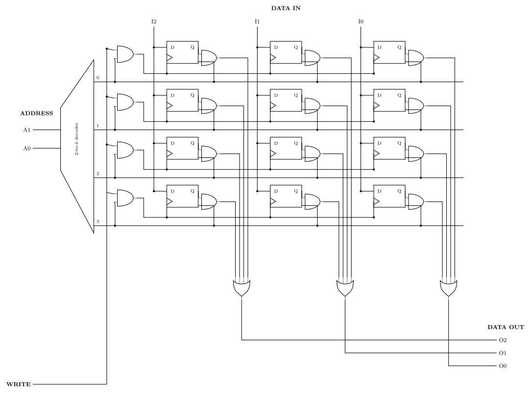
Figure 61: A 4 × 3 memory at gate level — four addresses of three-bit cells. Twelve D flip-flops in four rows of three: one row is one addressable cell. The decoder turns A1 A0 into exactly one row-select (word) line. Writing: the word line ANDed with WRITE clocks that row’s three flip-flops, so DATA IN (I2 I1 I0) — which is wired to every row’s D inputs all the time — is captured only by the selected row. Reading: each flip-flop’s Q is ANDed with its own word line and the three cells of a column are OR’d together, so the unselected rows contribute 0 and DATA OUT (O2 O1 O0) carries the selected row alone. The decoder is drawn as a trapezoid with the wide edge on the right, and the flip-flops as plain rectangles with a clock wedge on the lower-left edge, per this course’s conventions (csse2010-diagram-notation). The most significant bit, I2/O2, is the leftmost column.
A. Addressable cell size
Most common cell size is 8 bits (1 byte) — but not always.
The AVR is the counterexample sitting on the bench:
| AVR memory | Cell width |
|---|---|
| Data memory | 8 bits |
| Instruction (program) memory | 16 bits |
Which is why an AVR instruction is “one word” rather than “two bytes” — a program-memory address counts 16-bit cells.
The bus transports the content of a cell, but the data bus may be wider than one cell: it can retrieve several cells (addresses) at once. When it does, the address bus does not need to be as wide.
Bus sizes
For every doubling of the data bus width, remove the least significant bit of the address bus.
For a memory of \(2^n\) cells at 8 bits per cell — so an address size of \(n\) bits:
| Data bus | Address bus | Cells per transfer |
|---|---|---|
| 8 bits | \(n\) bits | one cell at a time |
| 16 bits | \(n-1\) bits | two cells at a time |
| 32 bits | \(n-2\) bits | four cells at a time |
The reason is that a wide transfer always moves an aligned group of cells. With a 16-bit data bus the memory only ever hands over cell pairs \((0,1), (2,3), (4,5), \dots\) — so the bottom address bit never selects anything, and naming the pair takes one bit fewer than naming the cell.
Worked example. A memory of 64 cells, 8 bits each, addressed 000000 … 111111:
\[64 = 2^6 \text{ cells} \implies 6\text{-bit addresses}\]
| Data bus | Address bus |
|---|---|
| 8 | 6 |
| 16 | 5 |
| 32 | 4 |
Read the two buses as a pair, not separately: widening one narrows the other by exactly as much.
Word addresses and byte addresses
The AVR’s 16-bit program-memory cells have one practical consequence. The program counter, jmp, call and every code label count words. But a table of constant bytes kept in flash is read a byte at a time by lpm, load program memory, and lpm takes a byte address in the Z register. Word \(w\) holds bytes \(2w\) and \(2w + 1\), with the low byte at the even address, which is the AVR being little endian (section D).
So turning a code label into a byte address means doubling it. Take the string Hello stored at word 2 by mesg: .db 72,101,108,108,111 (assembly-process):
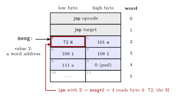
Figure 62: One region of program memory addressed two ways. Each row is a 16-bit word, numbered on the right, and each half is a byte, numbered inside its cell. The label mesg has the value 2 because labels in the code segment count words. Byte addressing counts the halves, low byte first, so word 2 starts at byte 4. That is why lpm is pointed at mesg*2: with Z = 4 it loads 72, the H. The five bytes of the string take two and a half words, and the last half word is a zero pad. Grey marks the jmp, blue the string and red the byte that lpm reads.
        ldi  ZH, high(mesg*2)   ; Z = 4: byte address of word 2
        ldi  ZL, low(mesg*2)
        lpm                     ; r0 <- 72, the H
Leaving out the *2 points Z at byte 2, the low byte of word 1, which is half of the jmp.
B. Alignment
Many architectures require natural alignment, e.g.
- 4-byte words starting at addresses 0, 4, 8, …
- 8-byte words starting at addresses 0, 8, 16, …
i.e. an \(n\)-byte value must start at an address that is a multiple of \(n\).
Taking an 8-byte word on a machine that fetches 8 bytes at a time:
| Where it sits | Reads needed | |
|---|---|---|
| Aligned | bytes 8–15, i.e. an 8-byte word at address 8 | 1 — it is exactly one fetched block |
| Non-aligned | bytes 12–19, i.e. an 8-byte word at address 12 | 2 — the top half of block 8–15, plus the bottom half of block 16–23 |
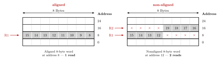
Figure 63: An aligned and a non-aligned 8-byte word. Four blocks of eight bytes; grey marks the bytes of the 8-byte word. On the left the word starts at address 8, so it is one block — one read. On the right it starts at address 12, so it takes the top half of the block at 8 and the bottom half of the block at 16 — two reads, marked R1 and R2. Two things about the drawing: addresses increase upward (unlike every other memory figure in the course, where they increase downward — see csse2010-diagram-notation on that inconsistency), and byte numbers within a row run high-to-low left to right. The × marks a byte in the fetched block that is not part of the word.
Alignment is often required because it is more efficient — the aligned case is always one read, the non-aligned case sometimes two, and the hardware that stitches two blocks together and extracts the middle is hardware that a machine demanding alignment simply does not need.
When alignment is not required — the Pentium IV
- Fetches 8 bytes at a time from memory (64-bit wide data bus).
- Alignment is NOT required, so the processor stays backwards compatible with earlier processors.
- A 4-byte word stored at address 4 takes 1 read (bytes 0 to 7).
- A 4-byte word stored at address 6 must read bytes 0 to 7 (one read) and bytes 8 to 15 (second read), then extract the 4 required bytes from the 16 bytes read.
Counting reads in general
A data bus \(w\) bytes wide delivers one aligned \(w\)-byte block per read. An \(n\)-byte value starting at address \(a\) therefore costs
\[\left\lceil \frac{(a \bmod w) + n}{w} \right\rceil \text{ reads}\]
The best case is \(n/w\) (rounded up), when the value starts on a block boundary; every other starting offset can push it one block further. So a value read from an arbitrary address costs either \(\lceil n/w \rceil\) or one more than that — which is why questions of this shape almost always answer “\(k\) or \(k+1\)” rather than a single number.
Worked example: an 8-byte value on a 16-bit data bus, no natural alignment required. Here \(w = 2\) and \(n = 8\):
| Starting address | Spans | Reads |
|---|---|---|
| Even | 4 aligned 2-byte blocks | 4 |
| Odd | 9 byte-positions, so 5 aligned blocks | 5 |
so the answer is 4 or 5. The odd case is the one to picture: one byte of the value sits alone at the top of the first block and one byte alone at the bottom of the last, and each of those still costs a whole read.
C. Address spaces
Many microprocessors have a single linear memory address space — the von Neumann architecture:
- e.g. \(2^{32}\) bytes numbered from 0 to \(2^{32} - 1\).
- (These may not be bytes — it depends on the addressable cell size.)
- Program and data share the one space.
However, the Harvard architecture has separate address spaces for instructions and data. The same numeric address means a different location depending on which space you are in, and an instruction says which one it means by what instruction it is.
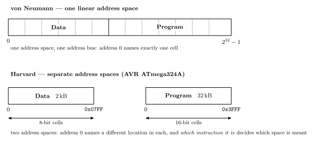
Figure 64: The two address-space models. Above: von Neumann — one linear space, so program and data are separated only by convention and address 0 names exactly one cell. Below: Harvard, in the AVR ATmega324A’s shape — two spaces, each starting at its own 0, with different sizes and different cell widths — and the cell width under each box is the whole reason the arithmetic below works out the way it does: 32 kB of program memory is \(2^{15}\) bytes but only \(2^{14}\) addresses, because each address there names a 16-bit cell. The end addresses follow from the sizes, so the data box ends at 0x07FF (\(2^{11}-1\), for 2048 bytes) rather than the 0x08FF of Figure 65, which is that 2 kB plus the 256 locations in front of it.
AVR ATmega324A is Harvard:
| Space | Size | Address width |
|---|---|---|
| Data | \(2^{11}\) (2048) bytes | 11 bits |
| Instruction | \(2^{14}\) 16-bit words — 16,384 instruction words = 32,768 bytes | 14 bits |
The arithmetic — convert to cells first, then take the logarithm:
\[\text{data: } 2\,\text{kB} = 2 \cdot 2^{10}\,\text{B} = 2^{11} \text{ cells (8-bit)} \implies 11 \text{ bits}\] \[\text{program: } 32\,\text{kB} = 2^{5} \cdot 2^{10}\,\text{B} = 2^{15}\,\text{B} = 2^{14} \text{ cells (16-bit)} \implies 14 \text{ bits}\]
The program-memory step is the one that catches people: 32 kB of flash is only \(2^{14}\) addresses, not \(2^{15}\), because each address names a 16-bit cell. Halve the byte count before taking the log whenever the cells are not bytes.
Laid out as a memory map (see avr-architecture for the rest of the chip):
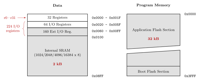
Figure 65: The ATmega324A’s two address spaces. Lowest address at the top, hex addresses outside on the right, grey fill on the coarsely-described regions, and the diagonal break across the flash meaning not to scale: that is this course’s memory-map convention (csse2010-diagram-notation). Marked in red: the register file is r0–r31, the 64 I/O plus 160 extended I/O registers are the 224 of avr-io-ports, the SRAM is 2 kB and the flash 32 kB.
Two details worth pinning down. 0x3FFF \(= 2^{14} - 1\), which is the 14 bits above. And the data space runs to 0x08FF — that is the 2 kB of SRAM plus the 256 locations (0x0000–0x00FF) that the register file and I/O registers occupy in front of it; the “\(2^{11}\) bytes” above is the SRAM itself, which is what the 11 bits size.
The assembler’s view: segments
An assembler treats each address space as a segment with its own location counter (assembly-process). On the ATmega324A there are three, because the EEPROM is a third address space alongside the two above:
| Segment | Directive | Address space | Cell | Counter starts at | The assembler can |
|---|---|---|---|---|---|
| code | .cseg |
program memory, flash, 32 kB | 16-bit word | 0x0000 |
place instructions and constants |
| data | .dseg |
data memory, SRAM | byte | 0x0100 |
only reserve space |
| EEPROM | .eseg |
EEPROM, 1 kB | byte | 0x0000 |
place constants |
Three consequences of separate spaces:
- The same number means different places. Address 0 is the reset
jmpin the code segment, registerr0in data memory and the first EEPROM byte in the EEPROM segment. - The units differ.
.org 0x0100in the code segment is word 256, which is bytes 512 and 513 of flash. In the data segment it is byte0x0100. - The data counter does not start at 0. The first 256 data addresses are the registers and I/O registers of Figure 65, so the first variable lands at
0x0100.
The data segment can only be reserved, not filled, because the assembler’s output is programmed into flash and EEPROM, which keep their contents, while SRAM starts empty at every power-up.
The memory behind each space
The three spaces are three different kinds of memory, and the kind explains how each is used (memory-technologies):
| Space | Technology | Volatile? | Erased and rewritten |
|---|---|---|---|
| Program memory | flash | no | electrically, a block at a time |
| Data memory | SRAM, flip-flops | yes | written a byte at a time, freely |
| EEPROM | EEPROM | no | electrically, one cell (byte) at a time |
The flash is divided into two blocks, the Application Flash Section and the Boot Flash Section of Figure 65. Because flash is erased a block at a time, a boot loader in the boot section can erase and rewrite the application section without erasing itself. Other AVR devices have one flash block, and some have more.
The register file and the SRAM sit at the top of the memory hierarchy. Unlike a desktop processor, the AVR has no cache: its SRAM is small enough and fast enough to keep up with the CPU directly.
D. Endianness
Different machines may support different byte orderings for a multi-byte value.
| Which end goes first (at the lowest address) | Used by | |
|---|---|---|
| Little endian | the little end — least significant byte | Intel microprocessors (Pentium etc.), and AVR |
| Big endian | the big end — most significant byte | SPARC, Freescale (formerly Motorola) microprocessors |
Most desktop/workstation/server CPUs produced since ~1992 are “bi-endian” (support both) — some switchable at boot time, others at run time, i.e. they can change dynamically.
Endianness only ever matters when a value spans more than one cell: reassembling it means knowing which cell was the low-order one.
Worked example
Given this memory:
| Address | Contents |
|---|---|
| 0 | 00001111 |
| 1 | 00110011 |
| 2 | 11011101 |
| 3 | 00101100 |
| Read | Value | Why |
|---|---|---|
| the 1-byte word at address 1 | 00110011 |
one cell — endianness does not apply |
| the 2-byte word at address 0, big endian | 00001111 00110011 |
big end first, so address 0 holds the most significant byte |
| the 2-byte word at address 2, little endian | 00101100 11011101 |
little end first, so address 2 holds the least significant byte and address 3 the most |
The mechanical way to do these without getting turned around: write the addresses the value occupies in increasing order, then assemble the answer most-significant-byte first. Big endian reads the addresses forwards; little endian reads them backwards.
See also
- instruction-set-architecture — the four pillars this is the first of
- avr-architecture — the ATmega324A’s two address spaces in full
- addressing-modes — how an instruction names a memory location
- binary-number-representations · flip-flops-and-latches · combinational-logic-blocks
- assembly-process — segments, location counters, and
.dbpacking two bytes to a word - compilation-and-linking — where a C compiler puts globals, locals and the heap in data memory
- memory-technologies — flash, SRAM and EEPROM as technologies, and why sizes are powers of 2
- memory-hierarchy-and-cache — registers, cache, main memory and disk, by speed and cost
- 2026-08-31-instruction-set-architecture-part-1 — Lecture 11 · 2026-10-08-assembly-process — Lecture 20 · 2026-10-22-memory-disks-and-files — Lecture 24
Polling and Interrupts
How a CPU finds out that an I/O device needs attention: by asking (polling) or by being told (interrupts). This note covers what an interrupt does to the flow of control, the three problems any interrupt mechanism has to solve, the fourteen steps from a device’s request to the resumed program, transparency, what to do about a second interrupt, and traps, the software counterpart. First met in 2026-09-21-interrupts. How the AVR implements it (its vector table, the ISR in assembly and in C, and the registers that switch an interrupt on) is avr-interrupts.
The problem
The CPU is fast, and I/O is slow and asynchronous. At 8 MHz the AVR completes an instruction every one or two clock cycles, while a key is pressed, a character arrives or a timer matches on its own schedule. That schedule has no relation to the clock or to which instruction the program is on. The CPU needs to know two things:
- when data is available from an input device, and
- when an output device is ready to accept data.
There are two ways to find out: polling-driven I/O and interrupt-driven I/O.
Polling
The processor periodically asks each device whether it is ready, and waits for the answer. On the AVR, asking is reading a register: a pin in PINx (avr-io-ports), or a flag in a timer’s TIFRn (avr-timers-and-counters). A polling program is a main loop that asks each device in turn:
while (1) {
    if (PINC & (1<<0)) {            /* is the button pressed?  */
        /* ... handle the button ... */
    }
    if (TIFR1 & (1<<OCF1A)) {       /* has the timer matched?  */
        TIFR1 = (1<<OCF1A);         /* clear the flag          */
        /* ... handle the tick ... */
    }
    /* ... everything else the program does ... */
}
It is inefficient, in two ways:
- Time spent asking. Most asks find nothing, and every one of them costs instructions.
- Time spent waiting. An event is noticed only at the next ask, so the delay before it is handled can be as long as one pass of the loop. Every piece of work added to the loop lengthens that pass, and so slows the response to every device.
But it may be fine if the processor has nothing else to do. A program whose only job is to wait for a button and then act gains nothing from anything cleverer. Polling is also simple: the program always knows exactly where it is, and nothing happens behind its back.
Interrupts
The device tells the CPU when it is ready. The three kinds of ready:
| Kind | Example |
|---|---|
| Device ready to accept more output | the serial transmit buffer is empty |
| Device has input ready | a key pressed on a keyboard |
| A regular interrupt | a timer generating an interrupt every, say, 20 ms |
When the request arrives, the CPU finishes its current instruction, sets the running program aside, and runs a routine for that device, the interrupt handler or interrupt service routine (ISR). When the handler completes, control returns to where the program left off. The interrupted program does not ask, wait, or even know.
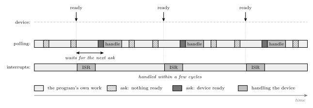
Figure 66: The same three device events handled both ways. Polling: the CPU breaks off its own work at fixed intervals to ask whether the device is ready. Most asks find nothing (hatched), and an event waits for the next ask before it is noticed, so how quickly it is handled depends on how often the program asks. Interrupts: the CPU does its work without asking, and each event diverts it into the handler within a few cycles. No time is spent asking, and the response does not depend on how long the main loop is. The work done is the same in both rows; what differs is the time wasted asking and the delay before each event is handled.
Interrupts are more efficient for the CPU, and they change the flow of control, which is where their cost lies.
A fourth way to leave the sequence
Normally the PC just increments. avr-branches-and-jumps and procedures-and-the-stack cover the instructions that change it. An interrupt changes it too, but without any instruction asking:
| Triggered by | Where the new PC comes from | Comes back? | |
|---|---|---|---|
| Branch | an instruction, if a flag says so | an offset in the instruction | no |
| Jump | an instruction | the instruction | no |
| Procedure call | an instruction (call) |
the instruction | yes: ret pops the return address call pushed |
| Interrupt | a device, between any two instructions | a table, indexed by which device | yes: the return-from-interrupt instruction pops the address the hardware pushed |
| Trap | an instruction that produces an exceptional result | a table, indexed by which error | not always |
The useful way to see an interrupt is as a procedure call that the hardware makes. The mechanism is the same: push the return address, load the PC, and pop it back at the end. The difference is that the program never asked for it, and that one difference produces all three of the issues below.
The three issues
Any interrupt mechanism has to answer three questions.
- How does the CPU know where the ISR is? A call names its target, but an interrupt does not, so the address must be found from the source. The CPU looks in an interrupt vector table, often at the beginning of memory. The table holds either the address of each handler, which the CPU loads into the PC, or a jump instruction to each handler, in which case the CPU loads the PC with the entry’s own address and executes the jump. The AVR does the second. Vector is used both for the interrupt’s number (its index in the table) and for the address of its handler, and it is worth checking which is meant.
- How are the registers preserved? All of them, including the status register. The handler must save copies of any register it uses before using it, and restore them before it returns. Many CPUs save the status register automatically; the AVR does not, so the handler must save it itself if it would change it. The result is transparency, below.
- What happens if another interrupt arrives while one is being serviced? Either it waits, or it interrupts the handler. See Nesting and priority, below.
The sequence of actions
From the device’s request to the resumed program there are fourteen steps, shared between the hardware and the ISR:
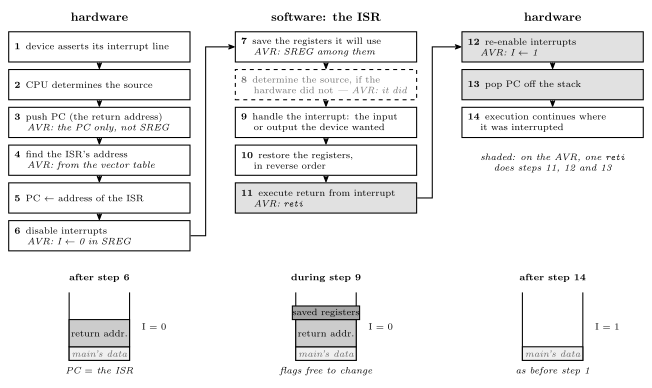
Figure 67: The fourteen steps of an interrupt, in the three phases the hardware and the ISR take turns at, with the state of the machine after each phase underneath. The hardware does the first six: it saves only the return address, finds and enters the handler, and turns interrupts off. The ISR saves what it will use, does the I/O and restores what it saved. The return-from-interrupt instruction then hands back to the hardware, which turns interrupts on and pops the return address. The notes in italics are the AVR’s version of each step. The shaded steps 11 to 13 are a single AVR instruction, reti, and step 8 rarely arises on the AVR (dashed), because every source has its own vector and so the ISR knows which one fired; only a pin-change handler, whose vector covers a whole port, still has to find which pin changed. The stack after step 14 is exactly as it was before step 1, and that is what transparency requires.
Three things in the sequence are worth holding on to:
- The hardware saves as little as it can. It pushes only the return address, and everything else is the ISR’s job. That keeps the entry fast, and it means an ISR that uses nothing need save nothing.
- Interrupts are off from step 6 to step 12. That is the default answer to issue 3: a second request simply waits until the handler has returned. On the AVR, off is the I bit of the status register being 0 (avr-architecture).
- Return from interrupt is not the same as return from procedure. It has to undo step 6 as well as step 3. A handler that ends with a plain
retgoes back to the right place but leaves interrupts disabled for good.
Transparency
When the ISR finishes, the computer is in the same state as it was before the interrupt. That is transparency, and it is the answer to issue 2. It matters more for an ISR than for a procedure because the interrupted code has no chance to prepare. A caller knows where its calls are and can agree with the procedure which registers it may use. An interrupt can land between any two instructions, including these two:
    cp   r16, r17        ; sets Z if r16 == r17
                         ; <- an interrupt here
    breq equal           ; reads Z
If the ISR does anything that sets flags — a dec, an andi, a cp of its own — and does not restore the status register, breq reads the ISR’s Z instead of the one cp produced. The program then takes the wrong branch, but only on the rare occasions the interrupt lands in that one gap. A bug like that can survive a great deal of testing. So the status register is the one register a handler must always consider, even if it touches nothing else. Whether an instruction changes it is listed per instruction in the instruction set reference (avr-instructions).
Nesting and priority
For an interrupt that arrives while an ISR is running, there are three policies:
- Disable interrupts during an ISR. The simplest: the second request waits (its flag stays set) and is serviced after the first handler returns. On CPUs that save the status register automatically, the global interrupt enable flag is among the bits the return-from-interrupt instruction restores, so it comes back on by itself. This is the AVR’s default.
- Prioritise. Higher-priority interrupts may interrupt lower-priority handlers, but not the other way round and not at the same level. Urgent devices are never kept waiting behind unimportant ones, and an unimportant device can never delay an urgent one. Many CPUs support this; the AVR does not.
- Re-enable interrupts inside the ISR. Any interrupt may then interrupt the handler, regardless of priority. The AVR allows this if the handler executes
sei.
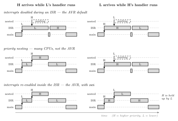
Figure 68: The three policies for an interrupt that arrives while another is being handled, in the two cases that tell them apart. In each panel, code on a higher lane has interrupted the code below it, and a dashed box is a request that is waiting. With interrupts disabled during an ISR, whichever handler started first finishes first, and the other waits for it in both cases. With priority nesting, the urgent request (H) cuts into the less urgent handler (L) but never the reverse, which is the behaviour one would want and the one the AVR does not provide. With interrupts re-enabled inside the handler, any request cuts in immediately, so in the right-hand case the urgent handler is itself held up by the less urgent one.
On the AVR, then, priority only decides the order in which waiting interrupts are serviced. It matters only when two or more are waiting at once, for instance because they arrived during another handler. The highest-priority one, the one with the lowest vector, goes first. It never lets an urgent interrupt cut into a running handler. The one way to get nesting is to re-enable interrupts inside the handler, and then priority plays no part at all. Both cases are traced, with the I bit, in 2026-09-21-interrupts.
The practical consequence is a rule: keep ISRs short. While any handler runs, every other interrupt waits. A handler that busy-waits for 10 ms delays every other device by 10 ms, and a timer tick that arrives twice during that time is serviced only once, because a flag can record that an event happened but not how many times.
Traps
Traps are software interrupts: interrupts caused by events in the software rather than in the hardware, and specifically by exceptional events, such as
- overflow,
- divide by zero, and
- an undefined opcode.
They relate to error checking the way interrupts relate to polling. Without traps, a program that must not overflow has to test after every arithmetic instruction, which is polling for errors. With them, the hardware watches, and the program is diverted only when the error actually happens. Traps save continually checking for errors.
Trap handlers don’t always return to the original program. After a division by zero or an undefined opcode, there is often no sensible instruction to continue with. Under an operating system the usual outcome is that the program is ended.
| Interrupt | Trap | |
|---|---|---|
| Caused by | a device, outside the program | the instruction being executed |
| When | at an unpredictable point in the program, asynchronously | at the same instruction every time, given the same data |
| Returns? | always, to the interrupted instruction’s successor | not always |
The AVR does not provide traps. Overflow sets V in the status register and it is up to the program to branch on it (avr-branches-and-jumps), and the AVR has no divide instruction to fail. But it is possible to generate hardware interrupts from software, by writing to an external interrupt pin configured as an output (avr-interrupts).
Pitfalls
- Assuming priority means pre-emption. On the AVR it does not: a higher-priority interrupt waits for a lower-priority handler to finish, like any other.
- Not saving the status register in a handler that changes flags. The symptom is an interrupted comparison going the wrong way, rarely and irreproducibly.
- Long handlers. Every other interrupt waits while one runs, and repeated events during the wait are merged into one.
- Variables shared between a handler and the main program that the compiler is allowed to cache. In C they must be
volatile(avr-interrupts). - Returning with
retinstead of the return-from-interrupt instruction: the program continues, and interrupts never come back on.
See also
- avr-interrupts — the ATmega324A’s vector table, ISRs in assembly and C, enabling an interrupt,
volatile, a complete timer-interrupt program - 2026-09-21-interrupts — Lecture 17, with the priority cases traced and worked questions
- procedures-and-the-stack —
call,retand the stack the return address goes on - avr-branches-and-jumps — the other ways the PC leaves its sequence
- avr-timers-and-counters — polling a timer flag, the thing interrupts replace
- software-timers — a tick interrupt as the program’s clock, and why busy waiting is the thing to avoid
- avr-usart · avr-spi · analog-to-digital-conversion — three devices that can be polled or left to interrupt
- fetch-decode-execute-cycle — the PC’s normal behaviour, increment and fetch
Procedures and the Stack
What a procedure is at the machine level, how call and ret get into it and back out, and the stack — the structure that makes returning possible from any depth of nesting, holds saved registers and arguments, and has to be set up before any of that works. First met in 2026-09-14-flow-of-control; branches and jumps are in avr-branches-and-jumps, and data memory, where the stack lives, is in memory-models and avr-architecture.
Procedures
A procedure is a group of instructions that performs some task, which
- may have operands — arguments or parameters,
- may produce result(s),
- can be invoked (called) from multiple places in a program — even from within itself, a recursive procedure — and
- after invocation, control returns to the statement after the call.
It is the same thing as a C function (c-language-basics), a Python function, a Java method, or a subroutine; the names differ by language, the mechanism does not. Good use of procedures is most of what makes a program of any size readable, and the AVR C compiler turns every function into exactly what follows.
The return is the part with machinery behind it. A jump goes somewhere; a call goes somewhere and remembers where it came from, so that a ret at the far end can come back — to a different place each time, depending on who called.
call and ret
| Instruction | Size | Cycles | |
|---|---|---|---|
call label |
direct call — target is an absolute address | 32-bit | 4 |
rcall label |
relative call — target is PC ± 2 K words | 16-bit | 3 |
icall |
indirect call — target is the address in Z | 16-bit | 3 |
ret |
return to the instruction after the most recent call | 16-bit | 4 |
The three calls mirror jmp, rjmp and ijmp exactly — same reach, same sizes — and each costs one cycle more than its jump. That cycle is the push. What a call does, in order:
- compute the return address — the address of the instruction after the call;
- push it onto the stack;
- load the PC with the target.
And ret undoes it: pop the top of the stack into the PC. Nothing in the procedure needs to know who called it, because the address to go back to was left on the stack by the caller.
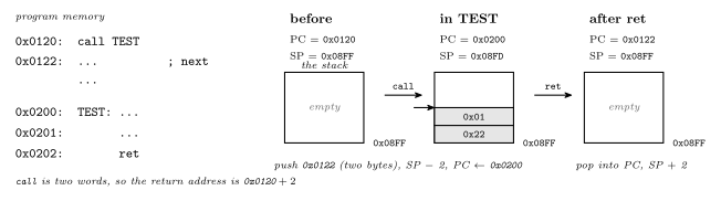
Figure 69: A call and its return, followed through the three registers involved. The PC, the stack pointer and the top of the stack are shown before the call, during the procedure and after the return, with example addresses. call records the address of its own successor on the stack and lowers the stack pointer by two, because a program-memory address needs two bytes; then it loads the PC with the procedure’s address. ret reverses both steps and execution resumes at the recorded address, which is the instruction after the call. The procedure body never touches the return address, so it does not matter what the procedure does in between, provided it leaves the stack as it found it.
Why a stack
The return address has to be stored somewhere. There are three candidates:
| Where | Fails when |
|---|---|
| A single fixed register or memory address for all calls | a procedure calls another procedure — the second call overwrites the first’s return address, and the outer procedure can never return |
| One memory location per procedure | a procedure calls itself — recursion needs two live return addresses for one procedure |
| A stack | never, until memory runs out |
A stack is a last-in, first-out store: push puts a value on top, pop takes the top value off. Calls and returns nest — the most recent call is always the first to return — so a stack of return addresses always has the right one on top. Nested calls are drawn step by step in 2026-09-14-flow-of-control.
The AVR stack
On the AVR the stack is simply a region of data memory (memory-models), and the stack pointer is a 16-bit address held in two I/O registers, SPH:SPL, that says where the top currently is. Two conventions fix how it works:
- The stack grows downward. A push stores at the address in
SPand then decrementsSP; a pop incrementsSPand then loads from it. SoSPalways points at the next free cell, just below the most recently pushed byte. - It starts at the top of SRAM. Program variables are allocated from the bottom of SRAM upward; the stack is started at the last address,
RAMEND(0x08FFon the ATmega324A), and grows down toward them. Neither has to know in advance how much room the other needs.
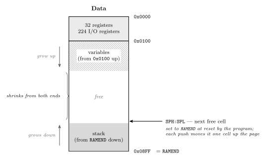
Figure 70: Where the stack lives in the ATmega324A’s data memory. The general-purpose registers and I/O registers occupy the first 256 addresses; SRAM begins at 0x0100. Global variables are laid out from the bottom of SRAM upward, and the stack starts at the top, RAMEND, and grows downward toward them, with SPH:SPL holding the address of the next free cell. The gap between them is the free memory, and it shrinks from both ends: every nested call, every push and every local variable of a running function takes cells off the top, and the stack overflows when it reaches the variables — silently, since nothing checks. That is why the stack pointer must be set to RAMEND before the first call: the reset value would put it somewhere else entirely.
Initialising the stack pointer
An assembly program must initialise the stack before using it. These four lines belong at the top of RESET: in any program that calls anything:
.def temp=r16
    ldi  temp, low(RAMEND)
    out  SPL, temp
    ldi  temp, high(RAMEND)
    out  SPH, temp
RAMEND is defined by the device include file (avr-io-ports), and low()/high() split the 16-bit value because SPL and SPH are two separate 8-bit I/O registers. In C the compiler emits this itself as part of the start-up code that runs before main; it is one of the things a C program on the AVR gets for free and an assembly program does not. The RESET template in avr-program-structure does not include it only because nothing in the Lab 10 programs made a call.
push and pop
The two stack instructions are also available directly:
| Cycles | ||
|---|---|---|
push rr |
store rr at SP, then SP ← SP − 1 |
2 |
pop rd |
SP ← SP + 1, then load rd from SP |
2 |
Their main use is saving registers a procedure is about to clobber, so that the caller gets them back unchanged:
TEST:
    push r16           ; save what the caller had in r16 and r17
    push r17
    ...                ; use r16, r17 freely
    pop  r17           ; restore — in REVERSE order
    pop  r16
    ret
The order matters because the stack is LIFO: the last register pushed is the first one back. And the count matters even more — every push must be matched by a pop before the ret, because ret pops whatever is on top and treats it as the return address. One push too many and the procedure returns to an address made of a register’s contents; one too few and it returns into the middle of the saved data.

Figure 71: Saving and restoring registers around a procedure body, with the stack drawn after each instruction. The return address is already on the stack when the procedure starts; the two pushes go on top of it, and the two pops must come off in the reverse order to land in the right registers. When ret runs the return address is back on top, exactly as call left it. If the pops were in the same order as the pushes, r16 and r17 would come back swapped; if one pop were missing, ret would pop the saved r16 and jump to whatever address that byte pair happened to spell.
Arguments and results
Arguments are passed and results returned in one of two ways: in registers, or on the stack.
- Registers are the fast way for a few small values: the caller puts the argument in an agreed register before the
call, the procedure reads it there and leaves its result in an agreed register for the caller to pick up. Agreement is the whole trick — both sides must use the same register, and a procedure that uses registers for arguments cannot also expect them preserved. - The stack is the general way: the caller pushes the arguments, then calls; the procedure finds them on the stack just above the return address, and results can be returned the same way or in registers. The return address, the arguments and any saved registers and locals together are the procedure’s stack frame. It costs pushes and pops, but it works for any number of arguments and for recursion, since every live call has its own frame.
The AVR C compiler uses both: the first few arguments of a function travel in registers, r24 down, and the rest on the stack, and a function’s local variables live in its stack frame. Those details are the compiler’s convention, and they are why a C function call is not free — see the main costs in c-language-basics.
A C function’s stack frame
A C compiler puts a function’s local variables in its stack frame, next to the return address and any arguments passed on the stack. The frame is pushed when the function is called and popped when it returns. A local therefore exists only while its call is running, and each call, including each level of a recursion, gets its own copy at its own address. An optimising compiler keeps a small local in a register when it can. The frame is where it goes when it needs memory, and the lifetime is the same either way.
In address order, from high to low, which is the order they are pushed:
- arguments, pushed by the caller before the call, if any are passed on the stack;
- the return address, pushed by
call; - locals, made by the function itself when it starts.
A static local is not in the frame. It is stored with the globals, at a fixed address, so it outlives the call and still holds its value the next time the function runs. Globals sit at the bottom of SRAM, the heap grows up above them, and the stack grows down from RAMEND. A stack that grows far enough to meet the heap has overflowed. How the compiler lays out the whole data memory is in compilation-and-linking.
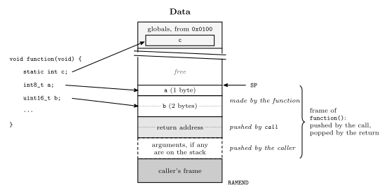
Figure 72: The stack frame of a C function while it runs, with the lowest address at the top as in the course’s memory maps. The caller pushed any stack arguments, call pushed the return address, and the function made room for its locals a and b above that. SP points at the next free cell, just above the frame. When the function returns, the whole frame is popped and SP goes back to where it was before the call, so a and b no longer exist. The static local c is not in the frame at all. It is stored among the globals at a fixed address, which is why it keeps its value from one call to the next.
The stack and interrupts
An interrupt uses the same stack in the same way. The hardware pushes the return address exactly as call would, and the handler’s reti pops it, like ret (avr-interrupts, 2026-09-21-interrupts). Three things follow:
- The stack pointer must be set before interrupts are enabled, not merely before the first
call. An assembly program with no procedures at all still needsSPinitialised once it uses an interrupt. - A handler’s pushes and pops must balance, and it must restore every register it uses. This is the same rule as for a procedure, but stricter: an interrupt can arrive between any two instructions, so there is no caller to agree anything with (polling-and-interrupts).
- Every interrupt that is being handled holds stack space: two bytes of return address plus whatever its handler pushes, and more again if handlers are allowed to nest.
Pitfalls
- Forgetting to initialise
SPin an assembly program. The firstcallpushes to wherever the reset value points; theretthen reads garbage. In C, not a concern. - Unbalanced push/pop inside a procedure — see Figure 71.
retdoes not check what it pops. - Stack overflow. Deep recursion, or big local arrays in C, walk the stack down into the heap and the variables. Nothing on the chip detects it; the symptom is variables changing value for no visible reason.
- Returning a pointer to a local. The local’s frame is popped by the return, so the pointer points at stack space that the next call will reuse.
- Clobbering the caller’s registers. A procedure that uses
r16without saving it changesr16for whoever called it. Either save and restore, or document which registers the procedure destroys — and be consistent.
See also
- avr-branches-and-jumps —
jmp,rjmp,ijmp, and the conditional branches - avr-program-structure — the
RESETtemplate the stack initialisation goes into - memory-models · avr-architecture — data memory,
RAMEND, and the I/O registersSPH/SPL - avr-instructions —
push,pop,call,retamong the rest - c-language-basics — functions in C, which compile to exactly this
- compilation-and-linking — where the compiler puts globals, locals, statics and the heap · 2026-10-15-compilation-and-linking — Lecture 22
- avr-interrupts · polling-and-interrupts — the same stack, used by the hardware
- 2026-09-14-flow-of-control — Lecture 15 · 2026-09-21-interrupts — Lecture 17, the stack under interrupts
Pulse Width Modulation
Pulse width modulation (PWM): making a digital output behave like an adjustable analog one by switching it on and off quickly and controlling what fraction of the time it is on. What the duty cycle is, why a fast pulse train has an average value, what that is good for, and how the AVR’s timer/counters generate it in hardware in their two fast PWM modes. From 2026-09-17-pulse-width-modulation; the timers themselves are in avr-timers-and-counters.
Duty cycle
A PWM signal is a periodic pulse — high for part of each period, low for the rest — and it is described by two numbers:
| Period \(T\) (s), or equivalently the frequency \(f = 1/T\) (Hz) | how often the pulse repeats |
| On-time \(T_{ON}\) (s) | how long the output is high in each period |
\[\text{duty cycle} = \frac{T_{ON}}{T} \times 100\%\]
The duty cycle is the percentage of the time the signal is on (high). 0 % is a constant low, 100 % a constant high, 50 % a square wave; modulating the pulse width means changing \(T_{ON}\) while \(T\) stays fixed. The five duty cycles are drawn in 2026-09-17-pulse-width-modulation.
Average value
If the pulses are fast enough, the signal looks like its average. The average of a periodic voltage is the area under one period divided by the period, and for a pulse between 0 and \(V\) the area is a rectangle:
\[V_{avg} = \frac{1}{T}\int_0^{T} v(t)\,dt = \frac{1}{T}\int_0^{T_{ON}} V\,dt = V \cdot \frac{T_{ON}}{T}\]
so the average voltage is the supply voltage times the duty cycle — 1.25 V at 25 % of 5 V, 2.5 V at 50 %. That is the whole point: a pin that can only ever be at 0 V or 5 V delivers, on average, any voltage between, set by a number in a register.
Fast enough means fast compared with the load. A motor’s inertia, a lamp’s thermal mass, the eye’s persistence or an explicit low-pass filter each smooth the pulses into their average; if the period is long enough for the load to follow the pulses, it sees pulses. So the frequency is chosen for the load once, and the duty cycle is the only thing varied afterwards.
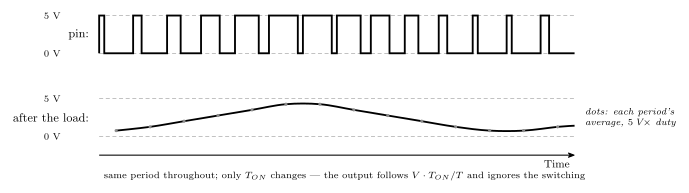
Figure 73: A PWM signal and what a slow load makes of it. Above, the pin’s actual voltage: pulses at a fixed period whose width steps up and then down. Below, the same signal after a low-pass filter — a motor’s inertia, an LED as the eye sees it, or a real RC network before a speaker — which cannot follow individual pulses and settles at their running average. The filtered output tracks the duty cycle and not the pulses, with a small ripple left over from the switching, and moving the duty cycle from period to period moves the output smoothly: an analog waveform out of a digital pin. The higher the PWM frequency relative to the load’s response, the smaller the ripple.
What it is for
Generating signals that look analog from a purely digital source. The AVR has no digital-to-analog converter, and PWM plus the load’s own smoothing is how it gets an analog-looking output:
- Varying the brightness of lights and LEDs — fading is ramping the duty cycle; the eye averages
- Motor control — the average voltage sets the speed of a DC motor; the inertia averages
- Generating audio, with appropriate filtering — vary the width from period to period so the average traces a waveform, filter off the pulses, and what is left is the tone
PWM on the AVR: fast PWM
A timer/counter (avr-timers-and-counters) generates PWM with no software involvement at all. The mechanism is the same in every mode: the count is a sawtooth, a compare register draws a horizontal line across it, and the pin changes state where they cross — once at the match and once more when the count wraps. Moving the compare value moves the crossing along the ramp, which moves one edge of the pulse. That is the modulation.
The waveform generation mode bits pick what the top of the sawtooth is, and the compare output mode bits pick which way the pin switches at the crossing.
Mode 3 — top fixed at 255 (WGM[2:0] = 011)
The count runs 0 to 255 and wraps: every period is exactly 256 ticks, so
\[T_{tick} = \frac{1}{CLK/PRE} \qquad T = \frac{256}{CLK/PRE} \qquad f = \frac{CLK}{256 \cdot PRE}\]
and the frequency is set entirely by the prescaler. Both compare registers are free to make pulses, so one timer gives two independent PWM outputs at the same frequency, OCnA and OCnB. With the compare value at 191 the pin is high for 64 of the 256 ticks in inverting mode, a 25 % duty cycle — the worked example in 2026-09-17-pulse-width-modulation.
Mode 7 — top in OCRnA (WGM[2:0] = 111)
The count wraps when it reaches OCRnA instead of 255: the period is OCRnA + 1 ticks and can be chosen,
\[T = \frac{1 + OCRnA}{CLK/PRE} \qquad f = \frac{CLK}{(1 + OCRnA) \cdot PRE}\]
The pulse is then made on the other compare unit, OCRnB against the shorter ramp. The price of choosing the frequency is that compare unit A is spent on it: one PWM output per timer, and OCnA can at most toggle on each wrap. With OCRnA = 127 and OCRnB = 95 the period is 128 ticks and the inverting output is high for 32 of them — again 25 %.
Both are cases of the master formula \(f = CLK / (PRE \cdot (TOP + 1))\) with \(TOP = 255\) or \(TOP = OCRnA\).
Inverting and non-inverting
The compare output mode bits COMnx1:0 decide what the crossing does to the pin in fast PWM:
COMnx1:0 |
On compare match | At the wrap (BOTTOM) | Pulse is high for | Duty cycle |
|---|---|---|---|---|
10 — non-inverting |
clear OCnx |
set OCnx |
OCRnx + 1 ticks, from the wrap to the match |
\(\dfrac{OCRnx + 1}{TOP + 1}\) |
11 — inverting |
set OCnx |
clear OCnx |
\(TOP - OCRnx\) ticks, from the match to the wrap | \(\dfrac{TOP - OCRnx}{TOP + 1}\) |
01 |
toggle OCnA — mode 7 only, and only unit A |
a square wave at half the wrap rate | 50 % | |
00 |
pin disconnected — ordinary port pin |
The two outputs are complements: the same crossing, opposite polarity, and their on-times add to a full period. Non-inverting is the natural choice — a bigger number means a wider pulse — and is what duty cycle = (OCR + 1) / 256 refers to.
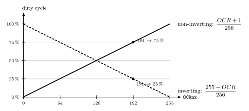
Figure 74: How the compare value maps to duty cycle in mode 3, for the two polarities. In non-inverting mode the pulse runs from the wrap to the match, so it is \(OCR + 1\) ticks of 256 and the duty rises linearly with the register from just under 0.4,% at 0 to 100,% at 255. In inverting mode the pulse runs from the match to the wrap, so it is \(255 - OCR\) ticks: the same line reflected, 100,% at 0 down to 0,% at 255. The two always sum to 100,%. Neither polarity reaches both ends: non-inverting cannot give a true 0,% (a compare value of 0 still gives one tick high) and inverting cannot give 100,%; a program that needs the output fully off disconnects the pin instead.
Setting it up
Four registers, all from the header names (c-preprocessor-and-avr-headers, bit-masking) — timer 0, mode 3, non-inverting on OC0B (PB4), clock ÷ 64, 25 % duty:
DDRB   |= (1<<4);                              /* OC0B is PB4: the timer decides what, DDR decides whether */
TCCR0A  = (1<<COM0B1) | (1<<WGM01) | (1<<WGM00); /* non-inverting on B; fast PWM, TOP = 255 */
TCCR0B  = (1<<CS01) | (1<<CS00);               /* clock / 64: 8 MHz / (256 * 64) = 488 Hz */
OCR0B   = 63;                                  /* (63 + 1) / 256 = 25 % */
After this the CPU never touches the pin; changing the duty cycle is one assignment to OCR0B, and it takes effect at the next wrap. The compare registers are double buffered in the PWM modes: a value written is held back and loaded when the count wraps, so a pulse already under way is never cut short. The frequencies mode 3 can produce at 8 MHz are one per prescaler tap:
| Prescaler | \(f = 8\,\text{MHz} / (256 \cdot N)\) |
|---|---|
| 1 | 31.25 kHz |
| 8 | 3.91 kHz |
| 64 | 488 Hz |
| 256 | 122 Hz |
| 1024 | 30.5 Hz |
For an LED anything from 122 Hz up is flicker-free; for audio the 31.25 kHz setting is the one above hearing. If a frequency between the taps is needed, mode 7 with an OCR0A chosen from the master formula.
Phase correct PWM
The other family of PWM modes has the counter count up and then down — a triangle rather than a sawtooth — and switch the pin at the compare value on both slopes. The pulse is then symmetric about the peak of the triangle, so the centre of every pulse stays at the same point in the period as the width changes, instead of the leading edge staying fixed and only the trailing edge moving. That is smoother for motor control, where the timing of the current pulse relative to the period matters; the cost is a period twice as long for the same top, so half the frequency. Timer 1 adds a phase and frequency correct variant on top. The two families are drawn side by side in 2026-09-17-pulse-width-modulation. This course uses fast PWM only.
See also
- avr-timers-and-counters — the timers: registers, clock select, prescaler, modes, the master formula
- week8-lab-avr-timers — Lab 12:
WGM,CSandCOMbit by bit; the formula worked for a toggling pin - week9-lab-avr-pwm — Lab 13: two LEDs faded on timer 0, and a tone of adjustable pitch and duty cycle on timer 1
- 2026-09-17-pulse-width-modulation — Lecture 16 · 2026-09-14-flow-of-control — Lecture 15
- avr-io-ports — the
DDRbit the timer still needs · timing-diagrams — how the waveforms are drawn
Seven-Segment Display
How a digit is shown on the IO board’s seven-segment display: the segment lettering, the byte that lights a pattern, the lookup table for all ten digits, and the common-cathode line that selects which of the two digits is lit. First met in 2026-09-10-more-c-programming-on-the-avr; the board’s header is in io-board and the port registers in avr-io-ports.
Segments
Seven bars lettered a to g, plus a decimal point dp:
| Segment | Position |
|---|---|
| a | top |
| b | upper right |
| c | lower right |
| d | bottom |
| e | lower left |
| f | upper left |
| g | middle |
| dp | the dot, lower right |
— clockwise from the top for a to f, then g across the middle. Each segment is an LED; a 1 on its line lights it.
The byte
The display is driven from one 8-bit port, one bit per segment, in this order:
| bit 7 | bit 6 | bit 5 | bit 4 | bit 3 | bit 2 | bit 1 | bit 0 |
|---|---|---|---|---|---|---|---|
| dp | g | f | e | d | c | b | a |
So the byte for a digit is read off by asking, segment by segment, whether it is lit. Two worked examples:
| Digit | Lit | dp g f e d c b a | Sum | Decimal |
|---|---|---|---|---|
| 0 | a b c d e f | 0 0 1 1 1 1 1 1 |
\(32 + 16 + 15\) | 63 |
| 2 | a b g e d | 0 1 0 1 1 0 1 1 |
\(64 + 16 + 8 + 3\) | 91 |
PORTA = 63; shows a 0; PORTA = 91; shows a 2. The 2 and both bytes are drawn in 2026-09-10-more-c-programming-on-the-avr.
All ten digits
The lookup table from the program below, decoded:
| Digit | Decimal | Binary (dp g f e d c b a) | Segments lit |
|---|---|---|---|
| 0 | 63 | 0011 1111 |
a b c d e f |
| 1 | 6 | 0000 0110 |
b c |
| 2 | 91 | 0101 1011 |
a b d e g |
| 3 | 79 | 0100 1111 |
a b c d g |
| 4 | 102 | 0110 0110 |
b c f g |
| 5 | 109 | 0110 1101 |
a c d f g |
| 6 | 125 | 0111 1101 |
a c d e f g |
| 7 | 7 | 0000 0111 |
a b c |
| 8 | 127 | 0111 1111 |
a b c d e f g |
| 9 | 111 | 0110 1111 |
a b c d f g |
Displays differ on whether 6 lights segment a, the top bar, and whether 9 lights segment d, the bottom bar. This table lights both, giving a hooked 6 and an underlined 9.
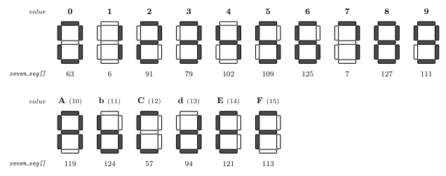
Figure 75: All sixteen values a nibble can hold, as seven-segment patterns, with the byte that produces each one in decimal underneath — the sixteen entries of the lookup table in order. Heavy segments are lit; the bit order is dp g f e d c b a with a at bit 0, so each number is read straight off the lit segments: 63 is every segment but g, 6 is b and c alone. The hex letters b and d are lowercase because their capitals would be indistinguishable from 8 and 0 on seven segments; A, C, E and F have no such clash.
Hex digits A–F
Four input bits hold 0–15, and the six values past 9 can be shown too, as hex letters. Two of them have to be lowercase: an uppercase B on seven segments is an 8, and an uppercase D is a 0.
| Value | Shows | Segments lit | dp g f e d c b a |
Decimal |
|---|---|---|---|---|
| 10 | A | a b c e f g | 0111 0111 |
119 |
| 11 | b | c d e f g | 0111 1100 |
124 |
| 12 | C | a d e f | 0011 1001 |
57 |
| 13 | d | b c d e g | 0101 1110 |
94 |
| 14 | E | a d e f g | 0111 1001 |
121 |
| 15 | F | a e f g | 0111 0001 |
113 |
With these appended the table has sixteen entries and every value a masked nibble can produce is a valid index, so the guard in the program below can go:
uint8_t seven_seg[16] = { 63,6,91,79,102,109,125,7,127,111,
                          119,124,57,94,121,113 };
This is Lab 11’s Task 2 (week8-lab-avr-c-programming), and the same table drives the hex adder of its Task 3.
The program
#include <avr/io.h>

/* Seven segment display values */
uint8_t seven_seg[10] = { 63,6,91,79,102,109,125,7,127,111};

int main(void) {
  uint8_t digit;

  /* Set port A pins to be outputs, port C pins to be inputs */
  DDRA = 0xFF;
  DDRC = 0;    /* This is the default, could omit. */
  while(1) {
    /* Read in a digit from lower half of port C pins */
    /* We read the whole byte and mask out upper bits */
    digit = PINC & 0x0F;
    /* Write out seven segment display value to port A */
    if(digit < 10) {
      PORTA = seven_seg[digit];
    } else {
      PORTA = 0;
    }
  }
}
Port A drives the eight segment lines; the low four bits of port C are the input digit. The loop reads the digit, masks off the upper nibble (bit-masking), looks the pattern up and writes it. The if guards the table — four bits can be 10–15, and seven_seg[10] is past the end of the array (c-pointers-and-arrays); those inputs blank the display instead.
Lookup table, not arithmetic. There is no formula that turns a digit into its segment pattern, so the program does not try: the ten answers are precomputed and indexed. It is the general pattern for any input-to-output mapping that is small and irregular, and it is what the array is for.
Two digits, one set of lines: CC
On the IO board the display has two digits but the header carries one set of segment pins — DP, G … A — plus one more, CC, the common cathode (io-board). The segment lines go to both digits; CC decides which one is actually lit:
CC |
Lit |
|---|---|
| 1 | left digit |
| 0 | right digit |
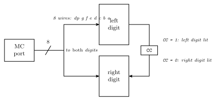
Figure 76: Why one port can drive two digits. The eight segment lines are wired to both digits in parallel, so both always receive the same pattern; the CC line selects which digit’s common cathode is connected to ground, and only that digit lights. One byte and one select bit therefore describe the whole display at any instant. To show two different digits the program alternates — left pattern with CC = 1, then right pattern with CC = 0 — fast enough that the eye sees both at once.
Writing a digit therefore takes two outputs: the segment byte on port A, and CC on whichever pin it is wired to. The program above drives a single digit and never touches CC; in Lab 11 CC is simply jumpered to a button, so pressing it moves the same digit across.
Display multiplexing
Showing a two-digit number means time-sharing the segment lines: write the tens pattern with CC = 1, wait, write the ones pattern with CC = 0, wait, repeat. Alternate fast enough — every millisecond, say — and persistence of vision merges the two into a steady two-digit display, each digit at half brightness because it is lit half the time. Slow the alternation to a few times a second and the trick becomes visible, with the digits taking turns. The waiting is a timer’s job (avr-timers-and-counters); the whole program, and a timing diagram of the two digits taking turns, is Lab 12’s Task 2 (week8-lab-avr-timers). Two things the ordering has to get right: write the segments before switching CC, so the newly selected digit never flashes the other digit’s pattern, and keep the tick regular, or one digit will look brighter than the other.
See also
- io-board — the header pins
CC DP G F E D C B A, and where the display sits on the board - avr-io-ports —
DDRA,PORTA,PINC - bit-masking —
PINC & 0x0F - c-pointers-and-arrays — the lookup table
- c-preprocessor-and-avr-headers — why
PORTAcan be assigned to - 2026-09-10-more-c-programming-on-the-avr — Lecture 14
- week8-lab-avr-c-programming — Lab 11: the display wired up, hex digits, the adder · week8-lab-avr-timers — Lab 12: display multiplexing on a timer tick · week9-lab-avr-interrupts — Lab 14: the display as a stopwatch
Timing Diagrams
A timing diagram is the fourth of the four equivalent ways to describe a logic function, alongside the logic diagram, the truth table, and the Boolean expression (see logic-gates).
Timing diagram as a logic representation
It is like a truth table, but in graphical format: time runs left to right along the horizontal axis, and each signal gets its own horizontal track that steps between the logic 0 and logic 1 levels (drawn as two dashed reference lines).
Worked example — an inverter. The input waveform starts at logic 0, rises to logic 1 for a period, then falls back to logic 0. The output waveform is the mirror image: it starts at logic 1, falls to logic 0 for exactly that period, then returns to logic 1. Each change in the input causes the output to change.
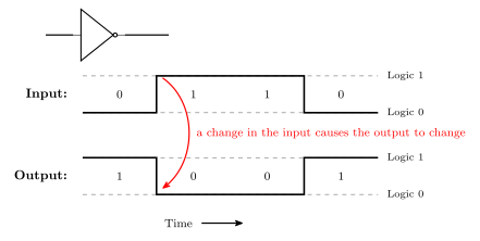
Figure 77: An inverter drawn as a timing diagram. Reading the four intervals off the input gives 0, 1, 1, 0 and off the output gives 1, 0, 0, 1 — which is the inverter’s truth table, just laid out along a time axis instead of down a page. The two dashed lines per track are the logic 0 and logic 1 reference levels.
At this idealised level the output changes at exactly the same instant as the input; the transitions are drawn as vertical lines. That is a convenient fiction, corrected at the bottom of this note.
Convention for drawing the input waveforms
The input waveforms must be drawn so that all possible input combinations are covered — that is what makes the diagram equivalent to the full truth table.
The standard construction for a 2-input gate divides the time axis into four equal intervals and drives the inputs like a binary count:
- \(A\) is low for the first half of the diagram, then high for the second half.
- \(B\) toggles at twice that rate: low, high, low, high.
Reading the four intervals left to right therefore gives \(AB = 00, 01, 10, 11\) — every combination, once each, in truth-table order. For \(n\) inputs the same scheme generalises: input \(i\) toggles at half the rate of input \(i+1\), and the diagram is \(2^n\) intervals wide.
To read a gate’s output off the diagram, work interval by interval: identify the \(AB\) combination in that interval, look up the gate’s truth table row, and draw the output at that level for the width of the interval.
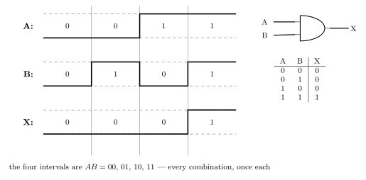
Figure 78: The convention on a 2-input example, with the AND output filled in. The vertical rules divide the four intervals; the digits under each track are the truth-table row for that interval. Because the inputs count 00, 01, 10, 11, the output track is literally the output column of the truth table, drawn left to right.
Going the other way — being given the output track and asked which gate it is — is the standard exam form of this. Read the output value in each interval, write it beside the corresponding \(AB\) row, and compare the resulting column with the gates you know. A worked instance is in 2026-08-06-combinational-logic.
Real gates aren’t perfect: the reality of timing
The idealised diagrams above show instantaneous, perfectly square transitions. Real gates do not behave that way — real waveforms have sloped edges, and the output changes some time after the input does. Three quantities describe this:
| Term | Definition |
|---|---|
| Propagation delay | Time for a change in the input to affect the output. |
| Fall time | Time taken for the output to fall from 1 to 0. |
| Rise time | Time for the output to rise from 0 to 1. |
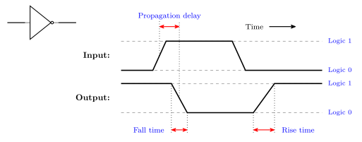
Figure 79: The same inverter drawn honestly. The input’s edges slope instead of jumping; the output does not begin to move until the propagation delay has elapsed; and once moving, its downward edge takes the fall time and its later upward edge takes the rise time. Rise and fall times are properties of one edge of one signal — the propagation delay is the gap between two signals.
Measured on an inverter: the input ramps up, and only after the propagation delay does the output begin to move; the output’s downward edge then takes the fall time to complete, and its later upward edge takes the rise time.
The three quantities are measured differently, and it is worth keeping them apart. Rise time and fall time are properties of a single edge of a single waveform — how long that edge takes to get from one level to the other. Propagation delay is the gap between two waveforms — how long the output takes to react at all. All three are marked on the same pair of inverter waveforms above.
Comments and directives
Comments start with semicolons. Everything from a
;to the end of the line is ignored by the assembler..include "m324Adef.inc"is an assembler directive, not an instruction — nothing is generated for it. The contents of the file are included directly in the program, which is what makesDDRA,PORTC,TCNT0and the rest usable as names instead of I/O register numbers (see avr-io-ports). The leading dot is the giveaway: a line starting.speaks to the assembler, a line starting with a mnemonic speaks to the CPU.Every line has the same shape, with up to four fields: a label, an operation, its operands and a comment, as in
loop: jmp loop ; Repeat. The operation is either an instruction or, with the leading dot, a directive. Two more directives turn up in most programs:.def temp = r16gives a register a name, and.equgives a number a name. The fields, and every directive with what it does, are in assembly-process.