Lecture 11 — Instruction Set Architecture Part 1
The ISA is a document, and this is what is in the document. See instruction-set-architecture for the four-part frame, memory-models for the first part in full, avr-architecture for the register file and avr-io-ports for the I/O registers.
The ISA as an interface
Machine code, the ISA as a specification, and a first look at the AVR are in 2026-08-27-avr-introduction. The split between specification and implementation, in the form the rest of the course leans on:
- The ISA defines the interface between hardware and software. The ISA is a specification; the microarchitecture is how the control unit is built.
- Hardware (microarchitecture) designers don’t need to know about the high level software. They just build a microarchitecture that implements the ISA.
- Software writers (machine language programmers and compiler writers) don’t need to know (much) about microarchitecture. They just write or generate instructions that match the ISA.
Picture software (SW) above, hardware (HW) below, and on the line between them a row of bits — 1 0 1 0 1. The interface is not an API or a protocol; it is a bit pattern, and both sides are built from the same document that says what the pattern means.
What makes an ISA?
Four things:
- Memory models
- Registers
- Instructions
- Data types
Parts 1 and 2 and the start of part 3 are below. Instructions continue and data types arrive in 2026-09-03-instruction-set-architecture-part-2. The payoff: if you know all these details you can write machine code that runs on the CPU, and build the CPU.
1. Memory models
The memory model is how memory looks to the CPU. There are four issues, better read as decisions the specification has to make than as problems to be solved:
- A. Addressable cell size
- B. Alignment
- C. Address spaces
- D. Endianness
Full treatment in memory-models.
Memory organisation
Computer memory is conceptually a set of addressable cells. Cells are usually 8 bits wide (one byte), though various cell widths have been used in the past. Drawn as a grid, the address indexes down the left and the cell width runs across.
Take a 4 × 3 memory: 4 addresses, 3-bit cells. \(2^2 = 4\), so two address bits name four cells.
At gate level that memory is built like this:
- One cell is a row of three D flip-flops.
- The address decoder turns
A1 A0into one row-select line.A1 A0 = 0 1selects row 1. WRITE= 1 gatesDATA IN(I2 I1 I0) into the selected row through the AND gates on the left. The selected row’s outputs reachDATA OUT(O2 O1 O0) through the AND-OR tree on the right.
Nothing new appears here: it is flip-flops-and-latches for the storage and combinational-logic-blocks for the selection. Memory is a decoder, some flip-flops and some gates. The whole schematic is in memory-models.
A. Addressable cell size
The most common cell size is 8 bits (1 byte), but not always. The AVR is the counterexample:
| AVR | Cell width |
|---|---|
| data | 8 bits |
| program | 16 bits |
The bus is used to transport the content of a cell. Sometimes the data bus is wider than a cell, i.e. it retrieves several cells (addresses) at once, and then the address bus does not need to be as wide.
Bus sizes
For every doubling of data bus width, remove the least significant bit of the address bus.
For \(2^n\) cells of 8 bits, the address size is \(n\) bits, and the configurations are:
| Data bus | Address bus | Transferred |
|---|---|---|
| 8 bits | \(n\) | one cell at a time |
| 16 bits | \(n-1\) | two cells at a time |
| 32 bits | \(n-2\) | four cells at a time |
A concrete case: a memory with addresses 000000, 000001, 000010, … up to 111111, each cell 8 bits wide.
\[64 \text{ cells} = 2^6 \implies 6 \text{ address bits}\]
Group the cells in pairs and then in fours, and the address bus A goes 6, 5, 4 bits as the data bus D goes 8, 16, 32.
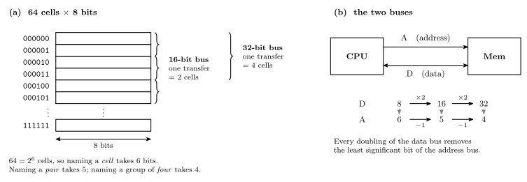
Figure 1: The bus-width trade-off. (a) 64 cells of 8 bits, so a cell needs a 6-bit address. A 16-bit data bus can only ever hand over an aligned pair of cells, and there are 32 pairs — 5 bits; a 32-bit bus hands over a group of four, and there are 16 groups — 4 bits. (b) the same fact read off the two buses at once: every doubling of D removes one bit from A.
Widening the data bus by a factor of two narrows the address bus by exactly one bit, because the transfer now names a group of cells rather than a cell.
Worked: address bus width
If a CPU supports \(2^{35}\) bytes of memory and has a 64 bit data bus, how many bits wide is the address bus?
32.
Start from the cell size. Cell = 8 bits, so \(2^{35}\) bytes is \(2^{35}\) cells, and a byte-at-a-time machine would need a 35-bit address. Then walk the ladder, doubling the data bus and dropping one address bit each time:
| Data bus | 8 | 16 | 32 | 64 |
|---|---|---|---|---|
| Address bus | 35 | 34 | 33 | 32 |
Three doublings from 8 to 64, so three bits off 35.
B. Alignment
Many architectures require natural alignment, e.g. 4-byte words starting at addresses 0, 4, 8, … and 8-byte words starting at 0, 8, 16, …
An 8-byte example, counting the reads:
| Reads | ||
|---|---|---|
| aligned — 8-byte word at address 8 | occupies exactly the block 8–15 | one |
| non-aligned — 8-byte word at address 12 | half in block 8–15, half in block 16–23 | two |
Alignment is often required because it is more efficient. The counter-example is the Pentium IV, which fetches 8 bytes at a time from memory (64-bit wide data bus) and for which alignment is not required, so the processor stays backwards compatible with earlier processors:
- a 4-byte word stored at address 4 takes 1 read (bytes 0 to 7);
- a 4-byte word stored at address 6 must read bytes 0 to 7 (one read) and bytes 8 to 15 (second read), then extract the 4 required bytes from the 16 bytes read.
Worked: counting reads
How many memory reads are needed to read an 8-byte value on a machine with a 16-bit data bus that does not require natural alignment?
4 or 5.
There are two cases, an even start address and an odd one:
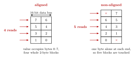
Figure 2: Reading an 8-byte value on a 16-bit data bus. Each row is one 2-byte block, i.e. one read; the numbers are the eight bytes of the value. Start the value at an even address and it fills four whole blocks — 4 reads. Start it at an odd address and one byte sits alone in the block at each end, so five blocks have to be read for eight bytes. Addresses increase upward and the higher-addressed byte of each block is drawn on the left. A × marks a byte in the fetched block that is not part of the value (csse2010-diagram-notation).
“Does not require” is the operative phrase — the machine permits both, so the answer has to cover both. That is why every question of this shape answers “\(k\) or \(k+1\)” rather than a single number.
C. Address spaces
Many microprocessors have a single linear memory address space — the von Neumann architecture — e.g. \(2^{32}\) bytes numbered from 0 to \(2^{32} - 1\) (which may not be bytes — it depends on the addressable cell size). Picture one strip with data at the low end and program at the high end: one space, shared.
The Harvard architecture has separate address spaces for instructions and data: two spaces, each starting at its own 0.
The AVR ATmega 324A is Harvard:
| Size | ||
|---|---|---|
| Data address space | \(2^{11}\) (2048) bytes | 2 kB, 8-bit cells |
| Instruction address space | \(2^{14}\) 16-bit words | 16,384 instruction words = 32,768 bytes |
The working:
\[2 \cdot 2^{10}\,\text{B} \to 2^{11} \text{ cells} \to 11 \text{ bits}\] \[2^{5} \cdot 2^{10}\,\text{B} = 2^{15}\,\text{B} \xrightarrow{\ \div 2\ } 2^{14} \text{ cells} \to 14 \text{ bits}\]
The \(\div 2\) is the step people drop. 32 kB of program memory is \(2^{15}\) bytes but only \(2^{14}\) addresses, because each address names a 16-bit cell. Convert to cells first, then take the logarithm.
The datasheet memory map fills that in — 32 registers, 64 I/O registers, 160 extended I/O registers and then 2 kB of SRAM up to 0x08FF on the data side; 0x0000 to 0x3FFF of Application and Boot flash on the program side. The map is in memory-models; the rest of the chip is in avr-architecture.
The \(2^{11}\) bytes is the size of the SRAM only. The data space itself runs to 0x08FF, which is that 2 kB plus the 256 locations (0x0000–0x00FF) the register file and the I/O registers occupy in front of it. The two I/O bands together hold 224 I/O registers, a number that comes back with the I/O registers below.
D. Endianness
Different machines may support different byte orderings.
| Which end goes at the lowest address | Who | |
|---|---|---|
| Little endian | the little end — least significant byte stored first | Intel microprocessors (Pentium etc.), AVR |
| Big endian | the big end stored first | SPARC, Freescale (formerly Motorola) microprocessors |
Most desktop/workstation/server CPUs produced since ~1992 are bi-endian (support both). Some are switchable at boot time, others at run time, i.e. can change dynamically.
Think of a read as SOURCE → TARGET: four memory cells at addresses \(m\), \(m+1\), \(m+2\), \(m+3\) are the source, a four-byte register is the target, and the bytes either cross over (little endian) or run straight across (big endian).
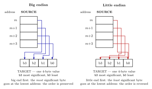
Figure 3: Assembling one 4-byte value out of four memory cells. The only difference between the two machines is which end of the value the lowest address holds. Big endian keeps the order (address \(m\) supplies the most significant byte); little endian reverses it. Nothing about the memory changes — the same four cells give two different values, and only the ISA says which.
Worked example
Given the memory:
| Address | Contents |
|---|---|
| 0 | 00001111 |
| 1 | 00110011 |
| 2 | 11011101 |
| 3 | 00101100 |
The 1-byte word at address 1 is 00110011 — one cell, so endianness does not enter into it.
The 2-byte word at address 0 on a big endian system is 00001111 00110011. Big end first, so address 0 holds the most significant byte and address 1 the least — the arrows run straight across.
Worked: the little endian read
With the memory above, what is the value of the 2-byte word at address 2 if this is a little endian system?
00101100 11011101.
Little end first, so address 2 (11011101) is the least significant byte and address 3 (00101100) the most — and writing the value out most-significant-first therefore reverses them.
There are two mistakes to make here, and only one of them is about endianness. Crossing them gives four candidate answers:
| Which word, read which way | ||
|---|---|---|
| A | 00110011 11011101 |
the word at address 1, read big-endian |
| B | 11011101 00110011 |
the word at address 1, read little-endian |
| C | 11011101 00101100 |
the right word, read big-endian |
| D | 00101100 11011101 |
✓ the right word, read little-endian |
So C is the endianness trap; A and B are the off-by-one trap, both dragging in 00110011 from address 1, which is not part of this word at all.
The reliable procedure: list the addresses the value occupies in increasing order, then assemble the answer most significant byte first. Big endian reads that list forwards, little endian backwards.
2. Registers
There are two types of register:
- General purpose — used for temporary results etc. On the AVR these are r0 … r31.
- Special purpose, e.g. Program Counter (PC), Stack pointer (SP), Input/Output Registers (224 on the AVR), Status Register (flags N Z C V; Tanenbaum calls this the Program Status Word).
Some other registers are part of the microarchitecture, not the ISA — e.g. the Instruction Register (IR). The programmer doesn’t need to know about these, and can’t directly change or use them.
That is the line the ISA draws. The IR exists, holds the instruction, and is in the CPU diagram of avr-architecture — but no instruction names it, so it is not in the specification and a chip designer may do as they like with it. The PC is in the specification because jmp writes it.
AVR registers
The general purpose registers (0–31) are quite regular and can be used interchangeably, with two exceptions:
- A few instructions work on half the registers (registers 16–31). Only 4 bits are used to represent the operand in the instruction, and \(2^4 = 16\). This is the same fact that restricts
LDI, seen from the encoding side (avr-instructions). - The X, Y, Z registers, below.
There are also many I/O registers (224). They are not to be confused with the general purpose registers: some instructions work with I/O registers, others with general purpose registers.
X, Y and Z
The top six registers of the register file pair off into three pointers, listed here with their register addresses:
| Pointer | Pair | Register addresses |
|---|---|---|
| X | R27 : R26 | 0x1B : 0x1A |
| Y | R29 : R28 | 0x1D : 0x1C |
| Z | R31 : R30 | 0x1F : 0x1E |
So Z ≡ R31 : R30. Two 8-bit registers side by side make a 16-bit address, which is what a data space wider than 256 bytes needs and no single register can hold. See avr-architecture.
AVR I/O registers
The AVR ATmega324A has 224 I/O register addresses, used to control peripherals and get data to/from them:
- Timers and counters
- Analog to digital converters
- Serial input/output
- General purpose input/output ports
- Each port (x = A, B, C or D) has three registers: DDRx (data direction register), PORTx (values to output), PINx (values on the pins). See learning lab 11.
Some addresses are reserved (not actually available on this device). Everything about these is in avr-io-ports — and the three port registers turn up a lab early, in week6-lab-avr-io-ports.
3. Instructions
Instructions are the main feature of an ISA. Instruction types include:
| Input/Output | communicate with I/O devices |
| Load/Store | move data from/to memory |
| Move | copy data between registers |
| Arithmetic | addition, subtraction, … |
| Logical | Boolean operations |
| Branching | for deciding which instruction to perform next |
The instructions met so far: MOV rd, rr (copy, not move), ADD rd, rr, AND/OR/EOR rd, rr, and LDI rd, K for r16–r31 (avr-instructions).
Input/output instructions
The 224 I/O registers split into two classes by how you are allowed to reach them:
| Where | Reached by | |
|---|---|---|
| I/O registers 0 to 223 | data memory addresses 32 to 255 ($20 to $FF) |
load and store instructions |
| First 64 (0 to 63) — special | also in and out |
|
| Other 160 (64 to 223) — “extended” I/O registers | load and store only |
Data memory, lowest addresses first, is r0 … r31, then the 64 I/O registers, then the 160 extended I/O registers. That is where the $20 offset comes from: the register file is in the way.
IN and OUT
in rd, P |
Load I/O register value into general purpose register | rd: r0 to r31; P = I/O register number (0 to 63, 0 to 0x3F) |
out P, rr |
Store value from general purpose register into I/O register | rr: r0 to r31; P = 0 to 63 (0 to 0x3F) |
One example of each:
\[\texttt{IN r0, 0} \;\equiv\; \texttt{IN r0, PINA}\] \[\texttt{OUT 1, r0} \;\equiv\; \texttt{OUT DDRA, r0}\]
Picture the CPU holding r0 … r31 on one side and the 64 I/O registers on the other. IN is a read of an I/O register and OUT is a write to one. avr-io-ports draws the pair with one arrow each way.
Two things to take from those two lines. The number and the name are the same operand — I/O register 0 is PINA and I/O register 1 is DDRA, and the name only exists because m324Adef.inc was included. And the destination is written first in both, which is why the I/O register moves from second operand to first between them. Both instructions are one word and one clock cycle. Full detail in avr-io-ports.
Summary
The four parts of an ISA:
- Memory models ✓
- Registers ✓
- Instructions — more in Lecture 12
- Data types — Lecture 12
If you know all these details, you can write machine code that runs on the CPU and build the CPU.
See also
- memory-models — cell size, alignment, address spaces, endianness in full
- instruction-set-architecture · avr-architecture · avr-io-ports · avr-instructions
- flip-flops-and-latches · combinational-logic-blocks — what the 4 × 3 memory is built from
- 2026-08-27-avr-introduction — Lecture 10
- 2026-09-03-instruction-set-architecture-part-2 — Lecture 12
- week6-lab-avr-io-ports — Lab 10, where
inandoutget used