AVR Architecture
The Atmel AVR: what is on the chip, how the CPU is laid out, and where the fetch-decode-execute cycle happens in it. See cpu-organisation for the generic picture this specialises and avr-instructions for what it executes.
Microcontroller, not microprocessor
Atmel AVR devices are microcontrollers. A microcontroller includes lots of components on one chip:
- CPU
- Memory (RAM)
- Program memory
- Input/output devices
That is the distinction from a microprocessor, which is the CPU alone. An ATmega324A is not a CPU — it contains a CPU, alongside memory and a large collection of peripherals, so that a useful system can be one chip rather than a board full of them.
The AVR CPU
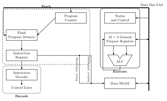
Figure 1: The AVR CPU core, with the three stages of the cycle marked. Fetch (dashed) reads the next instruction from flash under the program counter into the instruction register; decode (dotted) turns it into control lines; execute (solid) runs it over the register file, ALU and status register, with the 8-bit data bus tying everything together. The two lines dropping to the Data SRAM are the direct and indirect addressing routes — both come out of the instruction, which is why they leave from the instruction register. The execute group takes in the status register, the register file and the ALU; the Data SRAM sits outside it.
Reading the diagram as the cycle of fetch-decode-execute-cycle:
| Stage | Blocks involved |
|---|---|
| Fetch | Program Counter → Flash Program Memory → Instruction Register |
| Decode | Instruction Register → Instruction Decoder → Control Lines |
| Execute | General purpose registers → ALU → back to registers, with Status and Control updated |
Because these three groups are largely separate hardware, the AVR overlaps them: while one instruction executes, the next is being fetched. This course calls it a three-stage pipeline. The ATmega164A/324A/644A/1284P datasheet describes the core as “single level pipelining”, i.e. fetch and execute overlapping, which is two stages. Answer three-stage pipeline in the exam, but the datasheet is the authority on the hardware.
The pieces
| Block | Notes |
|---|---|
| Flash program memory | Holds the program. 32 kB on the ATmega324A, and non-volatile — it survives power loss |
| Program Counter | Addresses flash to select the next instruction — the PC of cpu-organisation |
| Instruction Register | Holds the instruction currently being worked on |
| Instruction Decoder | Turns the instruction’s bits into control lines — this is the control unit |
| 32 × 8 general purpose registers | R0–R31, each 8 bits wide, built from flip-flops |
| ALU | 8-bit, so AVR is an 8-bit machine |
| Status and Control | Holds the flags the ALU produces — N, Z, C, V among others |
| Data SRAM | 2 kB, volatile — static RAM, i.e. flip-flops |
| Data bus | 8 bits wide, tying the execute-side blocks together |
Two addressing routes reach the SRAM, drawn as the two vertical paths in Figure 1 — direct addressing (the address is in the instruction) and indirect addressing (the address is in a register). Both leave from the instruction register, because in either case it is the instruction that says which cell is wanted; they differ only in whether it says so with a literal address or with the name of a pointer. Both, and the other two modes, are in addressing-modes.
Four numbers define the chip: the flash is 32 kB and non-volatile; the SRAM is 2 kB, volatile, and made of static flip-flops; the register file is 32 registers, r0…r31, each 8 bits wide and made of flip-flops; and the ALU is 8-bit, which makes the AVR an 8-bit machine.
The register file
General purpose registers (0–31) are quite regular and can be used interchangeably. Two exceptions are worth having by heart:
- A few instructions work on half the registers (r16–r31), because only 4 bits are used to represent the operand in the instruction and \(2^4 = 16\).
LDI,SER,ANDI,ORIandCPIare among them — see avr-instructions. - X, Y and Z are register pairs that double as 16-bit pointers.
X, Y and Z
The top six registers of the file are those three pairs, low byte in the lower-numbered register:
| Pointer | High : Low | Register addresses |
|---|---|---|
| X | R27 : R26 | 0x1B : 0x1A |
| Y | R29 : R28 | 0x1D : 0x1C |
| Z | R31 : R30 | 0x1F : 0x1E |
Two 8-bit registers side by side make a 16-bit address — which is what the data space needs and no single 8-bit register can hold. They are what indirect addressing uses: ld r5, X means “load from wherever X points”, and the instruction only has to name which pointer, so it stays one word (addressing-modes).
The low byte living in the lower-numbered register is the same little-endian convention the AVR uses in memory (memory-models).
Address spaces
The AVR is a Harvard machine — separate address spaces for instructions and data — so 0x0000 names two entirely different locations depending on which space is meant, and the instruction decides.
Data address space — 0x0000 to 0x08FF
| Region | Addresses | Size |
|---|---|---|
| 32 Registers | 0x0000–0x001F |
32 |
| 64 I/O Registers | 0x0020–0x005F |
64 |
| 160 Ext I/O Reg. | 0x0060–0x00FF |
160 |
| Internal SRAM | 0x0100–0x08FF |
2048 bytes (2 kB) |
The register file and all 224 I/O registers are mapped into the data space, ahead of the SRAM. That is what lets lds/sts reach an I/O register by its data address while in/out reach the first 64 by their I/O register number — the two numbering systems differ by exactly the 0x20 the register file occupies. Details in avr-io-ports.
The datasheet draws the SRAM box as 1024/2048/4096/16384 × 8 because the diagram covers the whole ATmega164A/324A/644A/1284P family; the 324A is the 2048 entry, which is what puts the top of the data space at 0x08FF.
Program memory — 0x0000 to 0x3FFF
\(2^{14}\) 16-bit words: 16,384 instruction words = 32,768 bytes = 32 kB. The datasheet splits it into an Application Flash Section and, at the highest addresses, a Boot Flash Section.
0x3FFF \(= 2^{14} - 1\), and the sizing arithmetic — why 32 kB of program memory is 14 address bits rather than 15 — is worked through in memory-models. The short version: the cells are 16 bits wide, so there are half as many of them as there are bytes.
The AVR status register
8 bits, all readable and writable, all reset to 0:
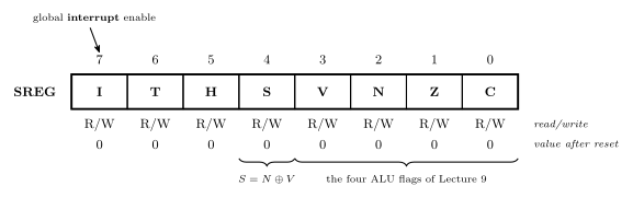
Figure 2: The status register, in the three-row form the datasheet uses: bit numbers above, flag names in the boxes, then the access row and the value each bit takes after reset. The callout names bit 7, the global interrupt enable; the braces underneath mark the four ALU flags and the sign flag \(S = N \oplus V\).
Instruction descriptions refer to these as SREG(n) by bit number:
| Flag | Bit | Meaning |
|---|---|---|
| C | SREG(0) | carry — was a carry out generated? |
| Z | SREG(1) | zero — was the result 0? |
| N | SREG(2) | negative — the sign bit of the result |
| V | SREG(3) | overflow — did a two’s complement addition/subtraction overflow? |
| S | SREG(4) | sign, \(= N \oplus V\) — the sign of the result corrected for any overflow |
| H | SREG(5) | half-carry — carry out of bit 3 |
| T | SREG(6) | transfer bit, used by BLD and BST |
| I | SREG(7) | global interrupt enable — set by sei, cleared by cli; cleared by the hardware when it takes an interrupt and set again by reti (avr-interrupts) |
C, Z, N and V are exactly the four flags of fetch-decode-execute-cycle.
S is not simply “the sign bit” — that is N. \(S = N \oplus V\) means: the result is negative (with no overflow), or would have been negative had overflow not occurred. That correction is what makes signed comparisons work, which is why the signed branches (BRLT, BRGE) test S while the unsigned ones (BRLO, BRSH) test C. The four cases — including the overflow case where N alone gives the wrong answer — are drawn in 2026-09-14-flow-of-control, and the branch pairs are tabulated in avr-branches-and-jumps.
The one-line meanings and the SREG(n) numbering are those of Atmel’s AVR Instruction Set Manual and the instruction summary in the ATmega324A datasheet. The I/O register map is the I/O register summary, pages 636–639 of the ATmega164A/324A/644A/1284P datasheet, which writes the I/O register number first and the data memory address in parentheses after it.
On-chip peripherals (ATmega324A)
Beyond the CPU and its memories, the chip carries a large set of peripherals — this is what makes it a microcontroller rather than a processor. The two figures nest: the whole of Figure 1 is what sits inside the single box marked AVR CPU in Figure 3.
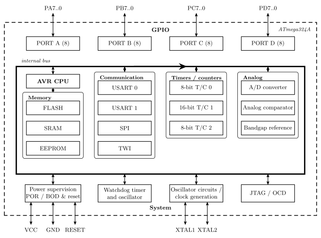
Figure 3: What is on the ATmega324A: the datasheet block diagram, rearranged into clusters by kind of thing — GPIO, memory, communication, timers/counters, analog and system. The dashed outline is the package boundary and the heavy rectangle inside it the internal bus, both as the datasheet draws them; the individual peripheral-to-port wiring is left out.
| Group | On the chip |
|---|---|
| General purpose I/O | PORT A, PORT B, PORT C, PORT D — four 8-bit ports |
| Communication | USART 0, USART 1, SPI, TWI |
| Timers/counters | 8-bit T/C 0, 16-bit T/C 1, 8-bit T/C 2 (T/C 3 is on the ATmega1284/1284P, not the 324A — the family datasheet’s block diagram covers both) |
| Analog | A/D converter, analog comparator, internal bandgap reference |
| Memory | Flash (program), SRAM (data), EEPROM (data, non-volatile) |
| System | Power supervision (POR/BOD & reset), watchdog timer and oscillator, oscillator/clock generation (XTAL1, XTAL2), JTAG/OCD |
There are three memories with three different jobs: flash for the program, SRAM for volatile working data, and EEPROM for data that must survive a power cycle. SRAM and EEPROM are the pair to keep straight: both hold data, and they differ only in surviving a power cycle.
See also
- cpu-organisation · fetch-decode-execute-cycle · instruction-set-architecture
- avr-instructions — the instruction set this hardware runs
- avr-io-ports — the I/O registers and the four GPIO ports
- avr-interrupts — the I bit, the vector table and the peripherals’ interrupt sources
- avr-timers-and-counters · avr-usart · avr-spi · analog-to-digital-conversion — four of the peripherals in detail
- memory-models · addressing-modes — the two address spaces, and how instructions name them
- assembly-process — flash, SRAM and EEPROM as the assembler’s three segments
- memory-technologies — flash, SRAM and EEPROM as technologies, and what the boot loader section is for · memory-hierarchy-and-cache — where the registers and SRAM sit by speed, and why the AVR needs no cache
- binary-number-representations — the flags’ two’s complement interpretation
- 2026-08-27-avr-introduction — Lecture 10
- 2026-08-31-instruction-set-architecture-part-1 — Lecture 11