SPI on the AVR
The Serial Peripheral Interface, and the ATmega324A’s SPI port: the four signals, how two shift registers exchange a byte, one transfer in time, the ways to connect several slaves, the pins, the three registers, the clock rate, code to send and receive, the interrupt, and the USARTs as extra SPI masters. Where SPI sits among serial links, next to the UART and I²C, is in serial-communication. First met in 2026-10-05-more-io. The datasheet covers the SPI on pages 166 to 174.
What SPI is
SPI is a synchronous serial bus with one master and one or more slaves (serial-communication).
- Synchronous: the master sends a clock, and both ends move a bit on each pulse of it. Nothing about speed has to be agreed beforehand, except that the master must not go faster than the slave can follow.
- Full duplex: there is a data wire in each direction, and every clock pulse moves one bit each way.
- The master starts every transfer and makes the clock. A slave only answers.
| Signal | Driven by | Carries |
|---|---|---|
| SCK (also written SCLK) | master | serial clock, one pulse per bit |
| MOSI | master | Master Out, Slave In |
| MISO | slave | Master In, Slave Out |
| \(\overline{\text{SS}}\) | master | Slave Select, active low: a slave takes part only while its \(\overline{\text{SS}}\) is 0 |
The names say which end drives each wire, so the wiring is MOSI to MOSI and MISO to MISO. It is not crossed over the way a UART’s Tx and Rx are.
The exchange: two shift registers in a ring
Master and slave each have an 8-bit shift register (shift-registers). MOSI joins the master’s MSB end to the slave’s LSB end, and MISO joins the slave’s MSB end to the master’s LSB end. Together they are one 16-bit register bent into a ring, and each SCK pulse rotates it by one place. The hardware view, with the clock generator and the select pins, is drawn in 2026-10-05-more-io.
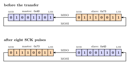
Figure 1: The exchange as data. Before the transfer the master’s register holds 0x4D, shaded blue, and the slave’s holds 0x73, shaded orange. Each SCK pulse moves every bit one place round the ring: towards the MSB inside each register, and across on MOSI or MISO at the ends. After eight pulses each byte has gone all the way across and the shading has changed sides: the master holds 0x73 and the slave 0x4D. A byte has been sent in each direction at once.
Two consequences follow from the ring:
- To receive, the master must send. There is no read-only transfer. To collect a byte from a slave, the master sends a dummy byte, often
0x00or0xFF, and keeps what comes back. - To send is also to receive. Every byte sent brings one back. If it is of no interest, the master reads it and throws it away.
Worked: one exchange, clock by clock
The master’s register holds 0x4D (0100 1101) and the slave’s holds 0x73 (0111 0011), and the bytes go most significant bit first. Each clock, each register’s top bit leaves on its data wire, the other seven move up one place, and the bit arriving from the other end fills the bottom:
| After clock | MOSI carried | MISO carried | Master | Slave |
|---|---|---|---|---|
| start | 0100 1101 |
0111 0011 |
||
| 1 | 0 | 0 | 1001 1010 |
1110 0110 |
| 2 | 1 | 1 | 0011 0101 |
1100 1101 |
| 3 | 0 | 1 | 0110 1011 |
1001 1010 |
| 4 | 0 | 1 | 1101 0111 |
0011 0100 |
| 5 | 1 | 0 | 1010 1110 |
0110 1001 |
| 6 | 1 | 0 | 0101 1100 |
1101 0011 |
| 7 | 0 | 1 | 1011 1001 |
1010 0110 |
| 8 | 1 | 1 | 0111 0011 |
0100 1101 |
The MOSI column, read down, is 0100 1101, the master’s byte, and the MISO column is 0111 0011, the slave’s. After 8 clocks the master holds 0x73 and the slave 0x4D.
One transfer in time
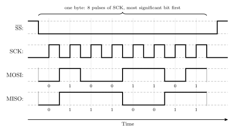
Figure 2: One SPI transfer in the AVR’s default mode: SCK idles low, both ends sample their incoming data wire on each rising edge of SCK (the dotted lines), and both put out their next bit on each falling edge. The master pulls \(\overline{\text{SS}}\) low to select the slave, and the slave’s first bit appears on MISO at that moment. Eight clock pulses then carry 0x4D from master to slave on MOSI and 0x73 from slave to master on MISO, most significant bit first, with the bit values written under each data wire. Raising \(\overline{\text{SS}}\) ends the transfer. The data wires matter only while \(\overline{\text{SS}}\) is low, so they are drawn only then.
A transfer, from the master’s side:
- Pull \(\overline{\text{SS}}\) low. The selected slave wakes up and puts its first bit on MISO.
- Write the byte to the data register. The SPI hardware makes eight pulses on SCK. On each rising edge both ends read the data wire coming in; on each falling edge both shift their next bit out.
- Wait for the transfer-complete flag, then read the byte that came in.
- Send more bytes the same way, or raise \(\overline{\text{SS}}\) to end the transfer.
The AVR’s SPI hardware never moves \(\overline{\text{SS}}\) itself in master mode. Steps 1 and 4 are the program’s job, done with PORTB.
Clock polarity and phase
The figure shows the AVR’s mode after reset. Two bits in the control register change it: CPOL, which level SCK rests at, and CPHA, whether data is read on the first or the second edge of each pulse. Together they number four modes:
| Mode | CPOL | CPHA | SCK when idle | Data read on |
|---|---|---|---|---|
| 0 | 0 | 0 | low | the rising edge, the first of each pulse |
| 1 | 0 | 1 | low | the falling edge, the second of each pulse |
| 2 | 1 | 0 | high | the falling edge, the first of each pulse |
| 3 | 1 | 1 | high | the rising edge, the second of each pulse |
A third setting is the bit order, MSB first or LSB first. A device’s datasheet says which mode and bit order it uses, and the master has to match it. As with a UART’s settings (serial-communication), nothing on the wires says which is in use, and a mismatch gives wrong bytes, not an error.
Several slaves
Both wirings are drawn in 2026-10-05-more-io.
Independent selects. SCK and MOSI go to every slave, and every slave’s MISO joins the one wire back to the master. Each slave has its own select line from the master, and the master pulls one low at a time. A slave whose \(\overline{\text{SS}}\) is high ignores SCK and lets go of MISO (the AVR as a slave makes all its SPI pins inputs), so only the selected slave drives the shared wire. Every slave costs one more master pin.
Daisy chain. One select line goes to all the slaves, and the data passes through them in turn: master MOSI into slave 1’s MOSI, each slave’s MISO into the next one’s MOSI, the last slave’s MISO back to the master’s MISO. The master’s register and the slaves’ registers make one ring, \(8 \times (\text{slaves} + 1)\) bits round. A chainable device acts on the byte it holds when \(\overline{\text{SS}}\) goes back high, so everything has to be in place by then.
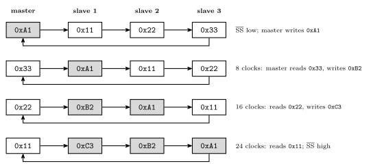
Figure 3: A daisy chain of three slaves as one long shift register, 32 bits round. Each row is the chain at one moment, read left to right in the direction the data moves, and the arrow underneath is the last slave’s MISO returning to the master. Shaded bytes are the ones the master has sent. Every 8 clocks move every byte one place along, so the first byte sent, 0xA1, ends up in the farthest slave, and the master receives the slaves’ old bytes, the farthest slave’s first. Between bytes the master reads what has arrived and writes the next byte to send.
Worked: which byte goes first?
To leave 0xA1 in slave 3, 0xB2 in slave 2 and 0xC3 in slave 1, send 0xA1, 0xB2, 0xC3, in that order, with \(\overline{\text{SS}}\) low for all 24 clocks. The byte for the farthest slave goes first, because every later byte pushes it one place further along. The three bytes that come back are the slaves’ previous contents, slave 3’s first.
The pins
The SPI port uses the upper half of port B (avr-io-ports):
| Port pin | Package pin | Signal | As master | As slave |
|---|---|---|---|---|
| PB4 | 5 | \(\overline{\text{SS}}\) | the program’s to use: make it an output | input |
| PB5 | 6 | MOSI | output: the program sets its DDRB bit |
input |
| PB6 | 7 | MISO | input | output: the program sets its DDRB bit |
| PB7 | 8 | SCK | output: the program sets its DDRB bit |
input |
Switching the SPI on forces some pins’ directions and leaves others to DDRB. A pin marked input is made an input by the hardware. A pin that has to be an output, the program has to make an output itself.
The \(\overline{\text{SS}}\) pin in master mode. If PB4 is left as an input and something pulls it low, the AVR takes it that another master is selecting it as a slave. It clears MSTR0, becoming a slave, and sets the transfer-complete flag. A master therefore makes PB4 an output, usually as the select line for its slave, or else guarantees that it stays high. As an output it is an ordinary port pin and the SPI ignores it.
These same pins are the ones a programmer uses to download a program into the AVR, which is worth remembering when a device is attached to them.
The registers
| Register | Holds |
|---|---|
SPCR0 |
control: on/off, master or slave, bit order, clock mode, clock rate, interrupt enable |
SPSR0 |
status: the transfer-complete and write-collision flags, and the double-speed bit |
SPDR0 |
data: write a byte to send it, read the byte received |
The datasheet’s SPI chapter (pages 172 and 173) calls these SPCR, SPSR and SPDR, and its bit names have no 0 either. In C and assembly every name carries the 0: SPCR0, SPE0, MSTR0, SPIF0, and SPR1 becomes SPR10. The I/O register summary still names the registers SPCR and SPSR, but writes the bit names with the 0, except that it labels bit 1 SPR01 where the header has SPR10.
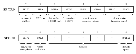
Figure 4: The SPI port’s two control and status registers, with the names used in code. SPCR0 sets the port up: bit 6 turns it on, bit 4 chooses master or slave, bit 5 the bit order, bits 3 and 2 the clock mode, and the bottom two bits the clock rate when it is a master. Bit 7 lets the end of a transfer raise an interrupt. In SPSR0, bit 7 is the flag that says a transfer has finished, bit 6 reports a write to the data register in the middle of a transfer, and bit 0 doubles the master’s clock rate, a third clock-rate bit to go with the two in SPCR0. Every bit is 0 after reset, so the port starts switched off.
SPCR0: the set-up
| Bit | Name | When 1 | When 0 |
|---|---|---|---|
| 7 | SPIE0 |
the end of a transfer raises an interrupt | no interrupt |
| 6 | SPE0 |
the SPI port is on | off: the pins belong to port B |
| 5 | DORD0 |
LSB first | MSB first |
| 4 | MSTR0 |
master | slave |
| 3 | CPOL0 |
SCK idles high | SCK idles low |
| 2 | CPHA0 |
data read on the second edge of each pulse | data read on the first edge |
| 1:0 | SPR10, SPR00 |
the clock rate, with SPI2X0 (below) |
SPSR0: what has happened
| Bit | Name | Set when | Cleared by |
|---|---|---|---|
| 7 | SPIF0 |
a transfer has finished; also when a master’s \(\overline{\text{SS}}\) input is pulled low | the interrupt handler running, or reading SPSR0 and then SPDR0 |
| 6 | WCOL0 |
SPDR0 was written while a transfer was going on |
reading SPSR0 and then SPDR0 |
| 0 | SPI2X0 |
(a setting) 1 doubles the master’s SCK |
Bits 5 to 1 are unused.
SPDR0: the data
Writing SPDR0 starts a transfer when the port is a master: the byte goes into the shift register and the eight clock pulses begin. Reading SPDR0 gives the byte received. The two directions are buffered differently. On the way out there is only the shift register, so a byte written during a transfer is not sent and sets WCOL0 instead. On the way in the finished byte is copied to a buffer, where it waits until the next byte is complete, so it has to be read before then or it is lost.
Choosing the clock rate
In master mode three bits pick the divider:
SPI2X0 |
SPR10 |
SPR00 |
SCK | At 8 MHz |
|---|---|---|---|---|
| 0 | 0 | 0 | \(f_{OSC}/4\) | 2 MHz |
| 0 | 0 | 1 | \(f_{OSC}/16\) | 500 kHz |
| 0 | 1 | 0 | \(f_{OSC}/64\) | 125 kHz |
| 0 | 1 | 1 | \(f_{OSC}/128\) | 62.5 kHz |
| 1 | 0 | 0 | \(f_{OSC}/2\) | 4 MHz |
| 1 | 0 | 1 | \(f_{OSC}/8\) | 1 MHz |
| 1 | 1 | 0 | \(f_{OSC}/32\) | 250 kHz |
| 1 | 1 | 1 | \(f_{OSC}/64\) | 125 kHz |
SPI2X0 halves the divider chosen by the other two. Eight codes give seven dividers, because 64 appears twice. After reset all three bits are 0, which is divider 4.
In slave mode these bits do nothing, because the slave’s clock comes from the master. A slave samples the incoming SCK with its own clock and is only guaranteed to keep up to \(f_{OSC}/4\), 2 MHz at 8 MHz.
A byte takes 8 SCK periods, which is \(8 \times\) divider CPU cycles: 16 cycles (2 µs) at the fastest, 1024 (128 µs) at the slowest.
Worked: the slowest master clock
Which bits must be 1 to switch the SPI on as a master with the slowest clock, and what is written to SPCR0?
The slowest divider is 128, code SPI2X0 SPR10 SPR00 = 0 1 1. Add SPE0 to switch the port on and MSTR0 to make it a master. Nothing in SPSR0 needs to be 1, since SPI2X0 must stay 0.
SPCR0 = (1<<SPE0) | (1<<MSTR0) | (1<<SPR10) | (1<<SPR00); /* 0101 0011 = 0x53 */Bits 6, 4, 1 and 0 make 0100 0000 + 0001 0000 + 0000 0010 + 0000 0001 = 0x53, and SCK is \(8\text{ MHz}/128 = 62.5\) kHz.
Worked: a 1 MHz clock
\(8\text{ MHz}/1\text{ MHz} = 8\), which is code 1 0 1: SPR00 in SPCR0 and SPI2X0 in SPSR0.
SPCR0 = (1<<SPE0) | (1<<MSTR0) | (1<<SPR00);
SPSR0 = (1<<SPI2X0);
Sending and receiving, by polling
A master that sends and receives one byte at a time:
#include <avr/io.h>

#define SS_PIN 4                          /* PB4 used as the slave's select */

void spi_init_master(void) {
    DDRB  |= (1<<SS_PIN) | (1<<5) | (1<<7);   /* SS, MOSI, SCK outputs; MISO stays an input */
    PORTB |= (1<<SS_PIN);                     /* SS high: no slave selected yet             */
    SPCR0  = (1<<SPE0) | (1<<MSTR0) | (1<<SPR00);   /* on, master, f/16 = 500 kHz        */
}

uint8_t spi_exchange(uint8_t out) {
    SPDR0 = out;                          /* writing starts the eight clocks   */
    while (!(SPSR0 & (1<<SPIF0))) {       /* wait for the transfer to finish   */
    }
    return SPDR0;                         /* the byte that came back; reading  */
                                          /* SPSR0 then SPDR0 clears SPIF0     */
}
and a transfer of two bytes, the second one to collect the slave’s reply:
uint8_t reply;

PORTB &= ~(1<<SS_PIN);                    /* select the slave                */
spi_exchange(0x4D);                       /* send; what comes back is ignored */
reply = spi_exchange(0x00);               /* send a dummy byte to read one   */
PORTB |= (1<<SS_PIN);                     /* deselect                        */
The rules it follows:
- The program moves \(\overline{\text{SS}}\), low before the first byte and high after the last.
- One byte at a time. Write
SPDR0, wait forSPIF0, then write the next. A write during a transfer is lost. - To read, send.
At 500 kHz the wait is 16 µs, 128 CPU cycles, against about a millisecond for a UART frame at 9600 baud. Waiting by polling (polling-and-interrupts) is often the sensible choice for SPI.
As a slave, the AVR only makes MISO an output and switches the port on with MSTR0 left at 0:
void spi_init_slave(void) {
    DDRB |= (1<<6);                       /* MISO is the slave's one output */
    SPCR0 = (1<<SPE0);                    /* on, slave                      */
}
A slave can never start anything. It puts the reply it wants to give in SPDR0 ahead of time, and when the master has clocked a byte through, SPIF0 is set and SPDR0 holds what the master sent.
The interrupt
| Event | Flag (SPSR0) |
Enable (SPCR0) |
Handler |
|---|---|---|---|
| transfer complete | SPIF0 |
SPIE0 |
ISR(SPI_STC_vect) |
It is vector 20 in the table (avr-interrupts), and running the handler clears SPIF0. The usual use is a queue of bytes: the handler reads the byte that has just arrived and writes the next one to SPDR0, so a run of bytes goes out without the main program waiting on each. On a slave, the interrupt is how the program finds out that the master has just exchanged a byte with it.
The USARTs as SPI masters
Each USART can also work as an SPI master, by setting its mode bits UMSELn1:0 in UCSRnC to 11 (avr-usart). Its pins then take the SPI roles:
| USART | SCK | Data out (MOSI) | Data in (MISO) |
|---|---|---|---|
| USART0 | XCK0, PB0 | TXD0, PD1 | RXD0, PD0 |
| USART1 | XCK1, PD4 | TXD1, PD3 | RXD1, PD2 |
There is no select pin: the program drives any spare port pin as \(\overline{\text{SS}}\). A USART in this mode can only be a master. With the SPI port as well, the ATmega324A can be the master on three separate SPI buses.
Common mistakes
- Crossing MOSI and MISO as if they were a UART’s Tx and Rx. MOSI goes to MOSI.
- Expecting to read without sending. The master gets a byte only by sending one.
- Leaving PB4 an input in master mode. If it floats or is pulled low,
MSTR0is cleared and the AVR silently becomes a slave. - Not setting
DDRBfor MOSI and SCK on a master, or MISO on a slave. Switching the SPI on does not make those pins outputs. - Waiting for the hardware to drive \(\overline{\text{SS}}\). A master has to do it in software.
- Writing
SPDR0before the last transfer has finished. The byte is not sent andWCOL0is set. - Using the datasheet names
SPCR,SPE,SPR1in code. The header names have a0:SPCR0,SPE0,SPR10. - Mismatched mode or bit order with the slave device: wrong bytes and no error.
- Clocking an AVR slave faster than \(f_{OSC}/4\).
- Loading a daisy chain nearest slave first. The first byte sent ends up in the farthest slave.
See also
- serial-communication — SPI next to the UART and I²C, bus masters and slaves, bit bashing
- shift-registers — the register at each end of the ring
- avr-io-ports — port B,
DDRB, and the pins’ alternate functions - avr-usart — the USART, and its mode bits for master SPI
- avr-interrupts · polling-and-interrupts — the
SPI_STCinterrupt, or waiting onSPIF0 - bit-masking · c-preprocessor-and-avr-headers —
(1<<SPE0)and where the names come from - week10-lab-adc-and-spi — Lab 16, the SPI port driving an LED matrix
- 2026-10-05-more-io — Lecture 19