Lecture 19 — More I/O
Two more ways for a microcontroller to talk to other chips, and the habits that make I/O code correct and readable. The first half is about buses: which device is in charge of a transfer, the two-wire I²C bus (TWI on the AVR), and SPI, a synchronous serial bus built from two shift registers joined in a ring, with the ATmega324A’s SPI port, its pins and its clock rates, and bit bashing for when the hardware is missing. The second half is AVR I/O coding: volatile for variables an interrupt handler changes, and setting, clearing and toggling bits of I/O registers by name. The reference notes are serial-communication, avr-spi, bit-masking and avr-io-ports.
Goals
- Say what makes a device a bus master or a bus slave, and why memory is always a slave.
- Describe the I²C bus and find the ATmega324A’s TWI pins.
- Explain how SPI sends a byte each way at once, using two shift registers joined in a ring.
- Connect several SPI slaves to one master, with a select line each or as a daisy chain.
- Find the SPI pins on the ATmega324A and work out an SPI clock rate from its divider.
- Say what bit bashing is and when it is the answer.
- Declare a variable
volatilewhen an interrupt handler changes it, and say what the optimiser does otherwise. - Set, clear and toggle single bits of an I/O register, with the bits named.
Bus masters and slaves
When several devices share wires, one of them has to decide when a transfer happens and which way it goes.
- The master is the device that initiates and controls the transfer of data. It decides when a transfer starts and which device it is with, and on a synchronous bus it also drives the clock.
- A slave waits for requests and responds to the master. It never starts a transfer of its own.
The roles belong to a transfer, not to a device for all time. Some devices can be masters and slaves, at different times. The ATmega324A’s SPI port and its TWI port can each be set up as either.
Memory can never be a bus master. It only ever answers a read or a write of an address that something else has chosen. On the AVR’s memory bus the CPU is the master and the memories are slaves.
Check. A CPU, a memory chip and an ATmega324A’s SPI port are on buses together. Which of them could start a transfer? The CPU, always. The SPI port, when it is set up as a master. The memory, never: it has no way to begin anything, only to answer.
I²C and TWI
I²C is the Inter-Integrated Circuit bus, created by Philips Semiconductor, now NXP. TWI, the Two-wire Interface, is the name Atmel uses for it. Both are synchronous serial: one of the wires is a clock (serial-communication).
Every device on the bus, device 1 to device n, connects to the same two wires:
| Wire | Carries |
|---|---|
| SDA | serial data, in either direction |
| SCL | serial clock, driven by the master |
Two wires serve many devices, and adding one adds no wires. The price is that every device sees every transfer, so the master begins each one by sending the address of the slave it wants, and the others ignore it. With one data wire, data goes one way at a time. The bus is drawn, with the pull-up resistors that make the sharing work, in serial-communication.
TWI on the ATmega324A
- The ATmega324A has one TWI port.
- Its two wires are an alternate use of two port C pins: PC0 is SCL and PC1 is SDA. While the TWI is switched on, those pins belong to it, not to
PORTC. - The datasheet describes the TWI in full on pages 211 to 239.
SPI
SPI is the Serial Peripheral Interface. The master and the slave each hold an 8-bit shift register (shift-registers), and the wires join the two registers into one ring. There are four signals:
| Signal | Driven by | Carries |
|---|---|---|
| SCK (also written SCLK) | master | the serial clock, one pulse per bit |
| MOSI | master | Master Out, Slave In: data to the slave |
| MISO | slave | Master In, Slave Out: data to the master |
| \(\overline{\text{SS}}\) | master | Slave Select, active low: 0 selects the slave |
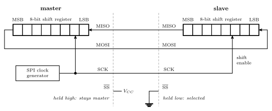
Figure 1: SPI as two 8-bit shift registers joined in a ring. Each pulse of SCK, made by the master’s clock generator, shifts both registers one place towards the MSB. At the slave, SCK is the register’s shift enable, so the slave’s register moves only when a pulse arrives from the master. The master’s MSB leaves on MOSI and enters the slave at its LSB, while the slave’s MSB leaves on MISO and enters the master at its LSB. After eight pulses the two bytes have changed places, so every transfer moves a byte in each direction. The dashed lines are the edges of the two chips, with the pin names just inside them and the wiring between. The slave’s \(\overline{\text{SS}}\) is tied to ground, so it is always selected; the master’s own \(\overline{\text{SS}}\) is tied to \(V_{CC}\), which keeps it a master.
How the ring moves a byte. On each clock pulse both registers shift one place towards the MSB, at the same moment. At the slave, SCK is the register’s shift enable: the slave’s register moves only when a pulse arrives from the master. The bit that falls off the master’s MSB end goes out on MOSI and into the slave’s LSB end; the bit that falls off the slave’s MSB end goes out on MISO and into the master’s LSB end. Neither register gains or loses anything overall: the two of them are a single 16-bit register rotating. After eight pulses every bit has moved eight places, which carries the master’s byte entirely into the slave and the slave’s byte entirely into the master.
So every SPI transfer is an exchange. To read a byte from a slave the master has to send one, even a meaningless one, and every byte sent brings one back, which the master may simply ignore.
The master’s clock generator decides when every bit moves, so the slave never has to time a bit for itself, and nothing has to be agreed about speed beyond the fastest the slave can follow. That is the advantage of a synchronous link over a UART, where both ends must be set to the same baud rate beforehand.
Worked: one exchange
The master’s register holds 0x4D and the slave’s holds 0x73, most significant bit first. What travels on each data wire, and what does each register hold after eight clocks?
MOSI carries the master’s byte, MSB first: 0 1 0 0 1 1 0 1. MISO carries the slave’s: 0 1 1 1 0 0 1 1. After eight clocks the master holds 0x73 and the slave holds 0x4D. The register contents after each clock are tabulated in avr-spi.
Several slaves
One master can drive several slaves, wired in either of two ways.
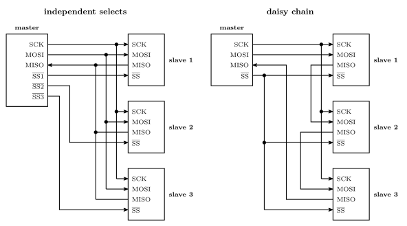
Figure 2: Two ways to give one SPI master three slaves. Left, independent selects: SCK and MOSI go to every slave, every slave’s MISO joins the one wire back to the master, and each slave has a select line of its own. The master pulls one select low at a time, and a slave that is not selected lets go of MISO, which is what lets them share it. Right, a daisy chain: one select line goes to all three, and the data goes through them in turn, from the master’s MOSI into slave 1, out of each slave’s MISO into the next one’s MOSI, and from the last slave’s MISO back to the master. A dot is a connection; lines that cross without a dot are not connected.
Independent selects. SCK and MOSI go to every slave, and all the slaves’ MISO pins share the one wire back. Each slave gets its own select line, \(\overline{\text{SS1}}\), \(\overline{\text{SS2}}\), \(\overline{\text{SS3}}\), and the master pulls exactly one of them low for a transfer. An unselected slave ignores the clock and lets go of MISO, so only the selected one drives it. Each extra slave costs the master one more pin.
Daisy chain. One select line for all of them, and the data passes through each slave on its way round: master MOSI to slave 1, each slave’s MISO to the next slave’s MOSI, the last slave’s MISO back to the master’s MISO. The registers now make one long ring, 8 bits for the master and 8 more for each slave. It needs no extra pins however many slaves there are, but every transfer goes through all of them.
Worked: loading a daisy chain
Three slaves are daisy-chained and the master wants 0xA1 in slave 3, 0xB2 in slave 2 and 0xC3 in slave 1. In what order does it send the bytes, for how many clocks, and what comes back?
Each byte sent pushes every byte already in the chain one slave further along, so the byte meant for the farthest slave has to go first: 0xA1, then 0xB2, then 0xC3, with \(\overline{\text{SS}}\) held low for all 24 clocks. After the first 8, 0xA1 is in slave 1; the next 8 push it to slave 2 and put 0xB2 in slave 1; the last 8 push it to slave 3. What comes back to the master is what the slaves held before, the farthest slave’s old byte first: if they held 0x11, 0x22 and 0x33, the master receives 0x33, 0x22, 0x11. The step-by-step picture is in avr-spi.
SPI on the ATmega324A
- The ATmega324A has one SPI port.
- It shares pins with the upper half of port B: PB4 is \(\overline{\text{SS}}\), PB5 is MOSI, PB6 is MISO and PB7 is SCK.
- The hardware generates the signals. The program writes one byte; the port makes the eight clock pulses and does the shifting by itself.
- It can be a master or a slave, chosen by a bit in its control register.
- The datasheet covers it on pages 166 to 174.
- The USARTs can also be used as SPI masters, which gives the chip up to three (avr-spi).
Inside the chip the SPI block is wired to port B, the TWI block to port C, and the two USARTs to port D, apart from USART0’s clock pin on port B (the chip’s other blocks are in avr-architecture). The pins are:
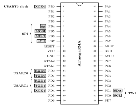
Figure 3: The ATmega324A’s 40 pins, with the serial interfaces marked. Each pin is named for its port bit, and the boxed names are the alternate uses that matter here. The SPI port is the upper half of port B, PB4 to PB7. The TWI is PC0 and PC1. USART0 receives and transmits on PD0 and PD1, and USART1 on PD2 and PD3; XCK0 and XCK1 are the USARTs’ clock pins, which is where the clock comes out when a USART works as an SPI master. Whichever interface is switched on takes its pins over from the port.
The datasheet’s pinout is shared with bigger chips in the same family, and some pins also list functions of a fourth timer (T3, ICP3, OC3A, OC3B) that the ATmega324A does not have, just as its block diagram shows a 16-bit T/C 3 (2026-08-27-avr-introduction).
The SPI clock rate
As a master, the AVR makes SCK by dividing its own clock, and the divider can be chosen. With the 8 MHz clock:
| Divider | SCK |
|---|---|
| 2 | 4 MHz |
| 4 | 2 MHz |
| 8 | 1 MHz |
| 16 | 500 kHz |
| 32 | 250 kHz |
| 64 | 125 kHz |
| 128 | 62.5 kHz |
As a slave, the fastest SCK it can follow is \(f_{OSC}/4\), 2 MHz at 8 MHz. A slave does not run its SPI logic from SCK directly. It samples the incoming SCK with its own clock, and each high and each low half of SCK has to last a couple of its own clock cycles to be seen reliably. Which bits choose the divider is in avr-spi.
Worked: how long does a byte take?
A byte is 8 SCK periods, and each period is divider CPU clock cycles.
| Divider | CPU cycles per byte | Time per byte at 8 MHz |
|---|---|---|
| 2 | \(8 \times 2 = 16\) | 2 µs |
| 16 | \(8 \times 16 = 128\) | 16 µs |
| 128 | \(8 \times 128 = 1024\) | 128 µs |
For comparison, one 8N1 UART frame at 9600 baud takes \(10 / 9600 \approx 1.04\) ms, about 500 times as long as an SPI byte at the fastest rate.
Worked: two AVRs
Two ATmega324As, both on 8 MHz clocks, are joined by SPI. What is the fastest master setting that works? The slave can follow at most \(8\text{ MHz}/4 = 2\) MHz, so the master’s divider must be 4 or more. Divider 2 gives 4 MHz, which a master can produce but this slave cannot follow.
Bit bashing
Sometimes a microcontroller has no hardware support for a bus standard, or not enough interfaces of that standard: a second SPI bus wanted on a chip with one SPI port, say. The standard can then be simulated with general purpose port pins. The program drives each output pin and reads each input pin itself, one edge at a time, in the order the standard lays down. This is bit bashing, also called bit banging.
For an SPI master, each of the eight bits is four steps on ordinary pins: put the next bit on the MOSI pin, raise the SCK pin, read the MISO pin, lower the SCK pin. The code, and what it costs, are in serial-communication.
Bit bashing suits a synchronous standard well. The master makes the clock, so if the program is held up between two edges, by an interrupt for instance, the transfer just pauses and nothing goes wrong. An asynchronous standard such as a UART has no clock to wait for, so a bit-bashed UART has to time every bit exactly.
Worked: one SPI port, two SPI buses
A design on the ATmega324A needs to be the master on two separate SPI buses, and the SPI port is already in use for one of them. What are the options for the other?
- A USART in master SPI mode. Hardware does the shifting, as with the SPI port, on the USART’s XCK, TXD and RXD pins (avr-spi).
- Bit bashing on any three spare port pins, plus one for the select. It works anywhere, but the CPU does all of the work and the bus runs much slower.
If the second “bus” is really just more slaves, neither is needed: one SPI port drives several slaves through separate select lines.
AVR I/O coding
Volatile variables
volatile int running;volatile tells the compiler that the variable can change outside the standard flow of control: in an interrupt handler, or in another thread. The compiler must then not apply the optimisations that assume only the code in front of it changes the variable. Every read in the source becomes a real read of memory, and every write a real write.
Worked: a loop that never ends
A button on INT0 is meant to start the program running:
volatile int running;

ISR(INT0_vect) {
    running = 1;              /* the button has been pushed */
}

int main(void) {
    /* ... set up INT0 for the button, then sei() ... */
    running = 0;
    while (!running) {
        ;                     /* do nothing until the button is pushed */
    }
    /* carry on */
}
What does an optimising compiler do with the loop if running is declared without volatile?
It changes the loop to
while (1) {
    ;
}
The compiler looks at main on its own. It has just set running to 0, and nothing inside the loop writes running, so as far as it can tell !running is true every time and testing it again is wasted work. The handler is a separate function that main never calls, so its write is invisible to that reasoning. The result is a program that never leaves the loop, however often the button is pushed. With volatile, each test of !running reads the variable from memory, and the first test after the handler has run sees 1 and the loop ends.
The register names PINC, PORTA and the rest are volatile for the same reason: a pin can change without the program changing it (c-preprocessor-and-avr-headers). On this 8-bit CPU a one-byte uint8_t is a better type for a flag than int, because it is read in a single instruction and an interrupt cannot land halfway through (avr-interrupts). The two-column picture of what volatile changes is in 2026-09-21-interrupts.
Setting I/O register bits
When setting or clearing particular bits of an I/O register, be explicit about which bits. These three lines all have the same effect:
| Code | What the reader has to do | |
|---|---|---|
| Poor | TCCR1B = 10; |
convert 10 to binary, then look up what each 1 is |
| Better | TCCR1B = 0x0A; |
read the bits off the hex, then look them up |
| Best | TCCR1B = (1<<WGM12)\|(1<<CS11); |
nothing: the two bits being set are named |
Worked: are they really the same?
\(10 = 8 + 2\), which is 0000 1010, which is 0x0A. In TCCR1B, WGM12 is bit 3 and CS11 is bit 1, so
\[(1 \ll 3)\ |\ (1 \ll 1) = \texttt{0000 1000}\ |\ \texttt{0000 0010} = \texttt{0000 1010}\]
All three are the same byte, and since the compiler works out (1<<WGM12)|(1<<CS11) while compiling, all three produce the same machine code. The readable form costs nothing.
And what does it do? WGM12 = 1, with WGM13 cleared by the same write and WGM11:10 left at 0 in TCCR1A, makes WGM13:0 = 0100: CTC mode with the top of the count in OCR1A. CS12:0 = 010 divides the clock by 8. It is the set-up for the 10 ms tick in week9-lab-avr-interrupts (avr-timers-and-counters). The best form says so to anyone who knows the bit names. The poor form says nothing.
Where the names come from
The register and bit names are the datasheet’s. Each register is drawn in its section of the datasheet with its address and its bits. The datasheet has errors in places, so check a name against the I/O register summary at the back before trusting it. The SPI port is a case in point: its own chapter calls the enable bit SPE and the master bit MSTR, but the names that compile are SPE0 and MSTR0, which is how the summary writes them (avr-spi). For timer/counter 0’s TCCR0B, on page 112:
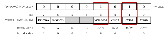
Figure 4: Timer/counter 0’s control register B in the datasheet’s three-row form: bit numbers above, names in the boxes, then whether each bit can be read or written and its value after reset. The register is I/O register 0x25, data address 0x45. Bits 5 and 4, shaded grey, are unused and read as 0; the two FOC bits can only be written. Each bit name is defined in the device header as its bit number, so WGM02 is 3 and CS01 is 1, and shifting 1 left by that number puts a 1 in the named column. The two outlined columns follow each name up through its bit number to its 1 in the top row: ORed together, (1<<WGM02)|(1<<CS01) is 0000 1010, which is 0x0A.
Bit names are macros, defined in the device header that <avr/io.h> pulls in:
#define WGM02 3A bit name is the bit’s number, not its mask. That is why it is always written (1<<WGM02): the shift turns the number 3 into the mask 0000 1000.
The same names work in assembly, where the assembler works out the expression:
ldi r16, (1<<WGM02)|(1<<CS01)Worked: what does that load?
WGM02 is 3 and CS01 is 1, so the constant is 0000 1000 | 0000 0010 = 0x0A, and the instruction in flash is simply ldi r16, 0x0A. To put it in the register takes out TCCR0B, r16, which works because TCCR0B is I/O register 0x25, inside the 64 that out can reach (avr-io-ports).
It is the same byte as TCCR1B = 0x0A above, and it shows why the names matter. In TCCR1B, bit 3 is WGM12, one bit of timer 1’s four-bit mode, and 0x0A gives CTC. In TCCR0B, bit 3 is WGM02, the top bit of timer 0’s three-bit mode, and with TCCR0A’s two mode bits at 0 it makes the mode 100, which is reserved: no use at all. Timer 0’s CTC mode is WGM01, in TCCR0A. A bit name means something only in its own register, and (1<<WGM12) written into TCCR0B would quietly set WGM02, because both are bit 3.
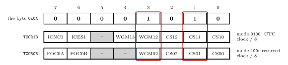
Figure 5: One byte, two registers, two meanings. The byte 0x0A has its 1s in bits 3 and 1, outlined. In TCCR1B those bits are WGM12 and CS11; in TCCR0B the same positions are WGM02 and CS01, because bit names are only bit numbers. The clock select field lines up in both, so the clock is divided by 8 either way. The mode does not: with the mode bits in TCCR1A and TCCR0A left at 0, bit 3 makes timer 1’s four-bit mode 0100, CTC, and timer 0’s three-bit mode 100, a reserved code that should not be used. Unused bits are shaded grey.
Clearing and toggling I/O register bits
The same rules apply: name the bit, and change only that bit.
PORTC &= ~(1<<5);         /* clear bit 5 of port C's output: PC5 driven low   */
TIMSK2 ^= (1<<OCIE2A); /* toggle the timer 2 output compare A interrupt enable */- To clear a bit, AND with a mask that has a 0 on that bit and 1s everywhere else.
~(1<<5)is the complement of0010 0000, which is1101 1111. ANDing with 1 keeps a bit and ANDing with 0 clears it. - To toggle a bit, XOR with a mask that has a 1 on that bit.
OCIE2Ais bit 1 ofTIMSK2, so the mask is0000 0010. XOR with 1 flips a bit and XOR with 0 keeps it. - To set a bit, OR with a 1 on it, as above.
Each of these reads the register, changes one bit and writes it back, leaving the other seven alone. Set, clear and toggle side by side on one byte are drawn in bit-masking.
Worked: clear bit 5 of port C
Which register does the clear go to?
PORTC, the register that holds the values port C drives: PORTC &= ~(1<<5); makes PC5 go low and leaves the other seven outputs as they were. Not PINC. PINC holds the levels on the pins, it is not a store, and on this chip writing a 1 to a bit of PINC toggles the matching bit of PORTC. PINC &= ~(1<<5) reads the pins, clears bit 5 of that reading and writes it back, which flips every other output that happened to read high and leaves PC5 alone: the opposite of what was wanted. The details are in avr-io-ports.
Worked: does this line enable the interrupt?
/* enable output compare A interrupt for timer 2 */
TIMSK2 ^= (1<<OCIE2A);
Only if it was off. XOR flips the bit. If OCIE2A was 0 this sets it and the interrupt is enabled; if it was already 1, the same line clears it and disables the interrupt. Run twice, it undoes itself. To enable, whatever the bit was before, set it:
TIMSK2 |= (1<<OCIE2A);    /* enable  */
TIMSK2 &= ~(1<<OCIE2A);   /* disable */
Toggling is for things that are meant to alternate, like blinking an LED with PORTC ^= (1<<0); from a timer handler.
See also
- serial-communication — masters and slaves, I²C with its pull-ups, SPI next to the UART, bit bashing in code
- avr-spi — the SPI port in full: the exchange clock by clock, timing, several slaves, the registers, the clock rate bits, code
- bit-masking — set, clear and toggle as bitwise operations, and writing registers by bit name
- avr-io-ports — changing one bit of a port, writing to
PINx, the pins’ alternate functions - avr-interrupts · 2026-09-21-interrupts —
volatileand interrupt handlers - c-preprocessor-and-avr-headers — where the register and bit names are defined
- avr-timers-and-counters — the fields of
TCCR0BandTCCR1B - shift-registers — the heart of SPI
- week10-lab-adc-and-spi — Lab 16, the SPI port driving an LED matrix
- 2026-09-24-serial-io — Lecture 18 · 2026-10-08-assembly-process — Lecture 20