Lab 16 — A/D and SPI
Learning Lab 16: two more of the ATmega324A’s peripherals, each with a device to drive. The analog to digital converter reads a joystick, and the SPI port sends commands to an LED matrix. Five tasks build from wiring the joystick up to an Etch-A-Sketch that draws on the matrix with it. The converter is in analog-to-digital-conversion, the SPI bus in avr-spi, the joystick and the LED matrix in io-board, and the timer used to pace the programs in avr-timers-and-counters. The lectures behind it are 2026-09-24-serial-io (Lecture 18) and 2026-10-05-more-io (Lecture 19).
Outline
- The A/D converter, used to read the joystick
- SPI, used to drive the LED matrix
- One timer question, about a slow count for pacing a program
- Five tasks, worked in full at the end
The A/D converter
The facts the lab relies on (analog-to-digital-conversion):
- The port A pins can be used as analog inputs.
- There is one converter, behind an analog multiplexer, so one input is converted at a time.
- The reference voltage can be chosen. The lab uses the supply, \(V_{cc} = 5\ \text{V}\), which reaches the converter as AVCC.
- The resolution is 10 bits: results from 0 to 1023.
- A conversion takes time: up to 3200 clock cycles, 0.4 ms at 8 MHz. The converter runs on its own clock, and a conversion takes 13 of its cycles, 25 for the first one after it is switched on. At the slowest setting, the clock divided by 128, that first conversion is \(25 \times 128 = 3200\) cycles. A faster converter clock gives a quicker answer with fewer accurate bits.
- So the program has to find out when a conversion has finished, either by polling the start bit
ADSC, which reads 1 until the result is ready, or by taking the interrupt at the end of the conversion (polling-and-interrupts).
Worked: the ADC clock prescaler
The ADC clock needs to run between 50 kHz and 200 kHz for full precision. What are the bounds for the ADC clock prescaler?
A. 80 to 320 · B. 40 to 160 · C. 20 to 80 · D. 25 to 100 · E. 50 to 150 · F. 160 to 640 · G. 30 to 120 · H. 10 to 40
B. The ADC clock is the 8 MHz system clock divided by the prescaler \(N\), so
\[50\ \text{kHz} \le \frac{8\ \text{MHz}}{N} \le 200\ \text{kHz} \quad\Longleftrightarrow\quad \frac{8\ \text{MHz}}{200\ \text{kHz}} \le N \le \frac{8\ \text{MHz}}{50\ \text{kHz}} \quad\Longleftrightarrow\quad 40 \le N \le 160.\]
A bigger divisor gives a slower clock, so the upper frequency limit sets the lower bound on \(N\). The bounds are in the ratio 4 to 1 because the frequencies are, and most of the other options have that ratio too: A, C, D, F, G and H are the right answers for system clocks of 16, 4, 5, 32, 6 and 2 MHz. E, 50 to 150, is not in the ratio 4 to 1 and is right for no clock.
The prescaler only offers powers of two, 2 to 128, so two settings land in the window: 64, giving 125 kHz, and 128, giving 62.5 kHz. The programs below use 64, which puts the clock in the middle of the window and makes a conversion \(13 \times 64 = 832\) cycles, 104 µs.
Worked: the ADMUX value
What value needs to go in ADMUX to use AVCC as the reference voltage, right adjust the result and select input ADC1?
ADMUX holds three fields (analog-to-digital-conversion):
| Field | Bits | Wanted | Value |
|---|---|---|---|
REFS1:0, reference |
7, 6 | AVCC | 01 |
ADLAR, adjust |
5 | right adjusted | 0 |
MUX4:0, input |
4 to 0 | ADC1 on its own | 00001 |
Put together, 0100 0001, which is 0x41. In C, ADMUX = (1<<REFS0) | 1;, or (1<<REFS0) | (1<<MUX0).

Figure 1: The value 0x41 in ADMUX, bit by bit. The top two bits choose the reference voltage, and 01 means AVCC, the 5 V supply. Bit 5 chooses how the 10-bit result sits in its 16-bit register, and 0 means right adjusted, so it reads as a number from 0 to 1023. The bottom five bits choose the input, and 00001 is ADC1, pin PA1. The two shaded bits are the ones set.
The joystick
The joystick is a small board made to sit in the breadboard. Each axis is a potentiometer between its own supply pin and ground, and the stick moves the wiper, so each axis gives a voltage between 0 and 5 V (io-board):
| Pin | Connect to | What it is |
|---|---|---|
| L/R+ and U/D+ | VCC, 5 V, both of them | the top end of each potentiometer |
| GND (two of them) | GND, one is enough | the bottom end of both |
| L/R (two of them) | an analog input | x: 0 V with the stick to the left, 5 V to the right |
| U/D (two of them) | an analog input | y: 0 V at the bottom, 5 V at the top |
The pins come in pairs that are joined on the board, so only one L/R, one U/D and one GND need a wire. The two + pins are not joined to each other, so both need one.
Where it goes. At the right-hand end of the breadboard, leaving room for the microcontroller board and its programmer to the left. Turned the right way, the X arrow printed on the board points to the top of the breadboard. So the stick’s own left and right, the direction x measures, run along the breadboard from bottom to top, and its up and down run from right to left. The board’s pins are protected by a piece of black foam when it is not in use, which is worth keeping.
The programs below use PA0 (ADC0) for x and PA1 (ADC1) for y.
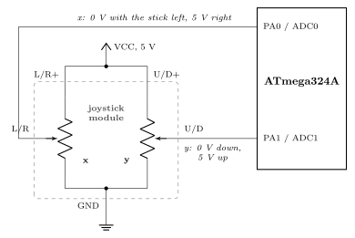
Figure 2: The joystick wired to the microcontroller. Each axis is a potentiometer from its own supply pin down to ground, and the stick sets the wiper, so the wiper voltage goes from 0 V to 5 V as the stick crosses from one side to the other. The two supply pins, L/R+ and U/D+, are separate and both go to VCC. The x output goes to PA0, which is analog input ADC0, and the y output to PA1, ADC1. The module’s second L/R, U/D and GND pins are joined to these inside it and are left unconnected.
Worked: the stick pulled down
The joystick is seen from above, turned a quarter turn clockwise from the way it sits in the breadboard, so that its L/R+ and U/D+ pins are at the top corners and its two GND pins at the bottom corners. That puts its own x axis across and its y axis up. The stick is pulled straight towards the bottom edge. What (x, y) should the ADC read?
A. (−511, 0) · B. (−511, 511) · C. (−511, 1023) · D. (0, −511) · E. (0, 511) · F. (0, 1023) · G. (511, −511) · H. (511, 0) · I. (1023, −511) · J. (1023, 0)
H, (511, 0). Straight down leaves x where it rests, in the middle, and takes y as low as it goes.
- x is in the middle of its range. The wiper sits halfway, 2.5 V, and halfway through 0 to 1023 is 511.5. A reading of 511 or 512 both mean centred.
- y is at the bottom of its range, 0 V, which reads 0.
- No reading is negative. The converter’s result is an unsigned number from 0 to 1023, so every option with \(-511\) in it is out. Those are what a reading measured from the centre would look like, which a program can work out by subtracting 511, but the converter itself never reports.
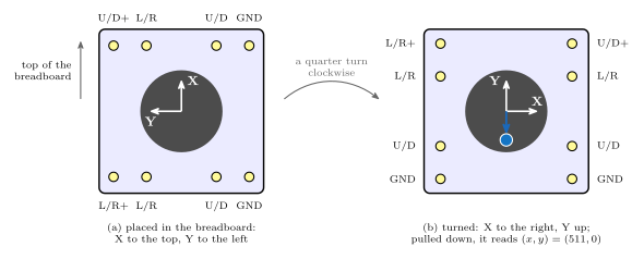
Figure 3: Why the stick’s x runs across and its y runs up in this view. The X and Y arrows printed under the stick mark the directions in which L/R and U/D rise from 0 V to 5 V. Placed in the breadboard (a), X points to the top of the breadboard and Y to the left. A quarter turn clockwise (b) puts L/R+ and U/D+ at the top corners and the GND pins at the bottom corners, and turns X to point right and Y up, so the readings are laid out the usual way. The blue dot is the stick, pulled towards the bottom edge. That is at right angles to X, so x stays at the centre of its range, and straight against Y, so y is at its lowest.
It is “should”, not “will”. A real stick at rest sits a few counts away from 511, and when pulled all the way it may not quite reach 0 V. A program that tests for “centred” or “pushed down” needs a margin either side, as the programs below have.
Worked: where is (614, 689)?
The ADC is reading (x, y) = (614, 689). Where is the joystick? There are two parts to the answer, which way the stick is pushed and how far.
A. 15° anticlockwise of the right half-axis · B. 30° · C. 45° · D. 60° · E. 75°
F. 20 % tilted · G. 40 % tilted · H. 60 % tilted · I. 80 % tilted · J. 100 % tilted
D and G: 60° anticlockwise of the right half-axis, 40 % tilted. Measure from the centre, (511, 511):
\[\Delta x = 614 - 511 = 103, \qquad \Delta y = 689 - 511 = 178.\]
Both are positive, so the stick is up and to the right. Its direction, as an angle measured anticlockwise from straight right, is
\[\theta = \tan^{-1}\frac{\Delta y}{\Delta x} = \tan^{-1}\frac{178}{103} = \tan^{-1} 1.728 = 59.9^\circ \approx 60^\circ.\]
How far it is pushed is its distance from the centre, as a fraction of the 511 counts from the centre to full deflection:
\[\frac{\sqrt{103^2 + 178^2}}{511} = \frac{205.7}{511} = 0.40, \quad\text{so } 40\,\%.\]
Working backwards confirms it. Taking the exact centre, 511.5, full deflection is 511.5 counts, and 40 % of it is 204.6. At 60° that is \(204.6 \cos 60^\circ = 102.3\) across and \(204.6 \sin 60^\circ = 177.2\) up, which lands on (613.8, 688.7), and the converter reports whole numbers, (614, 689). Mixing up the axes gives 30°, since (689, 614) is the reading at 30°.
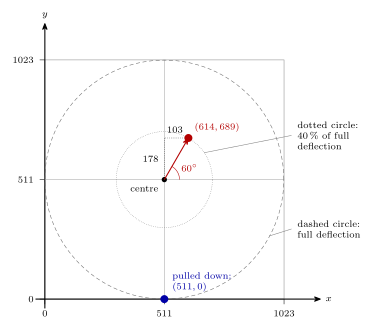
Figure 4: The joystick’s readings as a plane, x across and y up, each from 0 to 1023, with the centre at (511, 511). The dashed circle is full deflection, 511 counts from the centre. Pulling the stick straight down gives (511, 0): x stays centred and y goes to the bottom of its range. The reading (614, 689) is 103 counts right of the centre and 178 up. That is 206 counts from the centre, 40 % of full deflection, at 60° anticlockwise from the right half-axis. No reading is ever negative: the converter’s result runs from 0 to 1023.
SPI
SPI, the Serial Peripheral Interface, is the AVR’s synchronous serial port (avr-spi). The master and the slave each have an 8-bit shift register, and the two are joined in a ring: MOSI carries bits out of the master’s most significant end into the slave’s least significant end, and MISO carries bits out of the slave’s most significant end back into the master’s least significant end. The master makes the clock, SCK, and each pulse shifts both registers one place, so after eight pulses the two bytes have changed places. The slave takes part only while its select line, \(\overline{\text{SS}}\), is held low. With one master and one slave, the simplest arrangement holds the master’s own \(\overline{\text{SS}}\) high, so that it stays the master, and ties the slave’s low, so that it is always selected.
Sending a byte is writing it to the data register, and like a conversion it takes time: eight clock pulses. The program finds out it has finished by polling the flag SPIF0, or by taking the “serial transfer complete” interrupt, SPI_STC.
The names in code
The datasheet describes the SPI registers on pages 172 and 173 as SPCR and SPSR, but the ATmega324A header names them SPCR0 and SPSR0, with a 0 for SPI port 0. Their bit names take a 0 on the end as well: SPIE is SPIE0, SPE is SPE0, and SPR1 is SPR10. The data register follows the same pattern, SPDR0.
The datasheet’s register summary already has the 0s, with one slip: the bit printed there as SPR01 is SPR10.
Worked: master mode, slowest clock
Which bits of the SPI control registers SPCR and SPSR need to be set (1) to enable SPI in master mode with the slowest possible clock rate?
In SPCR0: SPE0, MSTR0, SPR10 and SPR00. In SPSR0: none. So SPCR0 = 0x53.
SPE0, bit 6 ofSPCR0, switches SPI on.MSTR0, bit 4, makes the AVR the master, the end that drives the clock.- The clock rate is set by three bits in two registers,
SPI2X0inSPSR0andSPR10:SPR00inSPCR0:
SPI2X0 |
SPR10 |
SPR00 |
SCK |
|---|---|---|---|
| 0 | 0 | 0 | clock / 4 |
| 0 | 0 | 1 | clock / 16 |
| 0 | 1 | 0 | clock / 64 |
| 0 | 1 | 1 | clock / 128 |
| 1 | 0 | 0 | clock / 2 |
| 1 | 0 | 1 | clock / 8 |
| 1 | 1 | 0 | clock / 32 |
| 1 | 1 | 1 | clock / 64 |
SPI2X0 doubles the speed, so the slowest rate has it at 0 and both SPR bits at 1: \(8\ \text{MHz} / 128 = 62.5\ \text{kHz}\). One byte then takes \(8 / 62\,500 = 128\ \text{µs}\).
The other bits stay 0: no interrupt (SPIE0), the most significant bit first (DORD0), and the clock idling low with data sampled on its rising edge (CPOL0, CPHA0). SPIF0 and WCOL0, the top two bits of SPSR0, are flags the hardware sets, not settings.
SPCR0 = (1<<SPE0) | (1<<MSTR0) | (1<<SPR10) | (1<<SPR00); /* 0x53 */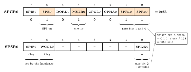
Figure 5: The two SPI registers set for master mode at the slowest clock. In SPCR0 the shaded bits are set: SPE0 turns SPI on, MSTR0 makes the AVR the master, and SPR10 and SPR00 select the slowest rate. The rate is the one setting split across two registers. Its third bit, SPI2X0, is bit 0 of SPSR0, and it stays 0, since setting it would double the speed. The top two bits of SPSR0 are status flags that the hardware sets.
The LED matrix
The LED matrix is 16 columns by 8 rows of pixels, each with a red and a green LED. It is an SPI slave: it takes commands, one byte at a time, from the AVR. It has two connection headers (io-board):
- K1, two pins, is its power. A two-wire lead joins it to the I/O board’s connector J1, VCC on the left pin and GND on the right.
- K2, four pins, is the SPI connection. It goes to the AVR’s SPI port, PB7 to PB4: SCK on PB7, MISO on PB6, MOSI on PB5 and \(\overline{\text{SS}}\) on PB4. The order of the four pins on K2 has to be matched against the pin names in the datasheet before the lead is plugged in.
The matrix’s reference manual describes everything it understands. The programs here use two commands, which are enough to draw anything.
The SPI pins are also the programming pins. The programmer loads the AVR’s flash through PB7 to PB5, so the matrix sees the programming traffic too, takes it for nonsense commands, and can end up showing Err. To clear it, hold the AVR’s reset button down for at least half a second after programming, then let the program start.
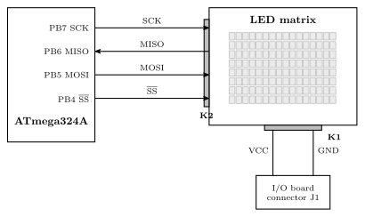
Figure 6: How the LED matrix is connected. Its SPI header K2 takes the four SPI pins of port B: the clock SCK, the data MOSI and the select line SS, which the AVR drives, and the data MISO coming back. Its power header K1 is fed from connector J1 on the I/O board, VCC on the left pin and GND on the right. The matrix only acts on bytes sent while SS is low.
The commands and the colour byte
Every message starts with a command byte. The two used here:
| Command | Bytes | Does |
|---|---|---|
| clear | 0x0F |
turns every pixel off |
| set one pixel | 0x01, position, colour |
sets the pixel at position to colour |
- The position byte is the row in the high nibble and the column in the low nibble:
(y << 4) | x, with x from 0 to 15 across and y from 0 to 7 up, (0, 0) being the bottom-left pixel. - The colour byte is the green brightness in the high nibble and the red brightness in the low nibble, each from 0 (off) to 15 (full):
(green << 4) | red. Mixing the two gives the colours between red and green.
| Colour byte | Green | Red | Colour |
|---|---|---|---|
0x00 |
0 | 0 | off (black) |
0x0F |
0 | 15 | red |
0x7F |
7 | 15 | orange |
0xFF |
15 | 15 | yellow |
0xF7 |
15 | 7 | chartreuse, a yellow-green |
0xF0 |
15 | 0 | green |
Worked: what colour is 0x7F?
What colour would a 0x7F colour data byte produce?
A. Red · B. Orange · C. Yellow · D. Chartreuse · E. Green · F. Black · G. Blue · H. Octarine
B, orange. 0x7F splits into a green nibble of 7 and a red nibble of 15: full red with about half as much green. Full red with full green, 0xFF, is yellow, so red with half the green sits between red and yellow, which is orange. Swapping the nibbles, 0xF7, gives chartreuse, the colour halfway from yellow to green. Blue is impossible on a matrix with only red and green LEDs, and octarine is a colour from fiction.
Worked: what do these bytes draw?
What would the LED matrix look like after receiving the bytes 0x0F, 0x01 0x24 0xF0, 0x01 0x46 0x0F? The six candidate pictures, A to F in Figure 7, each show one red and one green pixel, with each place given as (x, y): x across from the left and y up from the bottom, both counted from 0.
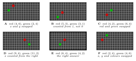
Figure 7: The six candidate pictures, each a 16 by 8 matrix with one red and one green pixel. E is what the bytes draw. Each of the others is the same two commands read with one slip, and the slip shows in where the pixels land. Reading the position byte’s nibbles the wrong way round swaps each pixel’s x and y (A). Counting x from the right mirrors the picture left to right (D). Counting from 1 instead of 0 moves every pixel one place down and one to the left (B). Reading the colour byte’s nibbles the wrong way round leaves the places alone but swaps the colours (C). F makes both swaps, A’s and C’s.
E. Split the bytes into commands:
0x0F: clear the display.0x01 0x24 0xF0: set one pixel. The position0x24is y = 2, x = 4, and the colour0xF0is green 15, red 0. Green at (4, 2).0x01 0x46 0x0F: set one pixel. Position0x46is y = 4, x = 6, colour0x0Fis red. Red at (6, 4).
Each wrong picture comes from one slip. A reads the position nibbles the wrong way round, taking 0x24 as x = 2, y = 4. C swaps the colour nibbles, so 0xF0 becomes red. F does both. D counts x from the right-hand edge, putting x = 4 in column 11 from the left. B counts from 1 instead of 0, so every pixel lands one column left and one row down.
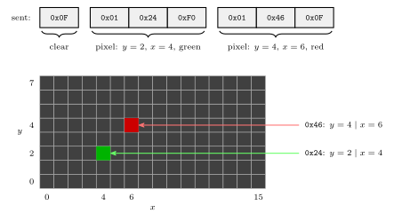
Figure 8: Seven bytes sent to the LED matrix, and what they draw. The stream divides into commands: 0x0F clears the display, and each 0x01 is followed by a position and a colour. A position byte holds y in its high nibble and x in its low nibble, so 0x24 is the pixel at x = 4, y = 2, counting from 0 at the bottom-left. A colour byte holds green in its high nibble and red in its low nibble, so 0xF0 is full green and 0x0F full red. Here red and green are the colours the LEDs show.
Worked: how fast does TCNT1 >> 8 count?
With a \(clk_{I/O}/1024\) prescaler, how quickly does TCNT1>>8 increment?
A. 7812 Hz · B. 3906 Hz · C. 1953 Hz · D. 976 Hz · E. 488 Hz · F. 244 Hz · G. 122 Hz · H. 61 Hz · I. 31 Hz · J. 15 Hz
I, 31 Hz. Timer/counter 1 counts at \(8\ \text{MHz} / 1024 = 7812.5\) counts a second. Shifting right by 8 throws away the bottom eight bits, so TCNT1>>8 goes up by one every \(2^8 = 256\) counts:
\[\frac{7812.5}{256} = 30.5\ \text{Hz}.\]
Each option is half the one before, and they line up with the shifts: A is TCNT1 itself, B is TCNT1>>1, and so on down to I for TCNT1>>8. TCNT1>>8 is the high byte of the count, 0 to 255, and it comes back round to 0 every \(65\,536 / 7812.5 = 8.4\) seconds (avr-timers-and-counters).
This is the timing the programs below use. Nothing has to be set up beyond the prescaler: the timer runs freely in normal mode, and a program that wants to do something every tenth of a second or so waits for TCNT1>>8 to move on by 3.
The tasks
- Joystick wiring test. Wire up the joystick and connect its two outputs to two LEDs on the I/O board. Wobble the stick: the LEDs’ brightness should change. Then unplug the LEDs, which upset the ADC readings if they are left connected.
- Joystick demo. Create a project with
lab16-1.c. Consult the datasheet and update the code as needed, then build and test it. - LED matrix demo. Create a project with
lab16-2.c. Consult the datasheet and update the code as needed, then build and test it. - Marquee. Needs two LED matrices, so work with someone else. Create a project with
lab16-3.c, which runs on one matrix as it is. Change it to drive two devices on the same MOSI, MISO and SCK pins but different SS pins. - Etch-A-Sketch. Create a project with
lab16-4.c: draw on the LED matrix with the joystick.
Working — Task 0
Join both + pins to VCC and one GND pin to GND. Run a wire from one L/R pin to LED L0 on the I/O board and one from a U/D pin to L1 (io-board). As the stick moves, each LED’s brightness follows the voltage on its axis, dim at one side and bright at the other. That shows both potentiometers are powered and both outputs move, before any code is involved.
Why the LEDs have to come off. A potentiometer’s wiper is a weak source. It sets the voltage, but it cannot supply current without that voltage changing. An LED draws current from it and pulls the voltage away from where the stick has put it, so the ADC would read the LED’s effect and not the stick’s position. The ADC input itself draws almost nothing.
Working — Task 1
lab16-1.c needs the converter’s register values from the datasheet. This is a complete program that does the job, to compare against. It reads both axes about ten times a second and prints them over the serial port, with the direction the stick is pushed. The serial set-up is the one from avr-usart.
#include <avr/io.h>
#include <stdint.h>

/* L/R (x) on PA0 = ADC0, U/D (y) on PA1 = ADC1.
   TXD0 (PD1) to the I/O board's serial receive, 9600 baud. */
#define X_CHANNEL 0
#define Y_CHANNEL 1

void adc_init(void) {
    ADMUX  = (1<<REFS0);                            /* AVCC, right adjusted, ADC0 */
    ADCSRA = (1<<ADEN) | (1<<ADPS2) | (1<<ADPS1);   /* on, clock = 8 MHz / 64     */
}

uint16_t adc_read(uint8_t channel) {
    ADMUX = (1<<REFS0) | channel;     /* for channel 1 this is 0x41        */
    ADCSRA |= (1<<ADSC);              /* start one conversion              */
    while (ADCSRA & (1<<ADSC)) { }    /* ADSC goes back to 0 when finished */
    return ADC;                       /* ADCL then ADCH: 0 to 1023         */
}

void uart_init(void) {
    UBRR0  = 51;                      /* 9600 baud                      */
    UCSR0B = (1<<TXEN0);              /* transmitter on; 8 data bits,   */
                                      /* no parity, 1 stop from reset   */
}

void uart_put(char c) {
    while (!(UCSR0A & (1<<UDRE0))) { }
    UDR0 = c;
}

void uart_print(const char *s) {
    while (*s) {
        uart_put(*s++);
    }
}

void uart_number(uint16_t n) {        /* four characters, right aligned */
    char d[4];
    int8_t i;

    for (i = 3; i >= 0; i--) {
        d[i] = '0' + n % 10;
        n /= 10;
    }
    for (i = 0; i < 3 && d[i] == '0'; i++) {
        d[i] = ' ';                   /* blank the leading zeros */
    }
    for (i = 0; i < 4; i++) {
        uart_put(d[i]);
    }
}

/* Which way the stick is pushed. Readings within 128 of the
   centre count as centred, so a stick at rest reads "centre". */
const char *direction(uint16_t x, uint16_t y) {
    static const char *name[3][3] = {
        /* x low        x middle    x high       */
        { "down-left", "down",     "down-right" },   /* y low    */
        { "left",      "centre",   "right"      },   /* y middle */
        { "up-left",   "up",       "up-right"   },   /* y high   */
    };
    uint8_t col = (x < 384) ? 0 : (x > 640) ? 2 : 1;
    uint8_t row = (y < 384) ? 0 : (y > 640) ? 2 : 1;
    return name[row][col];
}

int main(void) {
    uint16_t x, y;
    uint8_t now, last = 0;

    adc_init();
    uart_init();
    TCCR1A = 0;
    TCCR1B = (1<<CS12) | (1<<CS10);   /* timer 1 free running at 8 MHz / 1024 */

    while (1) {
        now = TCNT1 >> 8;                     /* advances 30.5 times a second */
        if ((uint8_t)(now - last) >= 3) {     /* so about 10 reports a second */
            last = now;
            x = adc_read(X_CHANNEL);
            y = adc_read(Y_CHANNEL);
            uart_print("x = ");
            uart_number(x);
            uart_print("   y = ");
            uart_number(y);
            uart_print("   ");
            uart_print(direction(x, y));
            uart_print("\r\n");
        }
    }
}
What each piece does.
adc_initsets the reference to AVCC and switches the converter on with its clock at 8 MHz / 64 = 125 kHz, the setting chosen above:ADPS2:0 = 110(analog-to-digital-conversion).adc_readselects the input, starts a conversion by settingADSC, and waits forADSCto drop back to 0, which the hardware does when the result is ready.REFS0is written again every time, because writingADMUXreplaces all eight bits.ADCis the 16-bit result register. The compiler reads its low byteADCLfirst and thenADCH, which is the order the hardware needs.- The pacing. Timer 1 runs freely at 8 MHz / 1024, so
TCNT1 >> 8goes up 30.5 times a second (worked above). A report goes out each time it has moved on by 3, about every 0.1 s. Subtracting asuint8_tkeeps the comparison right when the count wraps from 255 to 0. directionsorts each axis into low, middle or high with a margin of 128 either side of the centre, so that a stick at rest, which is never exactly at 511, readscentre.
Run on the joystick, it prints lines like
x =  511   y =  511   centre
x =  511   y =    0   down
x =  614   y =  689   up
x = 1023   y =  511   right
The reading (614, 689) comes out as up because its x is within the margin. At 60°, it is nearer straight up than the diagonal.
Working — Task 2
lab16-2.c needs the SPI register values from the datasheet. This program sets SPI up, sends the seven bytes decoded above, waits about two seconds, and then fills the matrix with every mix of red and green.
#include <avr/io.h>
#include <stdint.h>

#define CMD_PIXEL  0x01     /* then a position byte and a colour byte */
#define CMD_CLEAR  0x0F     /* every pixel off                         */

#define COLOUR(green, red)  (((green) << 4) | (red))    /* each 0 to 15 */

void spi_init(void) {
    DDRB  |= (1<<DDB7) | (1<<DDB5) | (1<<DDB4);   /* SCK, MOSI and SS out; MISO in */
    PORTB |= (1<<PORTB4);                          /* SS high to start with         */
    SPCR0  = (1<<SPE0) | (1<<MSTR0) | (1<<SPR10) | (1<<SPR00);   /* master, / 128  */
    /* SPI2X0 in SPSR0 stays 0 from reset */
    PORTB &= ~(1<<PORTB4);                         /* SS low: the matrix listens    */
}

uint8_t spi_send(uint8_t byte) {
    SPDR0 = byte;                       /* writing SPDR0 starts the transfer  */
    while (!(SPSR0 & (1<<SPIF0))) { }   /* SPIF0 is set after eight clocks    */
    return SPDR0;                       /* and reading SPDR0 next clears it   */
}

void matrix_clear(void) {
    spi_send(CMD_CLEAR);
}

void matrix_pixel(uint8_t x, uint8_t y, uint8_t colour) {
    spi_send(CMD_PIXEL);
    spi_send(((y & 0x07) << 4) | (x & 0x0F));   /* row high nibble, column low */
    spi_send(colour);
}

int main(void) {
    uint8_t x, y, start;

    spi_init();
    TCCR1A = 0;
    TCCR1B = (1<<CS12) | (1<<CS10);   /* 8 MHz / 1024 */

    /* the bytes 0x0F, 0x01 0x24 0xF0, 0x01 0x46 0x0F */
    matrix_clear();
    matrix_pixel(4, 2, COLOUR(15, 0));        /* green */
    matrix_pixel(6, 4, COLOUR(0, 15));        /* red   */

    start = TCNT1 >> 8;
    while ((uint8_t)((TCNT1 >> 8) - start) < 61) { }   /* about 2 seconds */

    /* every mix of the two colours: red grows to the right, green upwards */
    for (y = 0; y < 8; y++) {
        for (x = 0; x < 16; x++) {
            matrix_pixel(x, y, COLOUR(2 * y + 1, x));
        }
    }

    while (1) { }
}
Points to notice.
- Direction bits. In master mode the AVR drives SCK, MOSI and SS, so their
DDRBbits must be 1. MISO is made an input by the SPI hardware whatever itsDDRBbit says. - SS must be an output, or held high. If PB4 were an input and something pulled it low, the AVR would take that as another master claiming the bus, clear
MSTR0and drop out of master mode. As an output it is just a pin the program controls, here the matrix’s select line. spi_sendwaits onSPIF0. The flag is cleared by readingSPSR0while it is set and then readingSPDR0, which is what the loop and thereturndo. The byte returned is whatever the matrix shifted back, which these programs ignore.COLOUR(green, red)builds the colour byte from two brightnesses. The chart has red rising from 0 at the left to 15 at the right, and green from 1 at the bottom to 15 at the top. The bottom-right pixel is0x1F, nearly pure red, and the top-right is0xFF, yellow. The orange of0x7Fis at the right-hand end of row 3.- Speed. At 62.5 kHz a byte takes 128 µs, so the 128 pixel commands of the chart, 384 bytes, take about 49 ms.
Working — Task 3
Two matrices can share SCK, MOSI and MISO, because only the one whose \(\overline{\text{SS}}\) is low takes any notice of the bus. Each gets its own select line: the left matrix keeps PB4, and the right one is given PB3. The program selects a matrix, sends it complete commands, and selects the other. The two set-ups also need their grounds joined, since a signal on a wire only means something against a ground both ends share.
PB4 stays an output even when the right-hand matrix is the one selected, which keeps the AVR in master mode, for the reason given under Task 2.
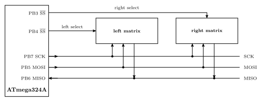
Figure 9: Two LED matrices on one SPI port. SCK, MOSI and MISO run to both, and a dot marks each real connection. Lines that cross without a dot are not connected. Each matrix has its own select line, PB4 for the left one and PB3 for the right one, and the program holds at most one of them low at a time. Only the selected matrix acts on the bytes on the bus. PB4 stays an output throughout, so the AVR stays the master.
The marquee. The message is laid out as a strip of columns: 32 blank ones, then each letter as five columns from a 5 by 7 font with one blank column after it. “CSSE2010” makes \(32 + 8 \times 6 = 80\) columns. The two matrices together are a window 32 columns wide onto the strip. At step \(s\) the left matrix shows columns \(s\) to \(s + 15\) and the right one \(s + 16\) to \(s + 31\). Each step moves the window one column to the right, which moves the text one column left, and after 80 steps the window is back at the start. The 32 blank columns let the text come in from the right-hand edge and go fully off the left before it starts again.
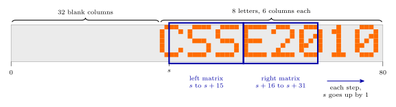
Figure 10: The marquee as a window sliding along a strip. The strip is 80 columns: 32 blank, so that the text can enter from the right, and then CSSE2010 in a 5 by 7 font with a blank column after each letter. At step s the left matrix shows columns s to s + 15 and the right matrix columns s + 16 to s + 31. Here s = 34. Each step adds 1 to s, and the text appears to move one column to the left.
#include <avr/io.h>
#include <stdint.h>

#define CMD_PIXEL  0x01
#define CMD_CLEAR  0x0F
#define COLOUR(green, red)  (((green) << 4) | (red))
#define TEXT       COLOUR(7, 15)            /* 0x7F, orange */

/* Both matrices are on SCK (PB7), MISO (PB6) and MOSI (PB5).
   Each has its own select line: the left one PB4, the right one PB3. */
#define SS_LEFT    PORTB4
#define SS_RIGHT   PORTB3

/* 5 x 7 letters, one byte per column, bit 0 the top row */
const char    letters[] = "CSE210 ";
const uint8_t font[][5] = {
    { 0x3E, 0x41, 0x41, 0x41, 0x22 },   /* C     */
    { 0x46, 0x49, 0x49, 0x49, 0x31 },   /* S     */
    { 0x7F, 0x49, 0x49, 0x49, 0x41 },   /* E     */
    { 0x42, 0x61, 0x51, 0x49, 0x46 },   /* 2     */
    { 0x00, 0x42, 0x7F, 0x40, 0x00 },   /* 1     */
    { 0x3E, 0x51, 0x49, 0x45, 0x3E },   /* 0     */
    { 0x00, 0x00, 0x00, 0x00, 0x00 },   /* space */
};

const char message[] = "CSSE2010";
#define MESSAGE_LENGTH  8
#define LEAD_IN         32                              /* blank columns first */
#define STRIP_LENGTH    (LEAD_IN + 6 * MESSAGE_LENGTH)  /* 80 columns          */

uint8_t shown[2][16];        /* the columns each matrix is showing now */

void spi_init(void) {
    DDRB  |= (1<<DDB7) | (1<<DDB5) | (1<<DDB4) | (1<<DDB3);
    PORTB |= (1<<SS_LEFT) | (1<<SS_RIGHT);       /* neither matrix selected */
    SPCR0  = (1<<SPE0) | (1<<MSTR0) | (1<<SPR10) | (1<<SPR00);
}

uint8_t spi_send(uint8_t byte) {
    SPDR0 = byte;
    while (!(SPSR0 & (1<<SPIF0))) { }
    return SPDR0;
}

void matrix_select(uint8_t m) {                  /* 0 = left, 1 = right */
    PORTB |= (1<<SS_LEFT) | (1<<SS_RIGHT);
    if (m == 0) {
        PORTB &= ~(1<<SS_LEFT);
    } else {
        PORTB &= ~(1<<SS_RIGHT);
    }
}

void matrix_pixel(uint8_t x, uint8_t y, uint8_t colour) {
    spi_send(CMD_PIXEL);
    spi_send(((y & 0x07) << 4) | (x & 0x0F));
    spi_send(colour);
}

/* Column i of the strip: 32 blank columns, then each letter
   as five columns and one blank column after it. */
uint8_t strip_column(uint8_t i) {
    uint8_t n, c, k;

    if (i < LEAD_IN) {
        return 0;
    }
    i -= LEAD_IN;
    n = i / 6;                        /* which letter of the message  */
    c = i % 6;                        /* which column of that letter  */
    if (c == 5) {
        return 0;                     /* the gap between letters      */
    }
    for (k = 0; letters[k] != message[n]; k++) { }
    return font[k][c];
}

/* Change column x of matrix m (already selected) to show bits,
   sending only the pixels that differ from what it shows now. */
void show_column(uint8_t m, uint8_t x, uint8_t bits) {
    uint8_t changed = bits ^ shown[m][x];
    uint8_t k;

    for (k = 0; k < 7; k++) {
        if (changed & (1<<k)) {
            matrix_pixel(x, 7 - k, (bits & (1<<k)) ? TEXT : 0x00);
        }
    }
    shown[m][x] = bits;
}

int main(void) {
    uint8_t step = 0, m, x, now, last;

    spi_init();
    TCCR1A = 0;
    TCCR1B = (1<<CS12) | (1<<CS10);         /* TCNT1 >> 8 counts at 30.5 Hz */

    for (m = 0; m < 2; m++) {
        matrix_select(m);
        spi_send(CMD_CLEAR);
    }

    last = TCNT1 >> 8;
    while (1) {
        now = TCNT1 >> 8;
        if ((uint8_t)(now - last) >= 3) {   /* one step about every 0.1 s */
            last = now;
            for (m = 0; m < 2; m++) {
                matrix_select(m);
                for (x = 0; x < 16; x++) {
                    show_column(m, x, strip_column((step + 16 * m + x) % STRIP_LENGTH));
                }
            }
            step = (step + 1) % STRIP_LENGTH;
        }
    }
}
How it works.
- The font. Each letter is five bytes, one per column, with bit 0 the top row. A row number \(k\) from the top becomes \(y = 7 - k\) on the matrix, so the letters fill rows 7 down to 1 and row 0 stays blank.
- Only changes are sent.
shownremembers what each column of each matrix is showing. XOR with the new column gives a 1 for every pixel that has to change, and only those get a command. Redrawing both matrices in full would be \(2 \times 128 \times 3 = 768\) bytes, about 0.1 s at 128 µs a byte, which would use up the whole step. Sending only the changes is a few dozen pixels a step. - Selecting.
matrix_selectraises both select lines and then lowers one, so the two are never low together, and it is only called between complete commands. A matrix deselected halfway through a command would be left waiting for the rest of it. - The pace is three counts of
TCNT1 >> 8, \(3 \times 256 / 7812.5 = 98\) ms a step, so the 80-step cycle takes just under 8 seconds.
Working — Task 4
The Etch-A-Sketch has a pen, a red pixel that blinks, and the stick moves it one pixel at a time. Wherever the pen has been is left green. A push of button B0 on the I/O board, wired to PD2, wipes the drawing.
#include <avr/io.h>
#include <stdint.h>

#define CMD_PIXEL  0x01
#define CMD_CLEAR  0x0F
#define COLOUR(green, red)  (((green) << 4) | (red))
#define TRAIL      COLOUR(15, 0)     /* green: the line drawn */
#define PEN        COLOUR(0, 15)     /* red: where the pen is */
#define BLANK      0x00

/* Joystick x on PA0 (ADC0), y on PA1 (ADC1). LED matrix on PB7 to PB4.
   Push button B0 on PD2 clears the drawing. */

uint8_t drawn[16];           /* bit y of drawn[x] is 1 where the line has been */

void adc_init(void) {
    ADMUX  = (1<<REFS0);
    ADCSRA = (1<<ADEN) | (1<<ADPS2) | (1<<ADPS1);
}

uint16_t adc_read(uint8_t channel) {
    ADMUX = (1<<REFS0) | channel;
    ADCSRA |= (1<<ADSC);
    while (ADCSRA & (1<<ADSC)) { }
    return ADC;
}

void spi_init(void) {
    DDRB  |= (1<<DDB7) | (1<<DDB5) | (1<<DDB4);
    PORTB |= (1<<PORTB4);
    SPCR0  = (1<<SPE0) | (1<<MSTR0) | (1<<SPR10) | (1<<SPR00);
    PORTB &= ~(1<<PORTB4);
}

uint8_t spi_send(uint8_t byte) {
    SPDR0 = byte;
    while (!(SPSR0 & (1<<SPIF0))) { }
    return SPDR0;
}

void matrix_pixel(uint8_t x, uint8_t y, uint8_t colour) {
    spi_send(CMD_PIXEL);
    spi_send(((y & 0x07) << 4) | (x & 0x0F));
    spi_send(colour);
}

void clear_drawing(void) {
    uint8_t x;

    spi_send(CMD_CLEAR);
    for (x = 0; x < 16; x++) {
        drawn[x] = 0;
    }
}

/* -1, 0 or +1 for one axis: it has to be pushed past half way */
int8_t step_for(uint16_t reading) {
    if (reading < 256) {
        return -1;
    }
    if (reading > 767) {
        return 1;
    }
    return 0;
}

int main(void) {
    uint8_t x = 8, y = 4;                /* the pen starts in the middle */
    int8_t nx, ny;
    uint8_t now, last_move, blink, shown_blink = 2;
    uint8_t button, last_button = 0;

    adc_init();
    spi_init();
    DDRD &= ~(1<<DDD2);                  /* the clear button is an input */
    TCCR1A = 0;
    TCCR1B = (1<<CS12) | (1<<CS10);      /* 8 MHz / 1024 */

    clear_drawing();
    last_move = TCNT1 >> 8;

    while (1) {
        /* clear on the push of the button, not for as long as it is held */
        button = (PIND >> PIND2) & 1;
        if (button && !last_button) {
            clear_drawing();
            shown_blink = 2;             /* make the pen be drawn again */
        }
        last_button = button;

        /* move at most one pixel every 4 counts of TCNT1 >> 8: 7.6 a second */
        now = TCNT1 >> 8;
        if ((uint8_t)(now - last_move) >= 4) {
            last_move = now;
            nx = x + step_for(adc_read(0));
            ny = y + step_for(adc_read(1));
            if (nx < 0)  { nx = 0; }
            if (nx > 15) { nx = 15; }
            if (ny < 0)  { ny = 0; }
            if (ny > 7)  { ny = 7; }
            if (nx != x || ny != y) {
                drawn[x] |= (1<<y);          /* leave the line where the pen was */
                matrix_pixel(x, y, TRAIL);
                x = nx;
                y = ny;
                shown_blink = 2;
            }
        }

        /* the pen blinks: bit 12 of TCNT1 flips every 4096 counts, 0.52 s */
        blink = (TCNT1 >> 12) & 1;
        if (blink != shown_blink) {
            if (blink) {
                matrix_pixel(x, y, PEN);
            } else {
                matrix_pixel(x, y, (drawn[x] & (1<<y)) ? TRAIL : BLANK);
            }
            shown_blink = blink;
        }
    }
}
How it works.
- Reading the stick as a step.
step_forturns a reading into \(-1\), 0 or \(+1\), with the stick pushed past half way, below 256 or above 767, before it counts. Both axes are read each time, so a diagonal push moves the pen diagonally. - Pacing from the timer. The pen moves at most once per 4 counts of
TCNT1 >> 8, which is \(4 \times 256 / 7812.5 = 131\) ms, about 7.6 moves a second. Without it the pen would cross the matrix in a few milliseconds. - Blinking from the timer. Bit 12 of
TCNT1changes every \(2^{12} = 4096\) counts, 0.52 s, so(TCNT1 >> 12) & 1is a square wave with a period of just over a second, for nothing more than a read of the count. The pixel is only resent when that bit changes, not on every pass of the loop. - Remembering the drawing.
drawnholds one bit per pixel, so that when the pen blinks off it shows the line underneath, or nothing, as it should. shown_blink = 2is a value the bit can never have, which forces the pen to be redrawn on the next pass after a move or a clear.- The button clears on its rising edge, the moment it goes down, using the same comparison with the previous reading as the stopwatch in week9-lab-avr-interrupts.
Which way is up. The program moves the pen in the joystick’s own frame: right with x, up with y. Set in the breadboard as described above, the joystick’s x points to the top of the breadboard (Figure 3), so pushing the stick away moves the pen right. To have the pen follow the stick as seen from in front of the breadboard, swap the axes and reverse one: move right as y falls and up as x rises, which is nx = x - step_for(adc_read(1)) and ny = y + step_for(adc_read(0)).
See also
- analog-to-digital-conversion — the converter’s registers, its clock, a conversion step by step
- avr-spi — the SPI bus, its registers and the shift-register ring
- io-board — the joystick’s pins and the LED matrix’s commands
- avr-timers-and-counters — the prescaler and the slow count from
TCNT1 >> 8 - avr-usart — the serial port Task 1 prints through
- polling-and-interrupts — the two ways to wait for a conversion or a transfer
- week9-lab-avr-interrupts — Lab 14
- 2026-09-24-serial-io — Lecture 18 · 2026-10-05-more-io — Lecture 19