Analog to Digital Conversion
Turning a voltage into a number the processor can use. A digital input pin only distinguishes 0 from 1. An analog to digital converter (ADC) reports how big a voltage is, to a fixed number of bits. First met in 2026-09-24-serial-io, and used to read a joystick in week10-lab-adc-and-spi.
What a converter does
An ADC takes an input voltage between 0 and a maximum, the reference voltage \(V_{ref}\), and produces an unsigned integer in proportion to it. Zero volts gives 0, and a voltage just under \(V_{ref}\) gives the largest value the result can hold.
The number of bits in the result is the converter’s resolution. With \(n\) bits there are \(2^n\) possible results, 0 to \(2^n - 1\):
| Resolution | Results | Range |
|---|---|---|
| 8 bits | 256 | 0 to 255 |
| 10 bits | 1024 | 0 to 1023 |
| 12 bits | 4096 | 0 to 4095 |
From voltage to number
The converter divides the range from 0 to \(V_{ref}\) into \(2^n\) equal steps and reports which step the input is on. For a 10-bit converter:
\[\text{result} = \left\lfloor \frac{V_{in}}{V_{ref}} \times 1024 \right\rfloor, \qquad \text{at most } 1023\]
and the size of one step is
\[\frac{V_{ref}}{1024} = \frac{5\ \text{V}}{1024} \approx 4.9\ \text{mV} \quad\text{when } V_{ref} = 5\ \text{V}.\]
| \(V_{in}\) (with \(V_{ref}\) = 5 V) | Result |
|---|---|
| 0 V | 0 |
| 1.25 V | 256 |
| 2.5 V | 512 |
| 3.75 V | 768 |
| 5 V | 1023 |
Two things follow from the staircase in Figure 1.
- The result is rounded down to a step. Every voltage within one step gives the same number, so a result is only known to within one step, 4.9 mV here. More bits means smaller steps.
- The top result is \(2^n - 1\), not \(2^n\). There are 1024 steps numbered from 0, so full scale reads 1023.
Going the other way, a result \(r\) stands for a voltage of about \(r \times V_{ref} / 1024\). A reading of 300 with a 5 V reference is about \(300 \times 4.88\ \text{mV} = 1.46\ \text{V}\).
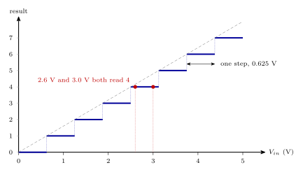
Figure 1: Conversion with a 3-bit converter and a 5 V reference, drawn with few enough steps to see. The input range is cut into \(2^3 = 8\) equal steps of 0.625 V, and the result is the number of the step the input is on, from 0 to 7. Every voltage within a step gives the same result, so 2.6 V and 3.0 V both read 4. A 10-bit converter does the same thing with 1024 steps of about 4.9 mV.
The ATmega324A’s converter
- Inputs. The eight port A pins can be used as analog inputs. A pin used this way is not read through
PINA. The result comes from the converter’s own data register,ADC, which is 16 bits wide to hold the 10-bit result. - One at a time. There is a single converter, with an analog multiplexer in front of it that connects one of the pins to it. To read two voltages, such as the two axes of a joystick, select one pin and convert, then select the other and convert.
- Reference. \(V_{ref}\) can be chosen. The course uses the supply, \(V_{cc} = 5\ \text{V}\).
- Resolution. 10 bits: results from 0 to 1023.
- Time. A conversion is not instant. It takes up to 3200 clock cycles, which is 0.4 ms with the 8 MHz clock. The converter can be run faster at the cost of accuracy.
Because a conversion takes thousands of clock cycles, starting one and getting the answer are separate moments. Between them the program either waits and checks whether the converter has finished, or does something else and lets the converter raise an interrupt when it has (polling-and-interrupts). The interrupt has its own vector, written ISR(ADC_vect) in C (avr-interrupts).
Worked: a joystick
A joystick gives two voltages between 0 and 5 V, one for left-right and one for up-down. Pushed three-quarters of the way right and a quarter of the way up, it gives 3.75 V and 1.25 V, which convert to 768 and 256. Centred, each axis is near 2.5 V and reads near 512. Each reading takes its own conversion, so the two numbers are from slightly different moments.
Inside, each axis is a potentiometer between 5 V and ground, and the stick moves its wiper, so the wiper’s voltage follows the stick from one side to the other (io-board).
Worked: where is the stick?
A joystick’s reading is easiest to interpret measured from the centre. Half of 1023 is 511.5, so 511 and 512 do equally well as the centre. Taking 511 on both axes,
\[\Delta x = x - 511, \qquad \Delta y = y - 511,\]
the direction of the stick is the angle \(\tan^{-1}(\Delta y / \Delta x)\), measured anticlockwise from straight right and put in the right quadrant by the signs, and how far it is pushed is \(\sqrt{\Delta x^2 + \Delta y^2} / 511\) of full deflection.
- (511, 0): \(\Delta x = 0\), \(\Delta y = -511\). Straight down, all the way.
- (614, 689): \(\Delta x = 103\), \(\Delta y = 178\). The angle is \(\tan^{-1}(178/103) = 60^\circ\), and the distance is \(\sqrt{103^2 + 178^2} = 206\), which is \(206 / 511 = 40\,\%\) of full deflection.
The readings themselves are never negative: \(\Delta x\) and \(\Delta y\) are what a program works out, not what the converter reports. And the centre is only roughly 511, since a real stick at rest sits a few counts to one side, so a program tests against a margin, as in week10-lab-adc-and-spi.
The registers
A program runs the converter through three registers, counting the 16-bit result as one:
| Register | Holds |
|---|---|
ADMUX |
which reference, which input, and how the result is lined up |
ADCSRA |
on and off, start, the finished flag and its interrupt enable, and the clock prescaler |
ADC, as ADCH and ADCL |
the result |
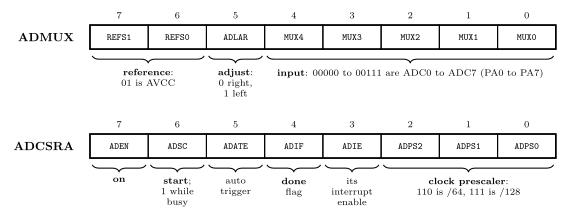
Figure 2: The converter’s two control registers, with their bits grouped by what they do. In ADMUX the top two bits choose the reference voltage, bit 5 chooses whether the 10-bit result is lined up at the right or the left of its 16-bit register, and the bottom five choose the input pin. In ADCSRA bit 7 switches the converter on, bit 6 starts a conversion and stays 1 while it runs, bit 4 is the flag set when a result is ready and bit 3 its interrupt enable, and the bottom three bits divide the system clock down to the converter’s own clock.
ADMUX: what to convert
REFS1 |
REFS0 |
Reference voltage |
|---|---|---|
| 0 | 0 | whatever is on the AREF pin |
| 0 | 1 | AVCC, the converter’s supply, 5 V on the lab boards |
| 1 | 0 | an internal 1.1 V |
| 1 | 1 | an internal 2.56 V |
ADLAR, ADC left adjust result, is 0 for a result lined up at the right of the 16-bit register, so that it reads as a number from 0 to 1023. Set to 1, it is lined up at the left instead (below).MUX4:0picks the input.00000to00111are the pins ADC0 to ADC7, which are PA0 to PA7, each on its own. The other codes select differential pairs of pins and two internal test voltages, which the course does not use.
Worked: the value for ADC1
AVCC as the reference, right adjusted, input ADC1:
\[\underbrace{01}_{\texttt{REFS1:0}}\ \underbrace{0}_{\texttt{ADLAR}}\ \underbrace{00001}_{\texttt{MUX4:0}} = \texttt{0100 0001} = \texttt{0x41}\]
In C, ADMUX = (1<<REFS0) | 1;. Writing the register replaces all eight bits, so the reference bits have to be included every time the input is changed. ADMUX = 1; alone would select ADC1 with the AREF pin as the reference, which on a board with nothing connected to AREF gives meaningless results.
ADCSRA: control and status
| Bit | Name | |
|---|---|---|
| 7 | ADEN |
enable: 1 switches the converter on. Nothing happens without it |
| 6 | ADSC |
start conversion: write a 1 to start one. It reads 1 while the conversion runs and drops to 0 when the result is ready |
| 5 | ADATE |
auto trigger: start conversions automatically, for example one after another. Left 0 here |
| 4 | ADIF |
interrupt flag: set when a conversion finishes. Cleared by writing a 1 to it, or by the hardware when the interrupt is taken |
| 3 | ADIE |
interrupt enable for that flag |
| 2–0 | ADPS2:0 |
prescaler: what the system clock is divided by to make the ADC clock |
ADPS2:0 |
000 | 001 | 010 | 011 | 100 | 101 | 110 | 111 |
|---|---|---|---|---|---|---|---|---|
| Divide by | 2 | 2 | 4 | 8 | 16 | 32 | 64 | 128 |
| ADC clock at 8 MHz | 4 MHz | 4 MHz | 2 MHz | 1 MHz | 500 kHz | 250 kHz | 125 kHz | 62.5 kHz |
ADEN and the prescaler are set once. ADSC is set for every conversion.
The result: ADCH and ADCL
The 10-bit result sits in a 16-bit register made of two bytes, ADCH and ADCL. ADLAR decides where.
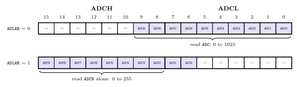
Figure 3: Where the 10 result bits go in ADCH:ADCL. Right adjusted, with ADLAR = 0, bits 9 and 8 are the bottom two bits of ADCH and the rest fill ADCL, so the 16-bit register reads as a number from 0 to 1023 and the six unused bits are 0. Left adjusted, with ADLAR = 1, the result starts at the top, so ADCH on its own holds the top 8 bits, a result from 0 to 255 for a program that does not need all 10.
- Read the low byte first. Reading
ADCLlocks the register, so that a conversion finishing in between cannot replace one byte and not the other, and readingADCHunlocks it. The order isADCL, thenADCH. - In C, read
ADC. The header definesADCas the 16-bit register, and the compiler reads the two bytes in the right order. - Left adjusted,
ADCHalone will do. WithADLAR= 1 the top 8 bits are all inADCH, and readingADCHby itself is allowed. It gives an 8-bit result, steps of about 20 mV with a 5 V reference.
The ADC clock
The converter has its own clock, made by dividing the system clock with the prescaler in ADCSRA. For the full 10 bits of precision, the ADC clock must be between 50 kHz and 200 kHz. A faster clock gives a quicker conversion with fewer accurate bits, which is the trade between accuracy and speed.
A conversion takes 13 ADC clock cycles. The first one after ADEN is set takes 25, because the analog circuits have to settle. At the slowest setting, the system clock divided by 128, that first conversion is \(25 \times 128 = 3200\) system clock cycles, 0.4 ms at 8 MHz, which is the “up to 3200 clock cycles” above.
Worked: choosing the prescaler
With the 8 MHz system clock, the ADC clock is \(8\ \text{MHz} / N\). For it to lie between 50 and 200 kHz,
\[\frac{8\ \text{MHz}}{200\ \text{kHz}} \le N \le \frac{8\ \text{MHz}}{50\ \text{kHz}} \quad\Longrightarrow\quad 40 \le N \le 160.\]
Of the settings on offer, 64 (125 kHz) and 128 (62.5 kHz) are in range. Either is right. 64 is the faster of the two: a conversion takes \(13 \times 64 = 832\) system cycles, 104 µs.
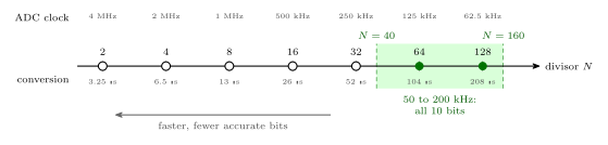
Figure 4: The prescaler settings against the window for full precision. Each setting divides the 8 MHz system clock, giving the ADC clock above the axis and the time for one 13-cycle conversion below it. Only the shaded band, an ADC clock from 50 to 200 kHz, gives all 10 bits. That band is a divisor from 40 to 160, and the two settings inside it are 64 and 128. Settings to the left are faster but less accurate.
A conversion, step by step
- Choose the reference and the input in
ADMUX. - Switch on the converter and set its clock:
ADENand the prescaler bits inADCSRA. Once is enough. - Start a conversion by setting
ADSC. - Wait until it has finished.
ADSCreads 1 until then, and at the end the hardware clears it and setsADIF. - Read the result from
ADC.
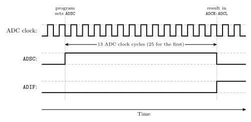
Figure 5: One conversion against time. The program writes a 1 to ADSC and the conversion starts. ADSC stays at 1 for the 13 cycles of the ADC clock that the conversion takes, 25 for the first one after the converter is switched on. At the end the hardware puts ADSC back to 0, sets the flag ADIF and leaves the new result in ADCH:ADCL. A program can wait for either bit, or enable the interrupt and be told.
By polling. Wait for ADSC to drop:
#include <avr/io.h>
#include <stdint.h>

uint16_t adc_read(uint8_t channel) {
    ADMUX = (1<<REFS0) | channel;     /* AVCC, right adjusted, this input */
    ADCSRA |= (1<<ADSC);              /* start                             */
    while (ADCSRA & (1<<ADSC)) { }    /* busy while ADSC reads 1           */
    return ADC;                       /* ADCL, then ADCH                   */
}

int main(void) {
    uint16_t x, y;

    ADCSRA = (1<<ADEN) | (1<<ADPS2) | (1<<ADPS1);   /* on, 8 MHz / 64 = 125 kHz */
    while (1) {
        x = adc_read(0);
        y = adc_read(1);
        (void)x; (void)y;
    }
}
Waiting on ADSC needs no clearing up afterwards. Waiting on ADIF works too, but the flag stays set until a 1 is written to it, so the program has to clear it before the next conversion.
By interrupt. Set ADIE and write a handler for ADC_vect (avr-interrupts). The handler here collects each result and starts the next conversion, so the converter runs continuously and the main program reads the latest value whenever it wants one:
#include <avr/io.h>
#include <avr/interrupt.h>
#include <stdint.h>

volatile uint16_t latest;             /* the newest result */

ISR(ADC_vect) {
    latest = ADC;                     /* ADIF is cleared as the handler starts */
    ADCSRA |= (1<<ADSC);              /* start the next conversion             */
}

int main(void) {
    uint16_t x;

    ADMUX  = (1<<REFS0);                                      /* AVCC, ADC0 */
    ADCSRA = (1<<ADEN) | (1<<ADIE) | (1<<ADPS2) | (1<<ADPS1); /* / 64       */
    sei();
    ADCSRA |= (1<<ADSC);              /* the first conversion */

    while (1) {
        cli();                        /* a 16-bit copy must not be split */
        x = latest;
        sei();
        /* ... use x ... */
        (void)x;
    }
}
latest is two bytes, so the main program copies it with interrupts off, for the reason in software-timers.
Changing input. A change to ADMUX during a conversion only takes effect when that conversion has finished. Change the input between conversions, as adc_read does.
Common mistakes
- Expecting 1024 at full scale. The largest 10-bit result is 1023.
- Forgetting the reference. The same result means a different voltage with a different \(V_{ref}\). A result is a fraction of the reference.
- Treating the result as exact. It is the step the voltage was on, good to one step.
- Expecting two inputs to be read together. One converter, one input at a time.
- Using the result the instant a conversion is started. It is not ready for up to 0.4 ms.
- Forgetting
ADEN. SettingADSCon a converter that is switched off starts nothing. - Losing the reference bits.
ADMUX = 1;selects ADC1 but also setsREFS1:0to00, the AREF pin. Keep(1<<REFS0)in every write. - A prescaler outside the window. At 8 MHz only 64 and 128 put the ADC clock between 50 and 200 kHz. Anything faster gives fewer good bits.
- Reading
ADCHbeforeADCL. ReadingADCLlocks the result untilADCHis read. Read the 16-bitADCin C and the order is right. - Expecting negative readings. The result is unsigned, 0 to 1023. A joystick’s offset from its centre is something the program works out by subtracting.
- Loading the input. An LED, or the pin’s own pull-up resistor switched on through
PORTA, draws current from the voltage being measured and changes it. A potentiometer’s wiper in particular cannot supply current without its voltage moving.
See also
- 2026-09-24-serial-io — Lecture 18, where the converter is introduced
- week10-lab-adc-and-spi — Lab 16: the prescaler and
ADMUXworked, reading a joystick, and four programs that use it - io-board — the joystick module and its pins
- avr-io-ports — the digital side of the same pins
- polling-and-interrupts · avr-interrupts — the two ways to find out a conversion has finished
- avr-architecture — the A/D converter on the block diagram
- binary-number-representations — unsigned integers, and why 10 bits hold 0 to 1023