The I/O Board
The I/O board in the lab kit carries the input and output devices you wire your breadboard circuits to, for experimenting with simple digital circuits. It plugs directly onto the breadboard, and adds a logic probe for debugging and a UART serial interface for talking to other devices.
It is powered from a single USB connection and has current-sense circuitry that detects short circuits and protects your designs.
Pin numbers for every device are in device-pinouts; the kit itself is loaned out in week3-lab-logisim-and-flip-flops. Two more parts of the kit that are used alongside the board, the joystick and the LED matrix, are described at the end.
What’s on it
| 1. USB connector | 2. Power LED | 3. Power switch | 4. 7-segment display |
| 5. Switches | 6. LEDs | 7. Buttons | 8. UART transmit/receive LEDs |
| 9. Logic probe indicator LEDs | 10. Fault LED | 11. VCC / GND headers | 12. I/O device headers |
| 13. Auxiliary power connector | 14. High current mode jumper |
Items 13 and 14 are the auxiliary power connector and the high-current-mode jumper. The one extra power connection the labs use is connector J1, which powers the LED matrix in Lab 16 (below).
The board at a glance
The board is a C shape: a left-hand spine carrying the USB connector, the power switch, the two status LEDs and the seven-segment display, plus a top arm and a bottom arm that straddle the breadboard’s central channel. All the I/O devices come out on the two 16-pin headers on the inner edges of those arms, and every device is reached through the column of breadboard holes directly above or below its printed label.
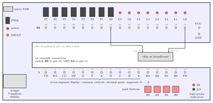
Figure 1: A plan view of the board, not to scale, with the parts on the left spine placed roughly. Each I/O device sits on one pin of one of the two 16-pin headers, and the column of breadboard holes at that pin is how you reach it. The board itself prints only the two end markers, a bold 32 at the left of the top header and a bold 1 at the left of the bottom one. The small numbers at the other pins are their pin numbers, the ones a schematic uses. The connection drawn in the notch is an example: switch S0 to pin 13 of a chip, LED L0 to pin 11.
Two things about the numbering are worth fixing in your head before you wire anything:
- The top header counts down, left to right. Its leftmost pin is 32 and its rightmost is 17, so the switches run
S7…S0and then the LEDsL7…L0as you read left to right. That is the opposite of the reading order you would guess from the pin numbers alone. - The bottom header counts up, left to right, pin 1 to pin 16:
TX RX CC DP G F E D C B A B3 B2 B1 B0 PR. The middle nine of those are the seven-segment display —CCits common cathode,DPits decimal point, andGdown toAits seven segments — which is why nine consecutive pins carry single-letter names.
VCC and GND pads sit at the far right of both arms, which is where the breadboard’s power rails get fed from.
Setup
Insert the board into the breadboard, aligning the downward-facing headers with the right holes.
If aligned correctly, the I/O board should not require excessive force to insert.
Connect a micro-USB cable to the connector at the top-left corner.
DO NOT STORE THE BOARD WITH THE USB CABLE ATTACHED — THIS MAY CAUSE THE USB CONNECTOR TO BREAK OFF!!
The USB connector is the part people break.
Turn the board on by sliding the PWR switch up to ON; the red power LED should light. Then check the orange FAULT LED does not light. If it does, power off immediately.
The fault LED
The board uses a current-limited power switch to protect itself and anything it powers from short circuits. A short lights the orange FAULT LED.
If it’s on: push PWR down to OFF immediately, and check your design for shorts before restoring power.
WARNING! In the case of a short circuit, the current-limiting switch may become extremely hot.
The logic probe
Attach a wire to the column of terminals above the PR label — pin 16, the rightmost pin of the bottom header. Touch the free end to any point in the circuit and the HI / LO LEDs show the logic state there.
As circuits increase in complexity, so does the necessity of having a clear strategy — probing random points in a large circuit rarely reveals the location of errors.
Suggested troubleshooting strategy
- Check the FAULT light is not on, which would indicate a short circuit.
- Probe VCC and GND at every device in your circuit, to confirm each one is actually powered.
- Start at the inputs and move logically through to the outputs. Pen and paper helps: write down the expected state at each point first, then verify it with the probe. A schematic and a truth table are great for this.
The key to any successful debugging strategy is to assume nothing, know what to expect before you begin testing, and have a plan.
Step 2 is the one worth internalising — an unpowered chip looks exactly like a wrong-logic chip until you probe its power pins, and grouped VCC/GND entries on a schematic (see circuit-schematics) make it easy to forget one.
Electrical characteristics
| VCC | 5 V |
| GND | 0 V |
| Logic high | > 3.5 V |
| Logic low | < 1.5 V |
The gap between 1.5 V and 3.5 V is undefined, which is why a floating pin can read as either (week3-lab-logisim-and-flip-flops). What the logic probe shows for a voltage inside that band is not documented.
The joystick
The kit’s two-axis joystick is a small board of its own, made to sit in the breadboard next to the I/O board. Each axis is a potentiometer between its own supply pin and ground, and the stick moves the wiper. So each axis gives a voltage that follows the stick across its travel, from 0 V at one side to 5 V at the other, for the A/D converter to read (analog-to-digital-conversion).
| Pin | What it is | Connect to |
|---|---|---|
| L/R+ | top of the left-right potentiometer | VCC |
| U/D+ | top of the up-down potentiometer | VCC |
| GND ×2 | bottom of both | GND, either one |
| L/R ×2 | x: 0 V with the stick to the left, 5 V to the right | an analog input, either one |
| U/D ×2 | y: 0 V at the bottom, 5 V at the top | an analog input, either one |
- The doubled pins are joined on the board. One wire to each of L/R, U/D and GND is enough.
- The two
+pins are separate. Both have to go to VCC, or one axis has nothing to divide. - Left, right, up and down are the joystick’s own, marked by the X and Y arrows printed on it. Placed at the right-hand end of the breadboard, with room for the microcontroller board and programmer to its left, the X arrow points to the top of the breadboard and the Y arrow to the left.
- A potentiometer’s wiper is a weak source. Anything that draws current from it, an LED for instance, pulls its voltage away from the stick’s position. LEDs make a quick wiring test, but they must come off before the converter is used.
- Keep the black foam that protects the pins when the joystick is put away.
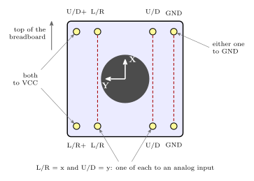
Figure 2: The joystick’s eight pins, seen from above with the board placed as it sits in the breadboard, its X arrow pointing to the top. The pins near each corner come in twos. The dashed lines join the pins that are connected on the board itself: the two L/R pins, the two U/D pins and the two GND pins, so one wire to each pair is enough. The two supply pins, U/D+ at the top left and L/R+ at the bottom left, are not joined, and both go to VCC. L/R carries x and U/D carries y to the analog inputs.
The LED matrix
The LED matrix is a display of 16 columns by 8 rows, each pixel a red LED and a green LED together. It is driven over SPI: the AVR is the master and the matrix a slave that takes commands one byte at a time (avr-spi).
Connecting it
It has two headers:
- K1, two pins, is its power. A two-wire lead joins it to the I/O board’s connector J1, VCC on J1’s left pin and GND on its right.
- K2, four pins, is the SPI connection, to the AVR’s SPI port on PB7 to PB4: SCK on PB7, MISO on PB6, MOSI on PB5 and \(\overline{\text{SS}}\) on PB4. Match the order of the pins on K2 against the datasheet before plugging the lead in.
The Err state. PB7 to PB5 are also the pins the programmer uses to load the AVR, so programming sends the matrix a stream of what look to it like garbage commands, and it can show Err. Holding the AVR’s reset button down for at least half a second after programming clears it before the program starts.
What to send it
Every message starts with a command byte. Two commands are enough to draw anything:
| Command | Bytes | Does |
|---|---|---|
| clear | 0x0F |
every pixel off |
| set one pixel | 0x01, position, colour |
sets one pixel to a colour |
- Position byte:
(y << 4) | x. The row y, from 0 at the bottom to 7 at the top, is the high nibble. The column x, from 0 at the left to 15 at the right, is the low nibble. - Colour byte:
(green << 4) | red. Each nibble is a brightness from 0 to 15. Red alone is0x0F, green alone0xF0, both full is yellow,0xFF, and full red with half green is orange,0x7F.
The matrix’s reference manual is the full description of the commands it accepts.
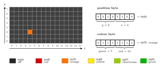
Figure 3: How a pixel is addressed and coloured. The matrix is 16 columns, x from 0 to 15 left to right, by 8 rows, y from 0 to 7 bottom to top. A position byte puts y in its high nibble and x in its low one, so the pixel at x = 4, y = 2 is 0x24. A colour byte puts the green brightness in its high nibble and the red in its low one, each 0 to 15. The swatches show what some colour bytes look like: the colours here are the light from the red and green LEDs mixed.
Lab 16 works through the commands and uses them for a demo, a scrolling marquee across two matrices and an Etch-A-Sketch (week10-lab-adc-and-spi).
See also
- device-pinouts — the pin table behind Figure 1, and the board’s schematic symbols
- circuit-schematics — how the board is drawn on a schematic (
IO1/IOBOARD, input and output pentagons) - avr-io-ports — the same switches and LEDs driven from an AVR rather than from gates
- week3-lab-logisim-and-flip-flops — where the kit is loaned out
- week10-lab-adc-and-spi — Lab 16: the joystick read by the A/D converter, and the LED matrix driven over SPI
- analog-to-digital-conversion · avr-spi — the two AVR peripherals the joystick and the matrix are used with