Logisim and Flip-Flops
Learning Lab 5 — verify the operation of latches and the D flip-flop in Logisim, then build one. It is also the session where kits are loaned out. Pairs with 2026-08-10-introduction-to-sequential-circuits and flip-flops-and-latches.
Recall
There are two types of logic circuit: combinational and sequential. The basic building block of sequential circuits is the flip-flop, which stores 1 bit of information. See flip-flops-and-latches and sequential-circuits.
Worked: which is NOT a combinational circuit?
A counter. Adders, multiplexers, decoders and adder/subtractors are all combinational — their output is a function of the current inputs alone, and every one of them appeared in Lab 4 (see week3-lab-lab-4-pre-work). A counter has to remember where it is, so it is sequential. See counters.
Worked: which waveform captures the behaviour of this circuit?
The circuit is a rising-edge-triggered D flip-flop (a wedge on the clock input with no bubble in front of it) with \(A\) on \(D\), \(CLK\) on the clock, and \(Q\) taken out. SET and CLR are lettered inside the box but not driven.
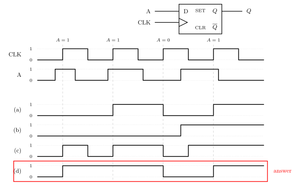
Figure 1: The circuit, its two input waveforms CLK and A, and the four candidate outputs. The answer is (d). The dashed verticals through the four rising clock edges, and the A = 1/1/0/1 labels above them, are what makes the answer mechanical, since a rising-edge flip-flop copies D to Q at those four instants and nowhere else.
Answer: (d). Sample \(A\) at each rising edge of \(CLK\) and nowhere else: the values are 1, 1, 0, 1, so \(Q\) goes high at the first edge, holds through the second, drops at the third and rises again at the fourth. Between edges \(Q\) does nothing at all, however much \(A\) moves.
The three wrong waveforms each fail in a different, recognisable way:
- (a) agrees with (d) from the second clock edge onwards but misses the first. \(A\) is already high when the first edge arrives, so the flip-flop does capture it — this is the answer you get by mentally starting one edge late.
- (b) changes exactly once, at the moment \(A\) last rises. That is a wire, not a flip-flop: no clock edge is involved.
- (c) changes at instants where the clock is falling as well as where it is rising, which no single-edge-triggered device does.
Worked: which of these is FALSE about a negative-edge-triggered D flip-flop?
“Changes on the D input affect the output when the clock signal is at logic 0.”
That describes a level-triggered latch — the thing an edge-triggered flip-flop is defined in contrast to. An edge-triggered device responds only at the transition; for a negative-edge part, when the clock goes 1 → 0. The other three statements (stores 1 bit, is a sequential circuit, changes when the clock goes from 1 to 0) are all true.
Contrast the previous question: the symbol there had a bare wedge (rising edge), and this question is about a bubbled wedge (falling edge). The wedge and the bubble read independently — the wedge says edge-triggered, the bubble says inverted; see the symbol table in flip-flops-and-latches.
Floating pins
If a pin isn’t being driven it is floating, and a floating pin can act as 0 or 1 at random.
The question is whether it matters that a pin is left disconnected, in three cases on one specific wired-up 74HCT74 (pinout in device-pinouts). The answers differ sharply.
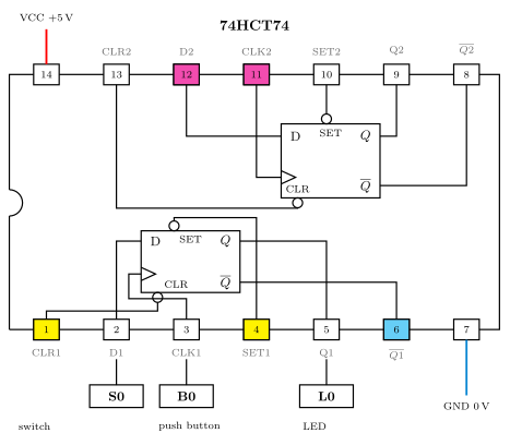
Figure 2: The wired-up 74HCT74: the 14-pin package with both flip-flops inside, the three highlighted pin groups, and the only three external connections the circuit actually makes. The fill colours mark the three cases, one colour each - magenta for pins 11 and 12, yellow for pins 1 and 4, cyan for pin 6 - and mean nothing beyond that grouping; red and blue mark the supply stubs. The three connections are switch S0 to D1 (pin 2), push button B0 to CLK1 (pin 3) and LED L0 to Q1 (pin 5). The signal names outside each pin box are from the device sheet’s pin table (device-pinouts).
Reading the figure: the circuit uses only the first flip-flop. The second one (pins 8–13) is wired to nothing at all, and of the first flip-flop’s six pins only three are driven or read.
| Disconnected | Matters? |
|---|---|
Pins 11 and 12 — CLK2 and D2, the clock and data of the second, entirely unused flip-flop |
No. That half’s outputs (pins 8 and 9) go nowhere, so whatever its flip-flop does is invisible. Untidy rather than wrong; good practice is to tie unused inputs to a fixed level so the chip isn’t switching at random and drawing current. |
| Pin 6 — \(\overline{Q1}\), the complement output of the flip-flop you are using | No. It is an output. Leaving an output unconnected is always safe; it is only ever a problem to leave an input undriven. |
Pins 1 and 4 — CLR1 and SET1 of the flip-flop you are using |
Yes, badly. These are active-low asynchronous inputs. Floating, they can assert at random and clear or set the flip-flop behind your back, so \(Q\) changes with no clock edge in sight. They must be tied high. |
The distinction to take away: a floating input on a device you are using is a real fault; a floating output is harmless; a floating input on a section you are not using is merely untidy.
A naming clash worth knowing about. The device sheet calls pins 4 and 1
SETandCLR; Task 3 below calls the same two pinsPREandCLR; flip-flops-and-latches writes them \(\overline{\text{PRE}}\) and \(\overline{\text{CLR}}\). The course is inconsistent about this (see csse2010-diagram-notation). The pinout figure uses the device sheet’s names, and the Task 3 section below usesPRE/CLRfor the two push buttons while the chip symbol inside its schematic keeps the device sheet’sSET/CLRon pins 4 and 1. Same two pins, two names, one figure.
The same trap comes back in Lab 4 as the 74HCT157’s active-low ENABLE, which must be tied low for the chip to work at all — see week3-lab-lab-4-pre-work — and again in Lab 7, see week4-lab-lab-7-exercises.
Tasks 1 and 2 — simulate the S-R latches
- Simulate the active-high S-R latch (cross-coupled NOR gates) in Logisim and verify its operation.
- Simulate the active-low S-R latch (cross-coupled NAND gates) and verify its operation.
Both circuits, both truth tables, and why the NAND version’s set/reset roles invert and its inputs are drawn overlined, are in flip-flops-and-latches.
The thing to actually verify in the simulator is the part a truth table hides: the hold row, where both inputs are inactive and the latch keeps whatever it had. Drive it into set, return the inputs to their inactive values, and check the output stays put — that is the memory, and it is the only behaviour that distinguishes a latch from a gate.
Task 3 — build a 74HCT74 circuit
The circuit to implement is a 2-input AND gate fed by \(A\) and \(B\), whose output drives the \(D\) input of a rising-edge-triggered D flip-flop.
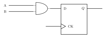
Figure 3: The Task 3 circuit - two switch inputs ANDed into D, one clock input on a wedge (so edge-triggered), Q out. The clock is labelled CK, which is one of the four spellings this course uses for that pin. Nothing else is drawn: the asynchronous inputs and Q-bar are left off, even though the task requires both to be wired.
So \(Q\) takes the value of \(A \cdot B\) on each rising clock edge and holds it until the next one. Drawing the schematic means adding what this logic diagram leaves out. The task asks for a schematic that:
- uses a
74HCT74(and other chips as needed) — the AND gate needs a second chip; - uses push buttons for the CLK (CK), PRE and CLR inputs;
- uses switches for the A and B inputs;
- uses LEDs for the \(Q\) and \(\overline{Q}\) outputs.
Have it checked by a tutor, then build and test it.
Why put inverters between the buttons and the PRE/CLR inputs?
Because \(\overline{\text{PRE}}\) and \(\overline{\text{CLR}}\) are active low, and a push button is the wrong shape for an active-low input. What the flip-flop needs is a pin that sits reliably high whenever you are not asking for a preset or clear, and goes low only while you press — otherwise the asynchronous input is asserted at rest and the clocked behaviour you are trying to test never happens. Putting an inverter between the button and the pin turns the button’s natural “pressed = high” into the “pressed = low” the pin wants, and holds the pin high the rest of the time. (Asserting \(\overline{\text{PRE}}\) and \(\overline{\text{CLR}}\) at once is an illegal input; see flip-flops-and-latches.)
This is the same problem as the floating-pin question above. Pins 1 and 4 must be held high and only pulsed low, and neither leaving them floating nor wiring a bare button to them achieves that.
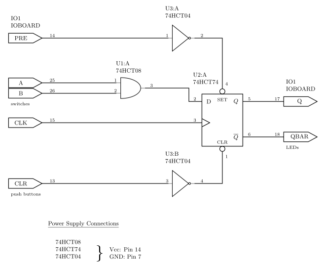
Figure 4: The Task 3 schematic. Three chips: U1 for the AND gate, U2 for the flip-flop, U3 for the two inverters that make the active-low PRE and CLR usable from push buttons. All three are 14-pin parts sharing Vcc 14 and GND 7, so one power block covers them. The pin assignments and the IO board pin numbers are from device-pinouts.
Test it the way Lab 4 asks you to test everything (see week3-lab-lab-4-pre-work): decide the expected behaviour first. Here that is four rows of \(A \cdot B\) crossed with “did a clock edge happen”, plus two asynchronous checks — press PRE with \(A\cdot B = 0\) and confirm \(Q\) goes high without a clock edge, then press CLR and confirm it goes low the same way.
Kit borrowing
- Fill in, sign and submit the kit borrowing agreement (also on Blackboard), then collect your kit. Wait at your table; don’t queue.
- Check all the parts are there and write your student number on the kit.
- Don’t use the kit until advised — some parts break easily, especially the USB connector on the I/O board (see io-board).
- You’ll start with the logic chips and breadboard, and will be advised how to use them. The AVR microcontroller is only needed in the second half of the course — leave those parts alone until then.
- Drop the course after borrowing? Return the kit within 3 business days to the EECS school office, building 78 room 425. (If you’re thinking of dropping, don’t borrow one.)
- The kit must be returned by the end of semester in working order.
Dongles
By the end of semester you’ll be using two USB-A cables for data — one for programming, one for serial communication — and one of them from about halfway through. On your own laptop you may need a dongle. There are workarounds but they all have downsides, so get one sooner rather than later.
Next
Lab 6 has a preparation task — the combination lock, spelled out in 2026-08-13-shift-registers — to be done before the session. See week4-lab-sequential-circuits-shift-registers.