Sequential Circuits 1 — Shift Registers
Learning Lab 6 — the four-mode shift-register design exercise, then the combination lock from the preparation task. Pairs with 2026-08-13-shift-registers, which carries the full preparation-task spec, and with shift-registers for the mux-per-flip-flop construction the exercise turns on.
Lab plan
- Sequential circuits — the shift register exercise
- The combination lock preparation task — discuss with staff and others at your table
- The combination-lock example is set up at the end of Week 3, Lecture 6 (see the lecture note); read it first
- Modifying the combination lock
- Make sure you can draw a circuit schematic and simulate in Logisim. If in doubt, ask.
Ed Lessons — C is starting
The Ed discussion board also hosts Ed Lessons, teaching the basics of C. The content is no more complex than CSSE1001, and C programming for the AVR starts in week eight. Staggered release:
| Date | Release |
|---|---|
| 14 Aug | Basics (out now) |
| 28 Aug | Next Steps #1 |
| 11 Sep | Next Steps #2 |
| 25 Sep | Extension Tasks |
| 16 Oct | Floating Point Workshop |
Exercise — the four-mode shift register
The exercise is a half-drawn circuit to finish. What is already wired matters as much as what is missing.
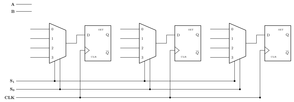
Figure 1: The half-drawn circuit to complete. Three stages, not four: each is a 4-to-1 multiplexer (trapezoid, wide edge left, data inputs numbered 0-3 top to bottom, select inputs entering the bottom sloping edge) feeding one edge-triggered D flip-flop. Already wired for you are the mux outputs into the D inputs and the three shared rails - S1 and S0 into every mux’s select, CLK into every flip-flop. Left bare are the twelve mux data inputs and the A and B stubs at the top left: filling those in is the whole exercise. Junction dots mark connections; lines that cross without a dot are not connected.
Complete the design so that it implements this behaviour:
| \(S_1 S_0\) | Action when the circuit is clocked |
|---|---|
00 |
Bits shifted to the right; the value on \(A\) is stored in the leftmost flip-flop |
01 |
All bit values are toggled |
10 |
If \(B\) is 1, the value from \(A\) is stored in all flip-flops; if \(B\) is 0, all flip-flops reset (i.e. 0 is stored in all flip-flops) |
11 |
All bits are rotated to the left. (Bit in leftmost flip-flop is moved to rightmost flip-flop) |
Hint: construct the truth table for \(f(A,B)\).
What the hint is for
Three of the four modes pick a source for each \(D\) input — some other flip-flop’s output, or that flip-flop’s own complement. Mode 10 is the only one that has to compute something from the primary inputs, and the hint says to nail it down as a truth table before wiring anything:
| \(A\) | \(B\) | What the row asks for | \(f\) |
|---|---|---|---|
| 0 | 0 | \(B=0\), so reset — store 0 | 0 |
| 0 | 1 | \(B=1\), so store \(A\) — store 0 | 0 |
| 1 | 0 | \(B=0\), so reset — store 0 | 0 |
| 1 | 1 | \(B=1\), so store \(A\) — store 1 | 1 |
\[\boxed{f(A,B) = A \cdot B}\]
One AND gate, its output fanned out to input 2 of all three multiplexers. “Load \(A\)” and “reset” are not two behaviours needing two circuits — they are the same wire, because \(B\) gates \(A\) to zero.
Where each mux input comes from
Name the flip-flops \(Q_2 Q_1 Q_0\), leftmost first, matching the bit ordering used in shift-registers. Input \(n\) of every mux is the one selected by \(S_1S_0 = n\), so the mode table becomes a wiring table:
| Mux input | Mode | Leftmost (\(D_2\)) | Middle (\(D_1\)) | Rightmost (\(D_0\)) |
|---|---|---|---|---|
| 0 | 00 shift right |
\(A\) | \(Q_2\) | \(Q_1\) |
| 1 | 01 toggle |
\(\overline{Q_2}\) | \(\overline{Q_1}\) | \(\overline{Q_0}\) |
| 2 | 10 load / reset |
\(f = A\cdot B\) | \(f\) | \(f\) |
| 3 | 11 rotate left |
\(Q_1\) | \(Q_0\) | \(Q_2\) |
Three things fall out of that table, and they are what the exercise is really testing:
- The toggle mode needs no gates at all. Every D flip-flop already publishes \(\overline{Q}\), so input 1 of each mux is a wire back from the stage’s own complementary output. Feeding \(\overline{Q}\) into \(D\) is the standard way to make a flip-flop toggle — it is the same \(D = \overline{Q}\) wiring counters gives for a 1-bit counter.
- The load/reset mode needs exactly one gate, shared, because \(f\) does not depend on the stage.
- Rotate left is shift right’s column read backwards, plus a wrap. Input 0 always comes from the neighbour on the left, input 3 always from the neighbour on the right; the only asymmetry is at the ends — the leftmost stage takes \(A\) for input 0 (there is no neighbour, and the bit shifted out of \(Q_0\) is simply lost), and the rightmost stage takes \(Q_2\) for input 3.
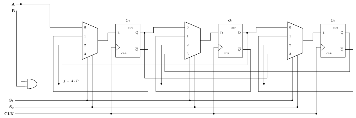
Figure 2: The completed design. Each mux input takes the source its select code names: 0 shifts right (from the left-hand neighbour’s Q, or from A at the left end), 1 toggles (the stage’s own Qbar, which the flip-flop already provides, so no inverter is needed anywhere), 2 loads f = A.B (one AND gate shared by all three stages), 3 rotates left (from the right-hand neighbour’s Q, with Q2 wrapping round to the rightmost stage). The flip-flops are named Q2 Q1 Q0 left to right, matching the bit ordering used in shift-registers. Lines crossing without a junction dot are not connected - that rule is doing a lot of work in the band of return wires below the row.
A trace
A check of the wiring above. Start at \(Q_2Q_1Q_0 = 101\) and hold \(A = 1\), \(B = 1\) except where noted:
| \(S_1S_0\) | Mode | Before | After |
|---|---|---|---|
00 |
shift right, \(A=1\) in at the left | 101 | 110 |
01 |
toggle | 110 | 001 |
11 |
rotate left | 001 | 010 |
10 |
\(B=1\): load \(A=1\) everywhere | 010 | 111 |
10 |
\(B=0\): reset | 111 | 000 |
The rotate row is the one worth checking twice: \(Q_2 \leftarrow Q_1 = 0\), \(Q_1 \leftarrow Q_0 = 1\), and the bit that was in the leftmost flip-flop, \(Q_2 = 0\), wraps into the rightmost.
Discussing your diagrams
The lab runs a schematic review. The checklist:
Logic diagram — circuit functionality: will it do what was asked?
Circuit schematic —
- naming of inputs and outputs
- identification of chips (
U1,U2, …) and gates within chips where applicable (:A,:B, …) - identification of types of chips (
74HCT00etc.) - numbering of pins
- power supply connections
Check the schematic guide and device pinouts on Blackboard for more detail, and ask a staff member if necessary. Full rules in circuit-schematics; pinouts in device-pinouts.
Combination lock tasks
The preparation task itself — a two-stage 4-bit shift register, four switches, clock and reset buttons, locked/unlocked LEDs, and a code derived from your student number — is spelled out in 2026-08-13-shift-registers, which also carries the block diagram and the ordering trap (you enter the left code digit first, so it is the older one and ends up in the second stage).
Task 1 — test your combination lock design.
Task 2 — use fewer flip-flops. On paper, design something that detects the sequence AC in hex: switches set to A (1010), clock push-button pressed; switches set to C (1100), clock push-button pressed.
Can you do it with 3 flip-flops? Can you do it with 2? (Hint: can you move the registers towards the output side?)
Working — Task 2
The basic lock stores both digits and compares afterwards: two 4-bit stages, eight flip-flops, feeding a combinational code check. But the digits themselves are never needed downstream — only whether each was the expected one. So compare first, and register the verdict:
\[P = W_3\overline{W_2}W_1\overline{W_0} \quad (\text{switches show A} = 1010_2) \qquad C = W_3W_2\overline{W_1}\,\overline{W_0} \quad (\text{switches show C} = 1100_2)\]
- Flip-flop 1: \(D_1 = P\). After a clock, \(Q_1 = 1\) means the digit just entered was A.
- Flip-flop 0: \(D_0 = Q_1 \cdot C\). After the next clock, \(Q_0 = 1\) means the last two digits entered were A then C.
- unlocked LED \(= Q_0\); locked LED \(= \overline{Q_0}\), taken straight off the flip-flop.
Two flip-flops, down from eight. The combinational cost barely moves — the original design also has to compare two 4-bit values against the code, so \(P\) and \(C\) are the same two equality checks moved to the other side of the flip-flops, plus one AND. The whole saving is in storage.
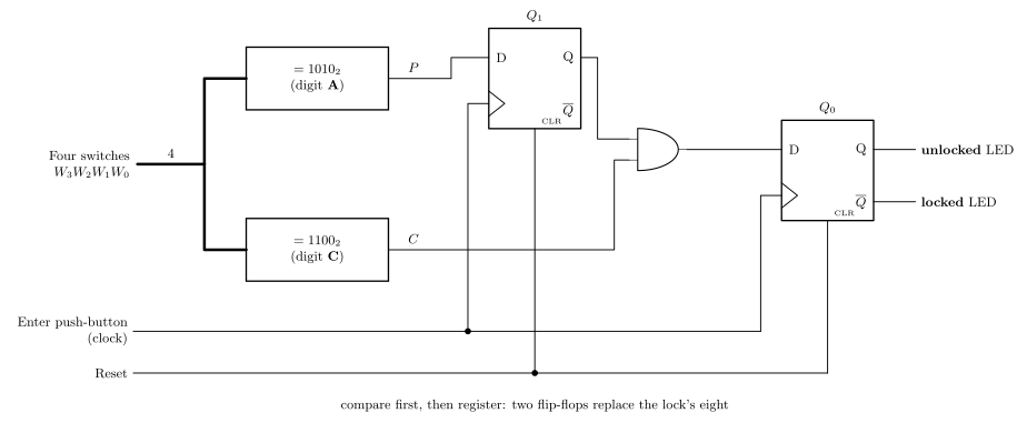
Figure 3: Task 2’s two-flip-flop AC detector. This is the hint ‘move the registers towards the output side’ drawn out: the four switches are compared against the two expected digits combinationally, and only the one-bit verdicts are clocked, so the eight flip-flops of the basic lock (compare after storing, see the block diagram in 2026-08-13-shift-registers) collapse to two. Q1 remembers ‘the digit just entered was A’; Q0 is the unlock verdict, and it is a registered output, so the LEDs change only when the enter button is pressed. The locked LED needs no inverter - the flip-flop’s Qbar is already the complement. Lines crossing without a junction dot are not connected. The comparators are drawn as plain blocks, and the four-switch bus is drawn heavy with its width lettered beside it, which is neither of the two ways the course marks bus width (a slash across the line with the width beside it, or the width lettered next to a plain line).
Why not one? With a single flip-flop holding “the last digit was A” and the LED driven combinationally by \(Q_1 \cdot C\), the lock would open the instant the switches were set to C — before the enter button was pressed. That is a Mealy output, and it is not what the original lock does. Registering the verdict is what keeps the LEDs changing only on a clock edge. Two is also the floor for a Moore machine here: the circuit must distinguish three situations — nothing useful yet, A just entered, AC just entered — and three states need two flip-flops. See state-machines.
Three flip-flops. Reading the question as a ladder, three flip-flops is what a one-hot encoding of those same three states costs — one flip-flop per state — and going to a binary encoding is what buys the drop to two. The compare-then-register construction lands on two directly, so three is a waypoint rather than a separate design.
Simulate and test.
Task 3 — challenge. Allow the unlock combination itself to be set and stored in flip-flops using switches and buttons, rather than hard-wired. Simulate and test.
The expected trajectory: for each of tasks 1 and 2, logic/schematic diagrams completed → partially working circuit → fully working circuit, with task 3 only at the diagram stage.
Next
Lab 7 has a preparation task, and it is to be done before you arrive for the practical session — see week4-lab-lab-7-exercises.
See also
- shift-registers · combinational-logic-blocks — the 4-to-1 mux and the mux-per-flip-flop stage
- 2026-08-13-shift-registers — Lecture 6, and the full preparation-task specification
- circuit-schematics · device-pinouts — the schematic-review checklist above, in full
- csse2010-diagram-notation — the mux and flip-flop symbol conventions these figures follow