Lab 7 Exercises
exercises
lab
computer-systems
digital-logic
sequential-logic
NoteProvided task
Pre-Lab Preparation
You should complete a circuit schematic diagram as described below before your Lab 7 session in week 4 (Thu-Fri). You should consult the device pinout information on Blackboard (captured in device-pinouts; the drawing rules it has to satisfy are in circuit-schematics). You will be testing this circuit (or a similar circuit) during the prac session.
Design Requirements
Design and draw a circuit schematic diagram for a 3-bit synchronous counter which counts through your allocated sequence (see table below).
Hardware Specifications:
- Clock: You must use a push button for the clock signal.
- Preset: Use a single switch to allow your counter to be preset (i.e., to
111). - Clear: Use a single switch to allow your counter to be cleared (i.e., to
000). - Outputs: Your count output should be shown on three LEDs.
- \(Q_2\): Most Significant Bit (MSB)
- \(Q_1\): Middle bit
- \(Q_0\): Least Significant Bit (LSB)
Note: Your allocated sequence has seven binary numbers; you may choose to do whatever you like with the missing number – i.e., if the counter ever has this value, then we treat the next count value as a “don’t care” condition.
It is highly recommended that you simulate your circuit using Logisim to ensure it counts through the expected sequence.
Count Sequences
Find the sequence corresponding to the last digit of your 8-digit UQ student number:
| Last digit of UQ ID | Count Sequence |
|---|---|
| 0 | 111 -> 011 -> 101 -> 110 -> 001 -> 000 -> 010 -> 111 -> … |
| 1 | 111 -> 010 -> 101 -> 110 -> 100 -> 000 -> 001 -> 111 -> … |
| 2 | 000 -> 011 -> 010 -> 110 -> 100 -> 001 -> 111 -> 000 -> … |
| 3 | 111 -> 100 -> 101 -> 000 -> 110 -> 001 -> 011 -> 111 -> … |
| 4 | 000 -> 101 -> 011 -> 010 -> 001 -> 110 -> 100 -> 000 -> … |
| 5 | 000 -> 110 -> 001 -> 100 -> 111 -> 011 -> 010 -> 000 -> … |
| 6 | 111 -> 010 -> 000 -> 110 -> 001 -> 101 -> 100 -> 111 -> … |
| 7 | 111 -> 001 -> 110 -> 101 -> 100 -> 000 -> 010 -> 111 -> … |
| 8 | 111 -> 000 -> 001 -> 101 -> 011 -> 110 -> 100 -> 111 -> … |
| 9 | 000 -> 100 -> 001 -> 110 -> 101 -> 011 -> 010 -> 000 -> … |
Working
My student number is ——6, so I will be sequencing: 111 -> 010 -> 000 -> 110 -> 001 -> 101 -> 100 -> 111 -> …
Let’s map the current and next states:
| Current State (\(Q_2 Q_1 Q_0\)) | Next State (\(D_2 D_1 D_0\)) | Comment |
|---|---|---|
0 0 0 |
1 1 0 |
\(000 \to 110\) |
0 0 1 |
1 0 1 |
\(001 \to 101\) |
0 1 0 |
0 0 0 |
\(010 \to 000\) |
0 1 1 |
X X X |
unused state |
1 0 0 |
1 1 1 |
\(100 \to 111\) |
1 0 1 |
1 0 0 |
\(101 \to 100\) |
1 1 0 |
0 0 1 |
\(110 \to 001\) |
1 1 1 |
0 1 0 |
\(111 \to 010\) |
Deriving \(D_2\)
Rows where \(D_2 = 1\):
| \(Q_2 Q_1 Q_0\) | \(D_2\) |
|---|---|
0 0 0 |
1 |
0 0 1 |
1 |
1 0 0 |
1 |
1 0 1 |
1 |
Each row gives one product term (1 for that row, 0 elsewhere):
\[ \begin{aligned} D_2 &= \bar{Q_2} \cdot \bar{Q_1} \cdot \bar{Q_0} + \bar{Q_2} \cdot \bar{Q_1} \cdot Q_0 + Q_2 \cdot \bar{Q_1} \cdot \bar{Q_0} + Q_2 \cdot \bar{Q_1} \cdot Q_0 \\ &= \bar{Q_2} \cdot \bar{Q_1} \left(\bar{Q_0} + Q_0\right) + Q_2 \cdot \bar{Q_1} \left(\bar{Q_0} + Q_0\right) & \text{(Distributive law)} \\ &= \bar{Q_2} \cdot \bar{Q_1} \cdot \mathbf{t} + Q_2 \cdot \bar{Q_1} \cdot \mathbf{t} & \text{(Negation law)} \\ &= \bar{Q_2} \cdot \bar{Q_1} + Q_2 \cdot \bar{Q_1} & \text{(Identity law)} \\ &= \bar{Q_1} \left(\bar{Q_2} + Q_2\right) & \text{(Distributive law)} \\ &= \bar{Q_1} \cdot \mathbf{t} & \text{(Negation law)} \\ &= \bar{Q_1} & \text{(Identity law)} \end{aligned} \tag{1}\]
\(D_2\) is just \(\bar{Q_1}\), so it needs no gate at all. FF1’s \(\overline{Q}\) output wires straight to FF2’s \(D\) input.
Deriving \(D_1\)
Sum of products where \(D_1 = 1\) (000, 100, 111):
\[ \begin{aligned} D_1 &= \bar{Q_2} \cdot \bar{Q_1} \cdot \bar{Q_0} + Q_2 \cdot \bar{Q_1} \cdot \bar{Q_0} + Q_2 \cdot Q_1 \cdot Q_0 & \\ &= \bar{Q_1} \cdot \bar{Q_0} \left(\bar{Q_2} + Q_2\right) + Q_2 \cdot Q_1 \cdot Q_0 & \text{(Distributive law)} \\ &= \bar{Q_1} \cdot \bar{Q_0} \cdot \mathbf{t} + Q_2 \cdot Q_1 \cdot Q_0 & \text{(Negation law)} \\ &= \bar{Q_1} \cdot \bar{Q_0} + Q_2 \cdot Q_1 \cdot Q_0 & \text{(Identity law)} \end{aligned} \tag{2}\]
Deriving \(D_0\)
Sum of products where \(D_0 = 1\) (001, 100, 110), plus the unused state 011 — its next state is a don’t care, so I am free to take \(D_0 = 1\) there, which lets \(Q_1\) cancel:
\[ \begin{aligned} D_0 &= \bar{Q_2} \cdot \bar{Q_1} \cdot Q_0 + \bar{Q_2} \cdot Q_1 \cdot Q_0 + Q_2 \cdot \bar{Q_1} \cdot \bar{Q_0} + Q_2 \cdot Q_1 \cdot \bar{Q_0} & \\ &= \bar{Q_2} \cdot Q_0 \left(\bar{Q_1} + Q_1\right) + Q_2 \cdot \bar{Q_0} \left(\bar{Q_1} + Q_1\right) & \text{(Distributive law)} \\ &= \bar{Q_2} \cdot Q_0 \cdot \mathbf{t} + Q_2 \cdot \bar{Q_0} \cdot \mathbf{t} & \text{(Negation law)} \\ &= \bar{Q_2} \cdot Q_0 + Q_2 \cdot \bar{Q_0} & \text{(Identity law)} \\ &= Q_2 \oplus Q_0 & \text{(definition of XOR)} \end{aligned} \tag{3}\]
\(\bar{Q_2} \cdot Q_0 + Q_2 \cdot \bar{Q_0}\) is exclusive-or, so \(D_0\) is a single XOR gate.
Checking Robustness
011 was left unused in Table 2, so its next state was treated as a don’t care when deriving Equation 1, Equation 2 and Equation 3. The circuit will still compute something for this state, so I need to check it doesn’t get stuck there. Substituting \(Q_2 Q_1 Q_0 = 011\) into each equation:
\[ \begin{aligned} D_2 &= \bar{Q_1} \\ &= \bar{1} \\ &= 0 \end{aligned} \tag{4}\]
\[ \begin{aligned} D_1 &= \bar{Q_1} \cdot \bar{Q_0} + Q_2 \cdot Q_1 \cdot Q_0 \\ &= \bar{1} \cdot \bar{1} + 0 \cdot 1 \cdot 1 \\ &= 0 \cdot 0 + 0 \\ &= 0 \end{aligned} \tag{5}\]
\[ \begin{aligned} D_0 &= Q_2 \oplus Q_0 \\ &= 0 \oplus 1 \\ &= 1 \end{aligned} \tag{6}\]
So \(D_2 D_1 D_0 = 001\), meaning 011 -> 001. This is not 011 itself, and 001 is already part of my sequence, so the counter does not lock up in the unused state: it self-corrects back into the main count sequence within one clock cycle.
Taking the don’t care as a 1 in \(D_1\) as well would have simplified it to \(\overline{Q_1 \oplus Q_0}\), but then 011 -> 011 and the counter would hang, so I only used it for \(D_0\).
Conclusion
As per Equation 1, Equation 2 and Equation 3, the excitation equations for the counter are:
\[ \begin{aligned} D_2 &= \bar{Q_1} \\ D_1 &= \bar{Q_1} \cdot \bar{Q_0} + Q_2 \cdot Q_1 \cdot Q_0 \\ D_0 &= Q_2 \oplus Q_0 \end{aligned} \tag{7}\]
and the robustness check in Equation 4, Equation 5 and Equation 6 confirms that the one unused state, 011, transitions to 001 rather than to itself. The counter is therefore self-correcting, and these three equations fully and safely implement my allocated count sequence.
That comes to five 2-input gates across five chips. The breadboard only fits six, so this leaves one spare. No inverters are needed anywhere: the 74HCT74 gives \(\overline{Q}\) alongside \(Q\), so \(\overline{Q_1}\) and \(\overline{Q_0}\) are free.
Circuit Schematic
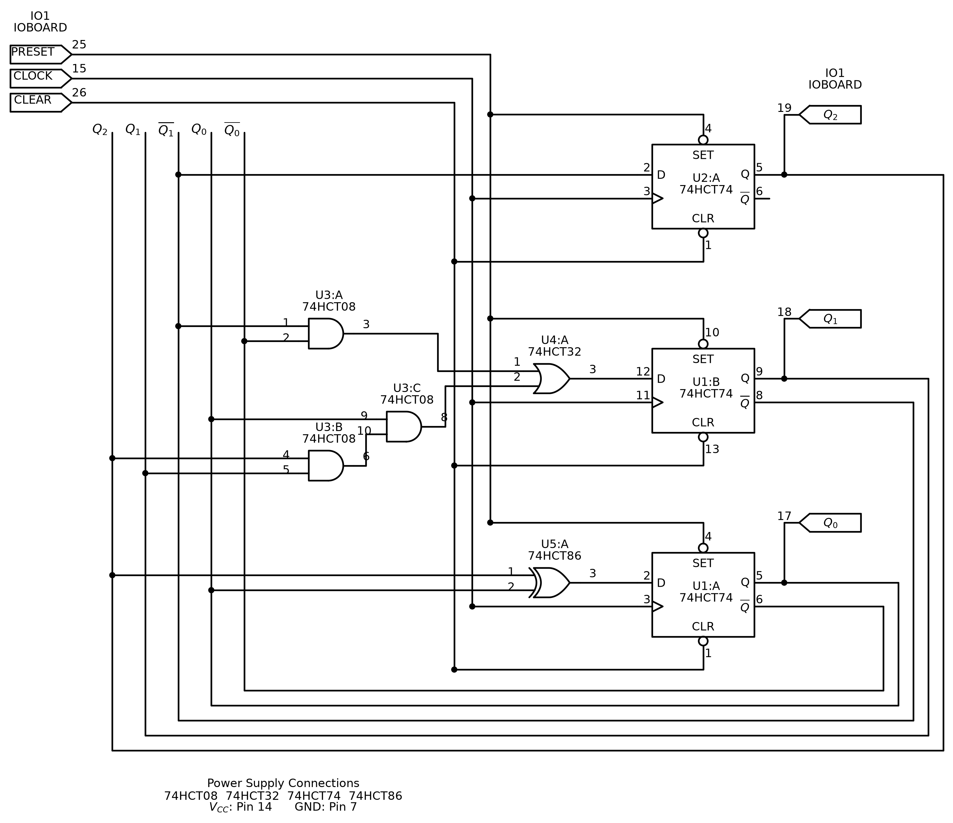
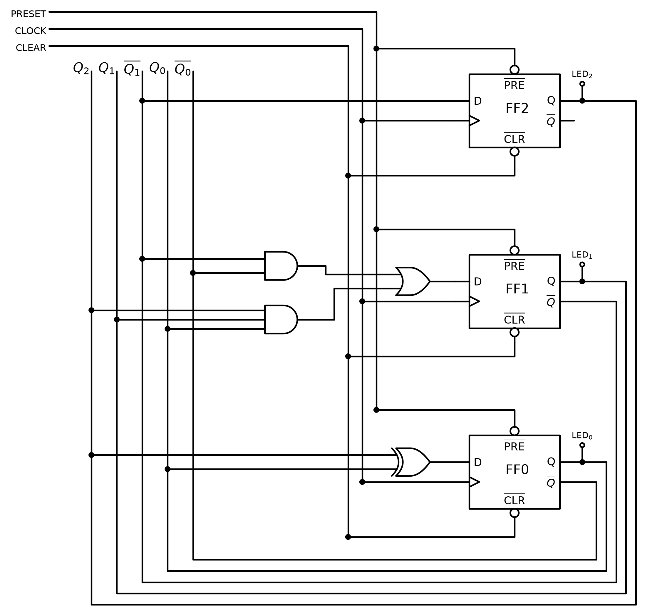
Figure 1 is a logic diagram. Figure 2 is the same counter drawn as a circuit schematic (see circuit-schematics), with device IDs, chip types and pin numbers from device-pinouts.
It takes five chips: U1 and U2 are 74HCT74 dual flip-flops, U3 a 74HCT08 (the 3-input product is U3:B and U3:C cascaded, since the kit has no 3-input gate), U4:A a 74HCT32 and U5:A a 74HCT86. On the IO board, CLOCK is button B0, PRESET and CLEAR are switches S0 and S1, and \(Q_2 Q_1 Q_0\) drive LEDs L2, L1 and L0.