CSSE2010 — Full Course Notes
Week 1
Lecture 1 — Course Introduction; Bits, Bytes and Binary
See csse2010 for staff, assessment, and course logistics — this note covers the technical content from Lecture 1.
Today’s outline
- Course intro, organisation and admin
- Assessment details
- Technical content — binary numbers
Levels of abstraction
A computer can be understood at several levels of increasing abstraction (from Tanenbaum’s Structured Computer Organisation):
- Level 0 — Digital Logic level (gates, circuits) — this course starts here
- Level 1 — Microarchitecture level
- Level 2 — Instruction set architecture level
- Level 3 — Operating system machine level
- Level 4 — Assembly language level
- Level 5 — Problem-oriented language level
The course roughly climbs this stack over the semester: hardware/digital logic first, then low-level (assembly) software, then high-level software.
Computers and binary numbers
Computers represent everything — inputs, instructions, and outputs — as binary data internally, e.g. 101001010110101001111010101001011100011010101.
See binary-number-representations for the full reference on bits, bytes, unsigned number representation, converting between decimal/binary/octal/hex, and radix notation conventions — all introduced in this lecture.
Reminders
- Sign up to a pair of lab sessions (P2, P1).
- Labs start from Thursday of week 1 (P1 sessions only — no P2 sessions in week 1).
- From week 2, both P2 and P1 sessions run.
- Lab 1 covers different binary representation formats for signed numbers (two’s complement etc. — not covered in this lecture).
- A summary recording on binary numbers will be posted by the end of week 1.
- Lab sign-on issues: email eait.mytimetable@uq.edu.au.
Lecture 2 — Intro to Logic Gates
See logic-gates and boolean-algebra for the reference definitions/tables this lecture introduces.
Today’s outline
- Introduction to Logic Gates
- Logic Diagrams
- Boolean Algebra and Logic Expressions
Digital logic
- Digital circuits only have two logical levels present (binary): logic ‘0’ (~0V) and logic ‘1’ (~0.8-5V, depending on the logic family/transistor type).
- Logic gates are the building blocks of computers: each has one or more inputs and exactly one output, and performs a logic operation.
- 7 basic gate types: NOT, AND, OR, NAND, NOR, XOR, XNOR — see logic-gates for symbols and truth tables.
- Every logic function can be described four equivalent ways: logic symbol, truth table, Boolean expression, timing diagram.
Quiz: 3-input NAND truth table
Given four candidate truth tables, which one is the 3-input NAND?
Reasoned from the definition (NAND = NOT(AND), and AND is 1 only when all inputs are 1): the correct table is the one where \(X = 1\) for every combination except \(A=B=C=1\) (where \(X=0\)).
Quiz: 3-input XOR truth table
XOR is the “odd function” — \(X=1\) exactly when an odd number of inputs are 1.
Reasoned from that definition, the correct table (in order \(ABC = 000, 001, 010, 011, 100, 101, 110, 111\)) is: \[X = 0, 1, 1, 0, 1, 0, 0, 1\]
Boolean algebra conventions
See boolean-algebra for the full notation conventions, laws/identities table, and De Morgan’s law diagrams introduced in this lecture.
Logic diagram conventions
- A filled dot at a wire junction indicates an electrical connection; wires that cross without a dot are not connected.
- Inputs are conventionally drawn on the left, outputs on the right.
Gates on ICs
- Example: the 74HCT00 IC has four 2-input NAND gates in a single 14-pin DIP package.
- Vcc = power (e.g. 5V), GND = ground (0V). Pin spacing 0.1”×0.3”; chip ~15mm long.
Logic function implementation (sum of products)
Any logic function can be implemented as the OR of AND combinations of its inputs — called sum of products: for each row where the output is 1, write the AND of the inputs (complemented where 0) that produces that row, then OR all those terms together.
Worked example — truth table for \(M\):
| A | B | C | M |
|---|---|---|---|
| 0 | 0 | 0 | 0 |
| 0 | 0 | 1 | 0 |
| 0 | 1 | 0 | 0 |
| 0 | 1 | 1 | 1 |
| 1 | 0 | 0 | 0 |
| 1 | 0 | 1 | 1 |
| 1 | 1 | 0 | 1 |
| 1 | 1 | 1 | 1 |
\[M = \bar A BC + A\bar B C + AB\bar C + ABC\]
Equivalent functions (simplification)
Sum-of-products doesn’t necessarily give the minimum number of gates — Boolean algebra laws (see boolean-algebra) can be used to manipulate an expression into an equivalent, simpler one.
Example: \(Z = AB + AC = A(B+C)\) (distributive law) — the right-hand form needs fewer gates.
Universal (complete) gates
All circuits can be built from NAND-only or NOR-only gates (called complete/universal gates) — NOT, AND, and OR can each be constructed purely from NAND gates (or purely from NOR gates). This matters in practice because NAND and NOR gates are easier to build from transistors than AND/OR directly.
Reminders
- Attend Learning Lab sessions for the second half of this week — only the session you’re signed up to.
- From week 2, you’ll have both P2 (Mon-Tue) and P1 (Thu-Fri) lab sessions.
Week 1 Exercises — Bits, Bytes & Binary; Intro to Logic Gates
Practice exercises for week 1, covering 2026-07-27-course-intro-bits-bytes-binary and 2026-07-30-intro-to-logic-gates. Many are taken from or based on Tanenbaum, Structured Computer Organisation, 5th edition, Appendix A and Appendix B. See binary-number-representations and logic-gates for the reference material needed to solve these.
On the HTML site, fill in each blank with your answer (as a quoted string, e.g. "1010"), then click Run Code to check it. In the PDF, the Working callout is shown as a static answer key instead (interactive checking needs a browser).
Q1 — Decimal to binary conversion
Convert the following decimal numbers to binary (unsigned representation): 1984, 4000, 8192.
1984 →
4000 →
8192 →
NoteWorking
Repeatedly divide by 2, reading the remainders bottom-to-top (or subtract the largest power of 2 not exceeding the remaining value) — see binary-number-representations#converting-decimal-to-binary.
- \(1984 = 1024+512+256+128+64 = 2^{10}+2^9+2^8+2^7+2^6 \Rightarrow\)
11111000000 - \(4000 = 2048+1024+512+256+128+32 = 2^{11}+2^{10}+2^9+2^8+2^7+2^5 \Rightarrow\)
111110100000 - \(8192 = 2^{13} \Rightarrow\)
10000000000000(a 1 followed by 13 zeros)
Q2 — Binary to decimal, octal, hexadecimal
What is \(1001101001\) (binary, unsigned) in decimal? In octal? In hexadecimal?
Decimal →
Octal →
Hexadecimal →
NoteWorking
Sum the powers of 2 where a bit is set: \(1001101001_2 = 2^9+2^6+2^5+2^3+2^0 = 512+64+32+8+1 = 617_{10}\).
- Octal: \(617 \div 8 = 77\) r\(1\); \(77 \div 8 = 9\) r\(5\); \(9 \div 8 = 1\) r\(1\); \(1 \div 8 = 0\) r\(1\) →
1151(check: \(1\cdot512+1\cdot64+5\cdot8+1\cdot1=617\)). - Hex: \(617 \div 16 = 38\) r\(9\); \(38 \div 16 = 2\) r\(6\); \(2 \div 16 = 0\) r\(2\) →
269(check: \(2\cdot256+6\cdot16+9=617\)).
Q3 — Counting \(k\)-digit radix-\(r\) numbers
How many different positive integers can be expressed in \(k\) digits using radix \(r\) numbers?
NoteWorking
With \(k\) digits in radix \(r\), every combination from all-zeros to all-\((r-1)\)s is representable, giving \(r^k\) distinct values total (including 0). Excluding 0 leaves \(r^k - 1\) positive integers.
Q4 — Radix-32 (Manchester Mark 1)
One of the earliest computers (the Manchester Mark 1, 1949) was programmed with a radix-32 number system, with digits \(0, 1, \dots 9, A, B, \dots U, V\) (10 numerals + 22 letters = 32 symbols).
- Describe how a binary number can be converted into a radix-32 number.
- Describe how a decimal number can be converted into a radix-32 number.
- Convert the decimal numbers 1300 and 2300 to radix-32 representations.
1300 →
2300 →
NoteWorking
- (a) Binary → radix-32: since \(32=2^5\), group the binary digits into 5-bit groups starting from the least significant bit (pad the leftmost group with leading zeros if needed), then convert each 5-bit group (a value 0–31) to the corresponding single radix-32 digit (0–9, then A=10 … V=31).
- (b) Decimal → radix-32: repeatedly divide by 32, recording each remainder (converting remainders 10–31 to A–V); the radix-32 digits are the remainders read in reverse (last remainder computed = most significant digit) — the same repeated-division method used for decimal → binary/octal/hex.
- (c):
- \(1300 \div 32 = 40\) r\(20\); \(40 \div 32 = 1\) r\(8\); \(1 \div 32 = 0\) r\(1\) → digits \(1, 8, 20\)(=K) →
18K. Check: \(1\cdot1024+8\cdot32+20=1300\). - \(2300 \div 32 = 71\) r\(28\); \(71 \div 32 = 2\) r\(7\); \(2 \div 32 = 0\) r\(2\) → digits \(2,7,28\)(=S) →
27S. Check: \(2\cdot1024+7\cdot32+28=2300\).
- \(1300 \div 32 = 40\) r\(20\); \(40 \div 32 = 1\) r\(8\); \(1 \div 32 = 0\) r\(1\) → digits \(1, 8, 20\)(=K) →
Q5 — Largest unsigned integer
What’s the largest unsigned integer that can be represented in:
- 10 bits
- 9 decimal digits
- 8 hexadecimal digits
(a) 10 bits →
(b) 9 decimal digits →
(c) 8 hexadecimal digits →
NoteWorking
The largest value in \(n\) digits of radix \(r\) is \(r^n - 1\) (all digits at their maximum):
- \(2^{10}-1 = 1023\)
- \(10^9-1 = 999{,}999{,}999\)
- \(16^8-1 = 4{,}294{,}967{,}295\) (note: 8 hex digits = 32 bits, so this equals \(2^{32}-1\))
Q6 — Finger counting
What’s the largest number that can be counted to on ten fingers, if each finger can be considered to have two positions? Compare your answer to that in 5(a).
NoteWorking
Ten fingers, each with 2 possible positions, is exactly 10 bits of information: \(2^{10}-1 = 1023\) — identical to 5(a), since “10 things each with 2 states” is a 10-bit binary number.
Q7 — Signed number formats
For each of the following decimal numbers, write down the 8-bit binary representation using signed magnitude, one’s complement, two’s complement, and excess-128 formats:
- \(-1\)
- \(-16\)
- \(-99\)
Answer as four comma-separated 8-bit codes, in the order signed-magnitude,ones-complement,twos-complement,excess-128 (e.g. "10000000,11111111,00000000,10000000" for 0).
(a) −1 →
(b) −16 →
(c) −99 →
NoteWorking
Formats (see binary-number-representations): signed magnitude = sign bit + 7-bit \(|n|\); one’s complement (negative) = invert every bit of \(|n|\)’s 8-bit form; two’s complement (negative) = \(128+n\) as a 7-bit value, prefixed with a 1; excess-128 = \(n+128\) as a plain 8-bit unsigned value.
| \(n\) | Signed magnitude | One’s complement | Two’s complement | Excess-128 |
|---|---|---|---|---|
| −1 | 10000001 |
11111110 |
11111111 |
01111111 |
| −16 | 10010000 |
11101111 |
11110000 |
01110000 |
| −99 | 11100011 |
10011100 |
10011101 |
00011101 |
Q8 — Signed format ranges
What are the smallest and largest integers that can be represented in the following binary representations:
- 16-bit two’s complement
- \(n\)-bit one’s complement
- excess \(2^{m-1}\)
NoteWorking
- (a) 16-bit two’s complement: smallest \(=-2^{15}=-32768\), largest \(=2^{15}-1=32767\).
- (b) \(n\)-bit one’s complement: symmetric about zero (it has two representations of 0), so smallest \(=-(2^{n-1}-1)\), largest \(=2^{n-1}-1\).
- (c) excess \(2^{m-1}\) (\(m\)-bit field, bias \(2^{m-1}\)): stored value ranges \(0\) to \(2^m-1\), actual value = stored \(-\) bias. Smallest (stored \(=0\)): \(-2^{m-1}\). Largest (stored \(=2^m-1\)): \(2^{m-1}-1\) — the same numeric range as \(m\)-bit two’s complement, just a different (biased) encoding of it.
Q9 — Logic gates: NOR and XOR
Draw the logic symbol, write the Boolean function, and write down the truth table for:
- a 4-input NOR gate
- a 3-input XOR gate (i.e. the odd function)
NoteWorking
(a) 4-input NOR — symbol: an OR-gate body (curved input side, pointed output) with 4 input lines and a small bubble on the output denoting inversion. Boolean function (De Morgan’s): \(X = \overline{A+B+C+D} = \bar A \cdot \bar B \cdot \bar C \cdot \bar D\) — \(X=1\) only when every input is 0.
| A | B | C | D | X |
|---|---|---|---|---|
| 0 | 0 | 0 | 0 | 1 |
| all other 15 combinations | 0 |
(b) 3-input XOR (odd function) — symbol: an XOR-gate body (OR-gate shape with an extra curved line just behind the inputs), no bubble. Boolean function: \(X = A \oplus B \oplus C\) — \(X=1\) iff an odd number of inputs are 1.
| A | B | C | X |
|---|---|---|---|
| 0 | 0 | 0 | 0 |
| 0 | 0 | 1 | 1 |
| 0 | 1 | 0 | 1 |
| 0 | 1 | 1 | 0 |
| 1 | 0 | 0 | 1 |
| 1 | 0 | 1 | 0 |
| 1 | 1 | 0 | 0 |
| 1 | 1 | 1 | 1 |
Week 2
Binary Arithmetic
See binary-number-representations for signed-format background (signed magnitude, two’s complement) and logic-gates/boolean-algebra for the gate-level building blocks used below.
Quiz: -32 in 8-bit signed magnitude
Signed magnitude splits the word into a sign bit (MSB, 1 = negative) and a magnitude in the remaining bits: \(32 = 00100000\), so with the sign bit set this is 10100000 (A).
Quiz: -32 in 8-bit two’s complement
Two’s complement of a positive value: invert all bits, then add 1.
\[00100000 \to \text{invert} \to 11011111 \to +1 \to 11100000\]
So -32 in 8-bit two’s complement is 11100000 (D) — different from the signed-magnitude answer above, which is the point: the same bit pattern means different things depending on the declared format.
Universal gates recap
NOT/AND/OR can each be built from NAND-only or NOR-only gates (see logic-gates for the equivalent-circuit diagrams) — this was revision from last lecture before moving into arithmetic.
Binary addition
Single-bit addition (no carry-in):
| Addend | 0 | 0 | 1 | 1 |
|---|---|---|---|---|
| Augend | +0 | +1 | +0 | +1 |
| Sum | 0 | 1 | 1 | 0 |
| Carry | 0 | 0 | 0 | 1 |
- The bit-wise addition procedure is identical regardless of whether the operands are interpreted as unsigned or two’s complement — only the interpretation of the result differs.
- Two’s complement: the carry-out from the MSB is simply discarded to get the correct result.
- One’s complement: the carry-out from the MSB must be added back into the result (end-around carry) — a practical drawback of one’s complement versus two’s complement.
Worked example (8-bit):
  Decimal   Unsigned      Decimal   2's complement
  10        00001010      10        00001010
+ 243     + 11110011    +(-13)    + 11110011
--------- ------------  -------   -------------
  253       11111101      -3        11111101
Overflow
Overflow: the true result doesn’t fit in the available bits, so the answer is wrong.
- Unsigned: overflow ⟺ carry-out from the MSB.
- Two’s complement: overflow ⟺ carry-in to the MSB ≠ carry-out from the MSB, i.e. \(\text{Overflow} = C_{in} \oplus C_{out}\).
- Equivalently for two’s complement: overflow happens when two positives sum to a negative, or two negatives sum to a positive.
Worked example — both cases overflow:
  Decimal   Unsigned      Decimal   2's complement
  15        00001111      125       01111101
+ 243     + 11110011    +   4     + 00000100
--------- ------------  -------   -------------
  258       00000010     129        10000001   (wraps to -127, wrong)
Quiz: adding two 6-bit two’s complement numbers
\(110101 + 001111\) in 6 bits:
  110101
+ 001111
--------
 1000100   → truncate to 6 bits → 000100
Answer: 000100 (A) — the 7th bit is discarded since we’re constrained to 6 bits (no overflow here since \(C_{in} \oplus C_{out} = 0\) into/out of the MSB).
Half-adder
A device that adds 2 bits with no carry-in.
Truth table (inputs A, B; outputs Sum, Carry):
| A | B | Sum | Carry |
|---|---|---|---|
| 0 | 0 | 0 | 0 |
| 0 | 1 | 1 | 0 |
| 1 | 0 | 1 | 0 |
| 1 | 1 | 0 | 1 |
\[S = A \oplus B \qquad C = AB\]
Full adder
A half-adder alone can’t handle a carry-in from a previous stage, so a full adder takes three inputs (A, B, \(C_{in}\)) and produces Sum and \(C_{out}\):
\[S = A \oplus B \oplus C_{in}\] \[C_{out} = AB + C_{in}(A \oplus B)\]
A full adder is built from two half-adders plus an OR gate: the first half-adder combines A and B; its sum output feeds into a second half-adder along with \(C_{in}\); the two half-adders’ carry outputs are OR’d together to form \(C_{out}\).
Ripple-carry adder
Cascading full adders — each stage’s \(C_{out}\) feeding the next stage’s \(C_{in}\) — builds a multi-bit binary adder (e.g. 4 full adders for 4-bit addition: \(A_3B_3 \ldots A_0B_0 \to S_3 \ldots S_0, C_4\)). For plain addition the initial carry-in \(C_0\) is 0. This structure is called a ripple-carry adder, since the carry has to propagate (“ripple”) through every stage before the final sum is valid.
Reminders
- Week 2 labs: P2 sessions (Mon-Tue) run Lab 2 (Logic Gates); P1 sessions (Thu-Fri) run Lab 3 (Binary Arithmetic).
- Complete the week 1 exercises folder and ask if unclear.
- Watch the summary video on Signed Binary Formats.
Lecture 4 — Combinational Logic
See combinational-logic-blocks for the reference definitions/tables of the adder-subtractor, multiplexer and decoder introduced here, and timing-diagrams for the timing-diagram representation and real-gate timing parameters.
Today’s outline
- Admin
- Binary subtractors
- More combinational logic circuits
- Multiplexers
- Decoders
- Timing diagram representations
Recap — binary adder
Picking up from 2026-08-04-binary-arithmetic: full adders can be cascaded to make a multi-bit binary adder. For 4 bits, four full adders take \(A_3B_3 \ldots A_0B_0\) and produce \(S_3 \ldots S_0\) plus \(C_4\), with each stage’s carry-out \(C_{i+1}\) wired to the next stage’s carry-in. For addition the initial carry-in \(C_0\) is 0. This arrangement is a ripple-carry adder.
Binary subtractors
\(A - B\) is implemented as \(A + (-B)\), with \(-B\) the two’s complement of \(B\) (flip the bits, add 1). The two pieces needed on top of a plain adder are a controlled inverter (an XOR gate per bit, with the mode select \(M\) as the second input) and the extra \(+1\), which is supplied via the adder’s carry-in. Full derivation and the adder-subtractor circuit are in combinational-logic-blocks.
Two slides here are posed as questions and left blank on the handout:
- “How can we use a gate to flip a bit — but only sometimes?” (\(Z = \bar B\) when \(M=1\), \(Z = B\) when \(M=0\).) Derived: a 2-input XOR, \(Z = B \oplus M\).
- “What should carry-in be?” on the adder-subtractor slide. Derived: \(C_0 = M\) — the same mode-select line that drives the XOR gates, so subtract mode automatically contributes the \(+1\) that two’s complement needs.
Combinational circuits in general
A combinational circuit is a combination of logic gates with \(n\) inputs and \(m\) outputs; each output is a function of the \(n\) inputs, the output depends on current inputs only, and it can be written as a truth table with \(n\) input columns, \(m\) output columns and \(2^n\) rows. See combinational-logic-blocks.
Multiplexers
\(2^n\) data inputs, 1 output, \(n\) select inputs that steer one data input to the output. The lecture covered the 4-to-1 mux (logic symbol, function table, and the AND-OR sum-of-products implementation with inverted select literals) and the 2-to-1 mux. Tables and circuit descriptions: combinational-logic-blocks. Off-the-shelf part: the 74HCT157 quad 2-input mux, see device-pinouts.
Quiz: 2-to-1 multiplexer truth table
A 2-to-1 multiplexer has data inputs \(D_0\) and \(D_1\), control input \(S_0\), and output \(F\), with function table \(F = D_0\) when \(S_0 = 0\) and \(F = D_1\) when \(S_0 = 1\). Which of three candidate truth tables (columns \(S_0, D_0, D_1, F\)) goes with this circuit?
Reasoning from the function table, row by row in the order \(S_0 D_0 D_1 = 000, 001, 010, 011, 100, 101, 110, 111\):
- The first four rows have \(S_0 = 0\), so \(F\) must copy \(D_0\) and ignore \(D_1\): \(F = 0, 0, 1, 1\).
- The last four rows have \(S_0 = 1\), so \(F\) must copy \(D_1\) and ignore \(D_0\): \(F = 0, 1, 0, 1\).
\[F = 0,\,0,\,1,\,1,\,0,\,1,\,0,\,1\]
That is option 2. Option 1 has \(F\) following \(D_1\) when \(S_0=0\) and \(D_0\) when \(S_0=1\) — the two data inputs swapped. Option 3 is \(F = 0,0,0,0,1,1,1,1\), i.e. \(F = S_0\): it ignores the data inputs completely.
Equivalently: \(F = D_0 \bar S_0 + D_1 S_0\).
Quiz: choosing mux inputs to realise \(X = \bar S_0 + S_1\)
A 4-to-1 multiplexer has \(A\) on data input 0, \(B\) on 1, \(C\) on 2, \(D\) on 3, selects \(S_1 S_0\), and output \(X\). What must \(A, B, C, D\) be so that
\[X = \bar S_0 + S_1\]
Options: (1) \(A{=}0, B{=}1, C{=}0, D{=}0\); (2) \(A{=}0, B{=}1, C{=}1, D{=}1\); (3) \(A{=}1, B{=}0, C{=}1, D{=}1\); (4) \(A{=}1, B{=}1, C{=}0, D{=}1\).
Reasoning: the mux steers data input \(i\) to the output when \(S_1S_0\) equals \(i\) in binary, so each data input must simply be the value the desired function takes for that select combination. Evaluate \(\bar S_0 + S_1\) for all four:
| \(S_1\) | \(S_0\) | \(\bar S_0\) | \(X = \bar S_0 + S_1\) | Selected input |
|---|---|---|---|---|
| 0 | 0 | 1 | 1 | \(A\) (input 0) |
| 0 | 1 | 0 | 0 | \(B\) (input 1) |
| 1 | 0 | 1 | 1 | \(C\) (input 2) |
| 1 | 1 | 0 | 1 | \(D\) (input 3) |
So \(A = 1, B = 0, C = 1, D = 1\) — option 3.
This is the general trick: tying a mux’s data inputs to constants turns it into a lookup table for any function of the select variables.
Decoders
A decoder converts an \(n\)-bit input to a logic 1 on exactly one of \(2^n\) outputs. The lecture used the 3-to-8 decoder (inputs \(A, B, C\); outputs \(D_0 \ldots D_7\)) with its truth table and the eight-AND-gate implementation. See combinational-logic-blocks.
Timing diagram representations
The lecture closed by adding the timing diagram as another logic representation — like a truth table but graphical — using an inverter as the worked example, then the convention for drawing 2-input waveforms so all input combinations are covered, then the reality that gates aren’t perfect (propagation delay, fall time, rise time). All of this is in timing-diagrams.
Quiz: timing diagram for an XOR gate
Given input waveforms where \(A\) is low for the first half of the diagram then high for the second half, and \(B\) toggles at twice that rate (low, high, low, high) — so the four intervals are \(AB = 00, 01, 10, 11\) — which of three candidate output waveforms represents an XOR gate?
Reasoning from the XOR truth table (\(X = 1\) iff exactly one input is 1):
| Interval | \(A\) | \(B\) | \(A \oplus B\) |
|---|---|---|---|
| 1 | 0 | 0 | 0 |
| 2 | 0 | 1 | 1 |
| 3 | 1 | 0 | 1 |
| 4 | 1 | 1 | 0 |
So the output must be low, high, high, low — a single pulse spanning the middle two intervals. That is option 2 — the only candidate with a pulse that goes high and comes back low again. Option 1 has a single rising edge and then stays high to the end, so it can never be XOR. Option 3 is the exact complement of option 2 (high, low, low, high), i.e. XNOR.
Reminders
- Lab 4 preparation task — next week (week 3). It will be available on Blackboard under Learning Resources; it involves drawing some circuit schematic diagrams (see circuit-schematics), and you must bring it to Lab 4 (P2 Mon-Tue sessions in week 3). Complete it before Lab 4.
- Supporting material for the labs is now on Blackboard.
- Attempt the posted exercises and quiz (not assessed).
- Any doubts: use course consultation, ask after the lecture, or use the Ed forum.
Majority Function Circuit Design
Learning Lab 2’s task, following on from revision of gate truth tables and Boolean identities (see logic-gates and boolean-algebra) and the introduction of circuit-schematics/device-pinouts conventions. Main lab objective: verify the functionality of a logic circuit either as a hardware circuit built from logic ICs, or as a Logisim simulation.
Question 1 — 3-input majority function
The 3-input majority function \(Z\) is true if at least two of the inputs \(A, B, C\) are true. Already simplified in 2026-07-30-intro-to-logic-gates (the lecture’s \(M\) truth table/sum-of-products example is this same function):
\[Z = AB + AC + BC\]
Convert \(Z\) to a NAND-only circuit (using Boolean algebra or a logic diagram).
Draw a circuit schematic for the NAND-only circuit — inputs are switches, output is an LED.
Wire up the circuit (or simulate in Logisim) and determine the truth table.
NoteWorking
(a) NAND-only conversion. The standard sum-of-products → NAND-only technique (double negation + De Morgan’s law, see boolean-algebra): double-invert the whole expression, then push one inversion inside with De Morgan’s law, turning each AND term into a NAND and the outer OR into a NAND of those NAND outputs:
\[Z = AB+AC+BC = \overline{\overline{AB+AC+BC}} = \overline{\overline{AB}\cdot\overline{AC}\cdot\overline{BC}}\]
i.e. \(Z = \text{NAND}\big(\text{NAND}(A,B),\ \text{NAND}(A,C),\ \text{NAND}(B,C)\big)\) — each first-level AND gate becomes a NAND gate, and the second-level OR gate becomes a NAND gate combining the (already-inverted) first-level outputs.
Note this final combining gate is a 3-input NAND, which a 74HCT00 doesn’t provide directly (it only has 2-input NAND gates) — building the 3-input NAND from 2-input NAND gates, and the resulting schematic/pin assignment, is the hands-on part of the lab task and isn’t given directly in the source material.
(b)/(c): use circuit-schematics labelling conventions and device-pinouts for the 74HCT00 pinout and IO board switch/LED pin numbers (inputs \(A, B, C\) on three switches, output \(Z\) on an LED).
Week 3
Lecture 5 — Introduction to Sequential Circuits
See flip-flops-and-latches and sequential-circuits for the reference definitions, characteristic tables and symbols this lecture introduces.
Today’s outline
- Recap of last week’s combinational logic
- Circuits that remember values
- The D flip-flop: symbol, operation, characteristic table, waveforms
- The SR latch built from NOR gates
- Flip-flops vs latches; a real D flip-flop and its chips
- Combinational vs sequential circuits; synchronous sequential circuits
Recap from last week
The course so far stacks up in three layers, each built on the one below:
- Binary representations — unsigned, sign-magnitude, 1’s complement, 2’s complement, excess-\(2^{N-1}\) (see binary-number-representations, 2026-08-04-binary-arithmetic).
- Logic gates — NOT, AND, OR, NAND, NOR, XOR, XNOR — and Boolean algebra (see logic-gates, boolean-algebra).
- Combinational logic circuits — adder, adder/subtractor, multiplexer, decoder (see combinational-logic-blocks).
The recap slide shows the 4-bit ripple carry adder (four full adders chained by their carries), the 4-bit adder/subtractor with its mode select \(M\) (\(M=0\) add, \(M=1\) subtract), a 4:1 MUX with selects \(S_1 S_0\), and a 3:8 decoder with inputs \(A,B,C\) and outputs \(D_0 \dots D_7\).
Quiz: multiplexer implementing a given function
Consider a 4:1 multiplexer with data inputs \(A, B, C, D\) on lines 0, 1, 2, 3 respectively and select inputs \(S_1 S_0\). What must \(A, B, C, D\) be so that the multiplexer output is
\[X = S_1 . S_0 + \bar S_1 . G\]
The options were: (1) \(A=0, B=0, C=0, D=1\); (2) \(A=G, B=G, C=0, D=1\); (3) \(A=G, B=0, C=0, D=1\); (4) \(A=0, B=G, C=0, D=1\); (5) none of the above; (6) I don’t know.
Reasoning. A 4:1 MUX passes whichever data input its select code addresses, so in general
\[X = \bar S_1 \bar S_0 . A + \bar S_1 S_0 . B + S_1 \bar S_0 . C + S_1 S_0 . D\]
Now expand the target expression into the same four select terms. The \(\bar S_1 . G\) term covers both \(\bar S_1 \bar S_0\) and \(\bar S_1 S_0\), and the \(S_1 . S_0\) term is 1 for that one select code only:
\[X = \bar S_1 \bar S_0 . G + \bar S_1 S_0 . G + S_1 \bar S_0 . 0 + S_1 S_0 . 1\]
Matching term by term against the MUX expression: \(A = G\), \(B = G\), \(C = 0\), \(D = 1\).
Answer: option 2.
Note the trap: it’s tempting to put \(G\) on only one of the two \(\bar S_1\) lines, but \(\bar S_1 . G\) says nothing about \(S_0\), so both \(\bar S_1\) inputs must carry \(G\).
Circuits that remember values
- The output of any logic gate or combinational circuit depends on the current value of the inputs only.
- If an input changes, the output can change too — and the previous value is lost forever.
- In a sequential circuit, the current output depends not only on the current inputs but also on the past outputs.
- Circuits with memory can remember values even when the input changes.
That motivates the whole rest of the course: to build anything that accumulates, counts, or holds a result, you need a storage element.
The D flip-flop
The lecture’s first memory element is the D flip-flop: D is the input, Q the output, and CLK the control input. Q copies the value of D — and remembers it — whenever CLK goes from 0 to 1 (the rising edge). Full symbol, characteristic table and worked waveform in flip-flops-and-latches.
The characteristic table is introduced here as the tabular definition of a flip-flop’s operation, with the right-hand column \(Q(t+1)\) meaning “what the output will be on the next clock edge”.
Summary points from the lecture: a D flip-flop remembers a single bit, so \(n\) D flip-flops remember \(n\) bits and an \(n\)-bit register is by definition \(n\) D flip-flops. JK and T flip-flops also exist but are not covered in this course. Flip-flops can be made out of logic gates — which is the next slide.
Quiz: D flip-flop output waveform
Using the (rising-edge) D flip-flop presented previously, what is the output waveform for Q, given the D and CLK waveforms shown?
Reading the figure. The clock has four rising edges. D is low, rises just after the first clock pulse has ended, stays high across the second and third clock pulses, then falls before the fourth clock pulse.
| Rising clock edge | D at that edge | Q after the edge |
|---|---|---|
| 1st | 0 | 0 |
| 2nd | 1 | 1 |
| 3rd | 1 | 1 (no change) |
| 4th | 0 | 0 |
So Q goes high at the 2nd rising clock edge and stays high until the 4th rising clock edge, where it returns to 0. Q is not a copy of D: it lags D’s rise (waiting for the next clock edge) and lags D’s fall (holding the 1 until the next clock edge).
Answer: option 3 — the trace that rises at the second rising clock edge and falls at the fourth rising clock edge.
Why the others are wrong:
- Option 1 rises and falls exactly with D — that’s D itself, i.e. no clocking at all.
- Option 2 rises correctly at the second rising edge but falls at the falling edge of the third clock pulse — that would be a negative-edge-triggered device reacting to the wrong edge.
- Option 4 follows D for the duration of each clock pulse (high while CLK is high and D is high, low again when CLK goes low) — that’s level-triggered behaviour, i.e. a latch, not a flip-flop.
SR latch from NOR gates
The lecture builds a storage element from two cross-coupled NOR gates: \(S\) into the top gate (output \(\bar Q\)), \(R\) into the bottom gate (output \(Q\)), each gate’s output fed back into the other gate’s spare input.
The slide’s truth table is blank — marked “to be completed in class”, with a note to attempt it at home beforehand by assuming an initial value for \(Q\) and working out the rest for each combination of \(S\) and \(R\). The full derivation (hold / reset / set, and why \(S=R=1\) is invalid) is in flip-flops-and-latches.
A follow-on slide sets a homework: re-analyse that same S-R latch with the NOR gates replaced by NAND gates, and complete the truth table. Worked through in flip-flops-and-latches as well.
Flip-flops vs latches
Latches are level triggered; flip-flops are edge triggered. A clock has a positive edge (0→1) and a negative edge (1→0), so a D flip-flop can be positive- or negative-edge triggered. Details, plus the four schematic symbols (triangle = edge-triggered, bubble = falling edge) in flip-flops-and-latches.
The lecture also shows a real D flip-flop’s internal NAND schematic, with its asynchronous active-low \(\overline{\text{PRE}}\) and \(\overline{\text{CLR}}\) inputs, and the chips that package them — the 74HCT74 (dual) and the 74HCT273 (eight flip-flops, i.e. one byte). See device-pinouts for pinouts, and the device symbols PDF on Blackboard.
Combinational vs sequential circuits
The formal contrast is drawn here for the first time — and re-presented in the next lecture. Combinational circuits are logic gates only, with the output uniquely determined by the inputs; sequential circuits include flip-flops, with the output determined by the current inputs and the current state, and the output only able to change when the clock ‘ticks’. The general block diagram (combinational logic + flip-flops + feedback path) and the definition of a synchronous sequential circuit are in sequential-circuits.
Reminders
Coming up:
- Lab 4 (Mon–Tue this week) — combinational logic. Make sure you attempt the preparation task. Use logic ICs or Logisim software to test your circuits.
- Lab 5 (Thu–Fri this week) — flip-flops. Use Logisim software to test the circuits. Kit loaning happens in Lab 5.
Lecture 6 — Sequential Circuits 1: Shift Registers
See shift-registers for the reference material this lecture introduces, and sequential-circuits and flip-flops-and-latches for the recap slides it opens with.
Today’s outline
- Admin
- Sequential circuits
- Shift registers
Recap slides
The first three content slides are repeats from [[2026-08-10-introduction-to-sequential-circuits|Lecture 5]] and their content lives in the concept notes:
- “Reminder: Memory element — D Flip Flop” — \(D\) input, \(Q\) output, \(CLK\) control input; \(Q\) copies (and remembers) \(D\) on the rising edge of \(CLK\). Only D flip-flops are used in this course. Optional asynchronous SET and CLR inputs set/clear \(Q\) outside clock edges and are typically active-low. D flip-flops are what you build sequential circuits from — e.g. [counters]. Full detail in flip-flops-and-latches.
- “Combinational vs. Sequential Circuits” — combinational = logic gates only, output uniquely determined by the inputs (the slide’s example is \(A(B+C)\), see logic-gates); sequential = includes flip-flops, output determined by current inputs and current state, and can change when the clock ticks. See sequential-circuits.
- “Sequential Circuits” / “Synchronous Sequential Circuit” — state = values in the flip-flops, present state vs next state, and the rule that in a synchronous sequential circuit all sequential elements share a common clock signal. See sequential-circuits.
Registers
A register is a group of flip-flops: an \(n\)-bit register is \(n\) flip-flops storing \(n\) bits. Two points the slide makes explicitly:
- a register is a sequential circuit without any combinational logic — unlike the general sequential-circuit block diagram from the recap slides, which has a combinational block in the feedback path;
- registers store binary information (data/instructions) inside a processor.
The worked example is a 4-bit register with parallel inputs \(I_0..I_3\), parallel outputs \(A_0..A_3\), and common Clock and (active-low) Clear lines. Structure and behaviour in shift-registers.
Shift registers
A shift register is a register capable of shifting its binary information in one or both directions. The lecture’s example is the 4-bit chain (serial input \(SI\) → four D flip-flops in series → serial output \(SO\), all on a common \(CLK\)). Construction and a clock-by-clock trace are in shift-registers.
Two applications follow, both of which the slides leave as blank figures marked “figure to be completed in class”:
- Serial ↔︎ parallel conversion — the slide states that shift registers can do serial-to-parallel conversion and vice-versa, then shows four unconnected D flip-flops on a common
clkwith the figure left to be completed live. - Parallel load and serial shift — likewise four unconnected D flip-flops on a common
clk, with the whole figure left blank. The next slide’s phrase “using the same multiplexer concept” tells us the completed figure put a multiplexer in front of each flip-flop’s \(D\) input to choose between the shift source and the parallel input — see combinational-logic-blocks for the mux, and shift-registers for the derived construction.
Neither completed figure is recoverable from the deck; only the derived standard constructions are recorded.
Exercise: bidirectional shift register
Using the same multiplexer concept, draw a 3-bit shift register which allows data to be shifted in either direction.
Hint: consider this element, where DIRN will be 0 for left shift, 1 for right shift.
The hint element given on the slide is a 2-to-1 multiplexer feeding one D flip-flop: the mux has data inputs labelled 0 and 1, its select input is DIRN, its output goes to the flip-flop’s \(D\) input, and the flip-flop’s \(Q\) is the stage output.
The answer slide is blank — the worked construction was drawn live and is not in the deck. Derived from the hint element and the standard construction, the answer is: instantiate three copies of the element, share one DIRN line and one clock across all three, and for each stage wire
- mux input 0 (selected when DIRN = 0, left shift) to the neighbouring stage on the left-shift source side, and
- mux input 1 (selected when DIRN = 1, right shift) to the neighbouring stage on the right-shift source side,
with an external serial input supplying whichever end of the register has no neighbour in that direction. Writing the bits as \(Q_2 Q_1 Q_0\) with \(Q_2\) most significant, and taking “left shift” to move bits towards the more-significant end:
| Stage | Mux input 0 (DIRN=0, left) | Mux input 1 (DIRN=1, right) |
|---|---|---|
| \(Q_2\) | \(Q_1\) | \(SI_R\) |
| \(Q_1\) | \(Q_0\) | \(Q_2\) |
| \(Q_0\) | \(SI_L\) | \(Q_1\) |
Sanity check on \(Q_2Q_1Q_0 = 110\) with both serial inputs at 0: one edge with DIRN = 0 gives \(100\); one edge with DIRN = 1 gives \(011\).
The essential insight the exercise is testing: a bidirectional shift register is just a unidirectional one with a mux per flip-flop, and the direction control is a single line shared by every mux, so the whole register commits to one direction per clock edge.
Universal shift register
The slide titled “Universal Shift Register” is completely blank — title only. Everything on it was done live. The concept (hold / shift left / shift right / parallel load in one device, selected by control inputs) is recorded in shift-registers.
Wide shift registers
Shift registers can shift multiple bits at a time. The lecture’s example is a 4-stage, 8-bit queue: four 8-bit registers in a row (inputs \(A..H\), outputs \(Q_1..Q_8\), each with an ENB enable), each register’s outputs feeding the next register’s inputs as an 8-bit bus, all on a common clock. A byte at Input emerges at Output four clock edges later. See shift-registers.
Lab 06 preparation task
Stated on the slides as (verbatim):
2-digit lock/unlock circuit: User inputs two decimal digits (4 bits each) AB in serial and the circuit should match the two input digits with a code (say CD) and unlock if the input matches with the code (i.e. AB = CD).
Both Lab 06 preparation-task slides are marked “to be discussed in class” and the second is blank, so no worked solution is in the deck. The shape of the solution is signposted by the lecture, though: serial digit entry into a shift register is exactly the serial-to-parallel conversion above — clock the 8 serially-entered bits into an 8-bit shift register, then compare the parallel output against the stored code \(CD\) with combinational logic (see combinational-logic-blocks) and drive the unlock output.
Reminders
- Labs 6 and 7 (next week, week 4) have preparation tasks which should be attempted before coming to the labs.
- Attempt the weekly exercise and quizzes.
Lab 4 Pre-Work
Question 1
Draw a circuit schematic diagram for a 2-to-1 multiplexer that uses only 2-input NAND gates. The data inputs should be connected to push buttons. The select input should be connected to a switch. The output should be connected to an LED.
Hint: Do the truth table (or a function table) for a 2-to-1 multiplexer, obtain the logic expression, then draw a logic circuit and convert it to the NAND equivalent circuit by replacing each gate with its NAND version. If you use Logisim, do not use the MUX module.
1. Function Table
| \(S_0\) | \(D_0\) | \(D_1\) | \(F\) |
|---|---|---|---|
| 0 | 0 | 0 | 0 |
| 0 | 0 | 1 | 0 |
| 0 | 1 | 0 | 1 |
| 0 | 1 | 1 | 1 |
| 1 | 0 | 0 | 0 |
| 1 | 0 | 1 | 1 |
| 1 | 1 | 0 | 0 |
| 1 | 1 | 1 | 1 |
2. Sum of Products & Simplification
Deriving the unsimplified Sum of Products from the true outputs in the table:
- \(S_0 = 0\), \(D_0 = 1\), \(D_1 = 0 \rightarrow \bar{S_0} \cdot D_0 \cdot \bar{D_1}\)
- \(S_0 = 0\), \(D_0 = 1\), \(D_1 = 1 \rightarrow \bar{S_0} \cdot D_0 \cdot D_1\)
- \(S_0 = 1\), \(D_0 = 0\), \(D_1 = 1 \rightarrow S_0 \cdot \bar{D_0} \cdot D_1\)
- \(S_0 = 1\), \(D_0 = 1\), \(D_1 = 1 \rightarrow S_0 \cdot D_0 \cdot D_1\)
Using Boolean algebra, we can simplify this expression:
\[ \begin{aligned} F &= \bar{S_0} D_0 \bar{D_1} + \bar{S_0} D_0 D_1 + S_0 \bar{D_0} D_1 + S_0 D_0 D_1 \\ &= \bar{S_0} D_0 (\bar{D_1} + D_1) + S_0 D_1 (\bar{D_0} + D_0) \\ &= \bar{S_0} D_0 (1) + S_0 D_1 (1) \\ &= \bar{S_0} D_0 + S_0 D_1 \end{aligned} \]
3. NAND Equivalent Conversion
To implement this circuit using only 2-input NAND gates, we must convert the simplified AND-OR expression into a NAND-NAND expression. We can achieve this by applying double negation and De Morgan’s Laws:
\[ \begin{aligned} F &= \overline{\overline{\bar{S_0} D_0 + S_0 D_1}} \\ &= \overline{(\overline{\bar{S_0} D_0}) \cdot (\overline{S_0 D_1})} \end{aligned} \]
4. Circuit Schematic
Based on the final NAND logic expression, the circuit requires exactly four 2-input NAND gates: 1. One NAND gate to act as an inverter for \(S_0\) (by wiring \(S_0\) to both inputs) to create \(\bar{S_0}\). 2. One NAND gate to compute \(\overline{\bar{S_0} D_0}\). 3. One NAND gate to compute \(\overline{S_0 D_1}\). 4. One final NAND gate to combine the outputs of gates 2 and 3.
All four gates fit on a single 74HCT00 (quad 2-input NAND — see device-pinouts). Using circuit-schematics labelling conventions, gates 1–4 above become U1:A–U1:D, wired as:
U1:A: inputs 1, 2 tied together to \(S_0\) (switch) → pin 3 = \(\bar{S_0}\)U1:B: inputs 4 = \(\bar{S_0}\) (U1:Apin 3), 5 = \(D_0\) (push button) → pin 6 = \(\overline{\bar{S_0} D_0}\)U1:C: inputs 9 = \(S_0\) (switch), 10 = \(D_1\) (push button) → pin 8 = \(\overline{S_0 D_1}\)U1:D: inputs 12 =U1:Bpin 6, 13 =U1:Cpin 8 → pin 11 = \(F\) (LED)
VCC (pin 14) and GND (pin 7) are shown once for U1.
Question 2
Circuit 2
Draw a circuit schematic diagram for a 2-to-4 decoder - using whichever logic gates you prefer (from those available in the CSSE2010/CSSE7201 lab). The two inputs should be connected to switches. The outputs should be connected to LEDs.
A 2-to-4 decoder has the following truth table (inputs A1, A0 and outputs X0, X1, X2, X3):
| A1 | A0 | X0 | X1 | X2 | X3 | |
|---|---|---|---|---|---|---|
| 0 | 0 | 1 | 0 | 0 | 0 | |
| 0 | 1 | 0 | 1 | 0 | 0 | |
| 1 | 0 | 0 | 0 | 1 | 0 | |
| 1 | 1 | 0 | 0 | 0 | 1 |
1. Boolean Expressions
Since \(A_1, A_0\) can only take four combinations, each output’s truth-table row is already a single minterm — no Boolean simplification is needed, just one 2-input AND term per output:
- \(X_0 = \bar{A_1} \cdot \bar{A_0}\)
- \(X_1 = \bar{A_1} \cdot A_0\)
- \(X_2 = A_1 \cdot \bar{A_0}\)
- \(X_3 = A_1 \cdot A_0\)
2. Circuit Schematic
Two chip types cover this: a 74HCT04 (hex inverter) to generate \(\bar{A_1}\) and \(\bar{A_0}\) once each, and a 74HCT08 (quad 2-input AND — see device-pinouts) for the four output terms. Using circuit-schematics conventions:
U1(74HCT04):U1:A(pin 1 → 2): \(A_1\) (switch) → \(\bar{A_1}\).U1:B(pin 3 → 4): \(A_0\) (switch) → \(\bar{A_0}\).U2(74HCT08):U2:A(in 1, 2 → out 3): \(\bar{A_1}\) (U1:Apin 2), \(\bar{A_0}\) (U1:Bpin 4) → \(X_0\) (LED)U2:B(in 4, 5 → out 6): \(\bar{A_1}\) (U1:Apin 2), \(A_0\) (switch) → \(X_1\) (LED)U2:C(in 9, 10 → out 8): \(A_1\) (switch), \(\bar{A_0}\) (U1:Bpin 4) → \(X_2\) (LED)U2:D(in 12, 13 → out 11): \(A_1\) (switch), \(A_0\) (switch) → \(X_3\) (LED)
VCC/GND (pin 14/7 on both chips) are shown once per chip type.
Circuit 3
Using a 74HCT04, 74HCT157 and a 74HCT283, draw a circuit schematic diagram for a circuit which can act as a 4-bit two’s complement adder or subtractor. The output (4-bits from the 74HCT283, which should be shown on LEDs) will have the value A+B or A-B (where A and B are the 4-bit inputs which are taken from switches).
A push button input (M, mode) will determine whether the circuit performs addition or subtraction - if the value is 0, addition will be performed; if the value is 1, subtraction will be performed by calculating A+(-B).
The circuit is similar to that shown in week3-lecture 4-slide 7 except the selection of the “B” input bits as B or not(B) is to be performed using multiplexers instead of XOR gates. (The 74HCT157 is a quad 2-to-1 multiplexer with a shared select input.) The carry output should be shown on a LED also.
1. Circuit Design Reasoning
In two’s complement, \(-B = \bar{B} + 1\), so subtraction can be built from the same adder used for addition: \(A - B = A + \bar{B} + 1\). This means mode input \(M\) needs to do two things at once:
- Select whether the adder’s B input is \(B\) (add) or \(\bar{B}\) (subtract) — done with the 74HCT157 MUX.
- Inject the “+1” that turns one’s complement into two’s complement — done by wiring \(M\) straight into the adder’s carry-in, since \(C_0 = 0\) for addition (no extra bit needed) and \(C_0 = 1\) for subtraction (adds the required 1).
So \(M\) is wired to both the 74HCT157’s select line and the 74HCT283’s \(C_0\) pin — no separate control logic needed.
2. Circuit Schematic
Three chips (see device-pinouts for exact pins), following circuit-schematics conventions:
U1(74HCT04, hex inverter) — generates \(\bar{B_0}\)–\(\bar{B_3}\) for the MUX’s B-channel:U1:A(1→2): \(B_0\) (switch) → \(\bar{B_0}\)U1:B(3→4): \(B_1\) (switch) → \(\bar{B_1}\)U1:C(5→6): \(B_2\) (switch) → \(\bar{B_2}\)U1:D(9→8): \(B_3\) (switch) → \(\bar{B_3}\)
U2(74HCT157, quad 2-to-1 MUX) — selects \(B_i\) (channel A, \(M=0\)) or \(\bar{B_i}\) (channel B, \(M=1\)) per bit.SEL(pin 1) = \(M\) (push button);ENABLE(pin 15) tied to GND (always active):- Channel 0:
A0(pin 2) = \(B_0\) switch,B0(pin 3) = \(\bar{B_0}\) (U1:Apin 2),Y0(pin 4) → adderB0 - Channel 1:
A1(pin 5) = \(B_1\) switch,B1(pin 6) = \(\bar{B_1}\) (U1:Bpin 4),Y1(pin 7) → adderB1 - Channel 2:
A2(pin 11) = \(B_2\) switch,B2(pin 10) = \(\bar{B_2}\) (U1:Cpin 6),Y2(pin 9) → adderB2 - Channel 3:
A3(pin 14) = \(B_3\) switch,B3(pin 13) = \(\bar{B_3}\) (U1:Dpin 8),Y3(pin 12) → adderB3
- Channel 0:
U3(74HCT283, 4-bit adder) — sums \(A\) with the MUX’s selected \(B\)/\(\bar{B}\), carry-in doubling as the mode’s “+1”:A0–A3(pins 5, 3, 14, 12) = \(A_0\)–\(A_3\) switches (unchanged by mode)B0–B3(pins 6, 2, 15, 11) =U2Y0–Y3C0(pin 7, carry-in) = \(M\) (same signal asU2’sSEL)S0–S3(pins 4, 1, 13, 10) → LEDs (result)C4(pin 9, carry-out) → LED
VCC/GND are shown once per chip type.
Week 4
Lecture 7 — Counters
See [counters] for the reference material this lecture introduces, and shift-registers, sequential-circuits and flip-flops-and-latches for the recap slides it opens with.
Today’s outline
- Poll on last week’s bidirectional shift register
- Shift register types — recap from last week
- Counters, and binary counters
- A digital system application built around a counter
- State: current state, next state, and the \(D\) inputs
- Counter examples worked live in class
- Next time: state machines
From the teaching outline
Slide 2 is a screenshot of the course teaching outline table rather than a content slide. What it shows for now:
- Week 4, Mon-Tue 17-18 Aug — this lecture, Lecture 7: Counters (17 Aug).
- Week 4, Thu-Fri 20-21 Aug — Lecture 8: Finite State Machines (20 Aug).
- Learning labs this week: Lab 6 Shift Registers (P2, Mon-Tue) and Lab 7 Counters (P1, Thu-Fri).
- Week 5: Lecture 9 ALU and Control Unit (24 Aug), Lecture 10 Introduction to AVR and Assembly Language (27 Aug), with labs 8 (Finite State Machines) and 9 (AVR Assembly Programming 1).
Quiz: shift direction control
Which of the following statements about the circuit below is true?
A. When A is 1, flip-flop values are shifted to the right B. When A is 0, flip-flop values are shifted to the right C. When A is 0, flip-flop values stay the same D. When FN is 1, flip-flop values are shifted to the left E. When FN is 0, flip-flop values stay the same F. When FN is 0, flip-flop values are shifted to the left
The figure is the mux-per-stage construction from [[2026-08-13-shift-registers|last lecture]], two stages deep. Reading it off:
- Stage 1: a 2-to-1 mux with select \(S = FN\). Its
1input is the external signal \(A\); its0input is fed back from the stage 1 flip-flop’s own \(Q\) output. The mux output drives that flip-flop’s \(D\) input. - Stage 2: an identical mux, also selected by \(FN\). Its
1input is stage 1’s \(Q\); its0input is fed back from stage 2’s own \(Q\). Its output drives stage 2’s \(D\) input. - Both flip-flops share the same \(CLK\).
So writing the two next-state equations, with \(Q_a\) = stage 1 and \(Q_b\) = stage 2:
\[D_a = \begin{cases} A & FN = 1 \\ Q_a & FN = 0\end{cases} \qquad D_b = \begin{cases} Q_a & FN = 1 \\ Q_b & FN = 0\end{cases}\]
- When \(FN = 1\), \(A\) is loaded into stage 1 and stage 1’s value moves into stage 2 — data shifts left-to-right along the diagram, one stage per clock.
- When \(FN = 0\), each flip-flop’s \(D\) input is its own \(Q\), so every flip-flop reloads the value it already had — nothing changes.
\(FN\) here is therefore a shift enable, not a direction control (there is no left-shift path in this circuit at all), so every option mentioning “shifted to the left” is out, and \(A\) is plain data rather than a control signal, so A/B/C are out too.
Answer: E — when FN is 0, flip-flop values stay the same.
Shift register types — recap
Two recap slides repeat last week’s figures: the seven shift-register configurations (serial in/shift right/serial out, serial in/shift left/serial out, parallel in/serial out, serial in/parallel out, parallel in/parallel out, rotate right, rotate left), and the clock-by-clock trace of 0101 being shifted serially into a 4-bit register versus being loaded into it in parallel in a single clock. All of that content lives in shift-registers.
Counters
The definition slide, the \(n\)-bit binary counter facts (\(n\) flip-flops, \(2^n\) states, counts \(0\) to \(2^n-1\)), and the 4-bit binary counting sequence table are all recorded in [counters].
Digital system application
A block-diagram slide (from Floyd’s Digital Fundamentals) showing where a counter sits in a real system — an automated tablet-bottling line:
- A keypad for the number of tablets per bottle feeds an encoder, which feeds Register A. Register A drives Decoder A and a 7-segment display showing the tablets-per-bottle setting, and also a code converter producing the binary code for the preset number.
- On the conveyor, a sensor emits one pulse per tablet passing the valve. Those pulses are the clock of a counter, so the counter holds the binary code for the actual number of tablets in the bottle. A separate pulse resets the counter to zero when the next bottle is in place.
- A comparator tests the counter value against the preset value. Its output goes HIGH when \(A = B\): HIGH closes the valve and advances the conveyor, LOW keeps the valve open.
- The counter value also feeds an adder, whose other input is the running total held in Register B; the comparator’s HIGH also causes the new sum to be stored back into Register B. Register B drives Decoder B (total display) and a MUX/DEMUX path that sends the accumulated total on to a computer for storage.
The point of the slide is that the counter, adder, register, decoder, comparator, encoder, mux and demux blocks covered so far in the course compose into a complete system — see combinational-logic-blocks for the mux/decoder blocks and 2026-08-04-binary-arithmetic for the adder.
One-bit counter
The slide is titled “One bit counter” and marked “To be completed in class”, but the figure itself is drawn: a single D flip-flop, clocked on \(CLK\), with a wire from its \(\bar Q\) output looped back around to its \(D\) input.
Derived from that figure: since \(D\) is the next state and \(D = \bar Q\), the flip-flop’s value inverts on every clock edge — the counter counts
\[0 \to 1 \to 0 \to 1 \to \ldots\]
which is exactly the \(n = 1\) binary counter (\(2^1 = 2\) states, counting \(0\) to \(2^1 - 1 = 1\)). This is the standard toggle configuration.
State
The slide that makes counter design mechanical, illustrated with two D flip-flops on a common \(CLK\) whose \(D_1\) and \(D_0\) inputs are both drawn as “?”:
- the values stored in the flip-flops are the current state of the circuit;
- the \(D\) inputs are the next state;
- the \(D\) inputs are some (combinational) function of the current state and the inputs.
The design method that follows from this is written up as a recipe in [counters]; the underlying state terminology is in sequential-circuits.
Counter example (blank slide)
Slide 11 is a “Counter Example” marked “To be completed in class”. It gives an empty present-state / next-state table with columns \(Q_1, Q_0 \mid D_1, D_0\) and rows for all four states \(00, 01, 10, 11\), alongside a figure of two D flip-flops on a common \(CLK\) with nothing connected to their \(D\) inputs and no target sequence stated anywhere.
Because no count sequence is given, the intended answer is not recoverable from the deck — this one needs the lecture recording or a classmate’s notes. Structurally it is the same exercise as the worked example below.
Quiz: what sequence does this counter count through?
What sequence does the counter below count through? (Assume \(Q_1Q_0\) starts at \(00\).)
A. \(00 \to 11 \to 10 \to 01 \to 00\) B. \(00 \to 10 \to 11 \to 01 \to 00\) C. \(00 \to 11 \to 01 \to 10 \to 00\) D. \(00 \to 01 \to 11 \to 10 \to 00\) E. \(00 \to 01 \to 10 \to 11 \to 00\) F. \(00 \to 10 \to 01 \to 11 \to 00\)
Reading the figure: two D flip-flops on a common \(CLK\).
- The left flip-flop’s \(\bar Q\) output is wired back to its own \(D\) input, and its \(Q\) output is \(Q_1\). So it is the toggle from the one-bit counter slide: \(D_1 = \bar Q_1\).
- The right flip-flop’s \(Q\) output is \(Q_0\). Its \(D\) input is driven by a two-input XNOR gate (OR body with the extra input-side arc, and an inversion bubble on the output). The gate’s inputs are \(Q_1\) (tapped off the left flip-flop’s \(Q\)) and \(Q_0\) (fed back from the right flip-flop’s own \(Q\)). So \(D_0 = \overline{Q_1 \oplus Q_0}\), i.e. \(D_0 = 1\) exactly when \(Q_1 = Q_0\).
Tabulating:
| \(Q_1\) | \(Q_0\) | \(D_1 = \bar Q_1\) | \(D_0 = Q_1 \odot Q_0\) | next state |
|---|---|---|---|---|
| 0 | 0 | 1 | 1 | 11 |
| 1 | 1 | 0 | 1 | 01 |
| 0 | 1 | 1 | 0 | 10 |
| 1 | 0 | 0 | 0 | 00 |
Starting from \(00\): \(00 \to 11 \to 01 \to 10 \to 00 \to \ldots\)
Answer: C.
Sanity check on the gate reading — if it were a plain NOR rather than an XNOR, \(00 \to 11 \to 00\) would be a two-state cycle, which is not among the options; the XNOR reading is the one that produces a listed 4-state sequence.
Key points
The summary slide’s four key points (next state is a function of the previous state and possibly inputs; the count sequence need not be binary; these circuits are synchronous with all flip-flops on the same clock; asynchronous counters exist but aren’t covered) are recorded in [counters].
Example worked in class
The last content slide poses:
2-bit counter that counts \(00 \to 10 \to 01 \to 00 \to\)
and is otherwise blank, marked “(to be worked through in class)”. The slide after it is entirely blank — presumably the space the working was meant to fill.
Unlike the earlier blank, this one is recoverable, because the sequence is stated. The full present-state/next-state table and the derivation of \(D_1 = \bar Q_1 \bar Q_0\) and \(D_0 = Q_1\) (with state \(11\) treated as a don’t-care, and the resulting counter turning out to be self-correcting) are written up as the worked example in [counters].
Next time
More sequential circuits — state machines. The closing slide reuses the general synchronous sequential circuit block diagram (inputs and fed-back state into a combinational circuit, whose outputs are both the circuit outputs and the flip-flop inputs; flip-flops driven by clock pulses, their outputs fed back), see sequential-circuits, with the annotation:
Note that a counter may or may not have external inputs.
The final slide of the deck is empty apart from the CSSE2010 banner.
Reminders
- Lab 7 (Counters) runs in the P1 sessions this week (Thu-Fri) — the pre-lab schematic for the 3-bit synchronous counter must be drawn beforehand. See week4-lab-lab-7-exercises, and device-pinouts for the flip-flop packages.
- Lab 6 (Shift Registers) runs in the P2 sessions (Mon-Tue) this week.
- The teaching outline slide also flags the centrally scheduled 90-minute in-semester theory exam on Saturday 5 September, and the Digital Logic lab exam during the scheduled lab sessions in week 7.
Lab 7 Exercises
NoteProvided task
Pre-Lab Preparation
You should complete a circuit schematic diagram as described below before your Lab 7 session in week 4 (Thu-Fri). You should consult the device pinout information on Blackboard (captured in device-pinouts; the drawing rules it has to satisfy are in circuit-schematics). You will be testing this circuit (or a similar circuit) during the prac session.
Design Requirements
Design and draw a circuit schematic diagram for a 3-bit synchronous counter which counts through your allocated sequence (see table below).
Hardware Specifications:
- Clock: You must use a push button for the clock signal.
- Preset: Use a single switch to allow your counter to be preset (i.e., to
111). - Clear: Use a single switch to allow your counter to be cleared (i.e., to
000). - Outputs: Your count output should be shown on three LEDs.
- \(Q_2\): Most Significant Bit (MSB)
- \(Q_1\): Middle bit
- \(Q_0\): Least Significant Bit (LSB)
Note: Your allocated sequence has seven binary numbers; you may choose to do whatever you like with the missing number – i.e., if the counter ever has this value, then we treat the next count value as a “don’t care” condition.
It is highly recommended that you simulate your circuit using Logisim to ensure it counts through the expected sequence.
Count Sequences
Find the sequence corresponding to the last digit of your 8-digit UQ student number:
| Last digit of UQ ID | Count Sequence |
|---|---|
| 0 | 111 -> 011 -> 101 -> 110 -> 001 -> 000 -> 010 -> 111 -> … |
| 1 | 111 -> 010 -> 101 -> 110 -> 100 -> 000 -> 001 -> 111 -> … |
| 2 | 000 -> 011 -> 010 -> 110 -> 100 -> 001 -> 111 -> 000 -> … |
| 3 | 111 -> 100 -> 101 -> 000 -> 110 -> 001 -> 011 -> 111 -> … |
| 4 | 000 -> 101 -> 011 -> 010 -> 001 -> 110 -> 100 -> 000 -> … |
| 5 | 000 -> 110 -> 001 -> 100 -> 111 -> 011 -> 010 -> 000 -> … |
| 6 | 111 -> 010 -> 000 -> 110 -> 001 -> 101 -> 100 -> 111 -> … |
| 7 | 111 -> 001 -> 110 -> 101 -> 100 -> 000 -> 010 -> 111 -> … |
| 8 | 111 -> 000 -> 001 -> 101 -> 011 -> 110 -> 100 -> 111 -> … |
| 9 | 000 -> 100 -> 001 -> 110 -> 101 -> 011 -> 010 -> 000 -> … |
Working
My student number is ——6, so I will be sequencing: 111 -> 010 -> 000 -> 110 -> 001 -> 101 -> 100 -> 111 -> …
Let’s map the current and next states:
| Current State (\(Q_2 Q_1 Q_0\)) | Next State (\(D_2 D_1 D_0\)) | Comment |
|---|---|---|
0 0 0 |
1 1 0 |
\(000 \to 110\) |
0 0 1 |
1 0 1 |
\(001 \to 101\) |
0 1 0 |
0 0 0 |
\(010 \to 000\) |
0 1 1 |
X X X |
unused state |
1 0 0 |
1 1 1 |
\(100 \to 111\) |
1 0 1 |
1 0 0 |
\(101 \to 100\) |
1 1 0 |
0 0 1 |
\(110 \to 001\) |
1 1 1 |
0 1 0 |
\(111 \to 010\) |
Deriving \(D_2\)
Rows where \(D_2 = 1\):
| \(Q_2 Q_1 Q_0\) | \(D_2\) |
|---|---|
0 0 0 |
1 |
0 0 1 |
1 |
1 0 0 |
1 |
1 0 1 |
1 |
Each row gives one product term (1 for that row, 0 elsewhere):
\[ \begin{aligned} D_2 &= \bar{Q_2} \cdot \bar{Q_1} \cdot \bar{Q_0} + \bar{Q_2} \cdot \bar{Q_1} \cdot Q_0 + Q_2 \cdot \bar{Q_1} \cdot \bar{Q_0} + Q_2 \cdot \bar{Q_1} \cdot Q_0 \\ &= \bar{Q_2} \cdot \bar{Q_1} \left(\bar{Q_0} + Q_0\right) + Q_2 \cdot \bar{Q_1} \left(\bar{Q_0} + Q_0\right) & \text{(Distributive law)} \\ &= \bar{Q_2} \cdot \bar{Q_1} \cdot \mathbf{t} + Q_2 \cdot \bar{Q_1} \cdot \mathbf{t} & \text{(Negation law)} \\ &= \bar{Q_2} \cdot \bar{Q_1} + Q_2 \cdot \bar{Q_1} & \text{(Identity law)} \\ &= \bar{Q_1} \left(\bar{Q_2} + Q_2\right) & \text{(Distributive law)} \\ &= \bar{Q_1} \cdot \mathbf{t} & \text{(Negation law)} \\ &= \bar{Q_1} & \text{(Identity law)} \end{aligned} \tag{1}\]
\(D_2\) is just \(\bar{Q_1}\), so it needs no gate at all. FF1’s \(\overline{Q}\) output wires straight to FF2’s \(D\) input.
Deriving \(D_1\)
Sum of products where \(D_1 = 1\) (000, 100, 111):
\[ \begin{aligned} D_1 &= \bar{Q_2} \cdot \bar{Q_1} \cdot \bar{Q_0} + Q_2 \cdot \bar{Q_1} \cdot \bar{Q_0} + Q_2 \cdot Q_1 \cdot Q_0 & \\ &= \bar{Q_1} \cdot \bar{Q_0} \left(\bar{Q_2} + Q_2\right) + Q_2 \cdot Q_1 \cdot Q_0 & \text{(Distributive law)} \\ &= \bar{Q_1} \cdot \bar{Q_0} \cdot \mathbf{t} + Q_2 \cdot Q_1 \cdot Q_0 & \text{(Negation law)} \\ &= \bar{Q_1} \cdot \bar{Q_0} + Q_2 \cdot Q_1 \cdot Q_0 & \text{(Identity law)} \end{aligned} \tag{2}\]
Deriving \(D_0\)
Sum of products where \(D_0 = 1\) (001, 100, 110), plus the unused state 011 — its next state is a don’t care, so I am free to take \(D_0 = 1\) there, which lets \(Q_1\) cancel:
\[ \begin{aligned} D_0 &= \bar{Q_2} \cdot \bar{Q_1} \cdot Q_0 + \bar{Q_2} \cdot Q_1 \cdot Q_0 + Q_2 \cdot \bar{Q_1} \cdot \bar{Q_0} + Q_2 \cdot Q_1 \cdot \bar{Q_0} & \\ &= \bar{Q_2} \cdot Q_0 \left(\bar{Q_1} + Q_1\right) + Q_2 \cdot \bar{Q_0} \left(\bar{Q_1} + Q_1\right) & \text{(Distributive law)} \\ &= \bar{Q_2} \cdot Q_0 \cdot \mathbf{t} + Q_2 \cdot \bar{Q_0} \cdot \mathbf{t} & \text{(Negation law)} \\ &= \bar{Q_2} \cdot Q_0 + Q_2 \cdot \bar{Q_0} & \text{(Identity law)} \\ &= Q_2 \oplus Q_0 & \text{(definition of XOR)} \end{aligned} \tag{3}\]
\(\bar{Q_2} \cdot Q_0 + Q_2 \cdot \bar{Q_0}\) is exclusive-or, so \(D_0\) is a single XOR gate.
Checking Robustness
011 was left unused in Table 2, so its next state was treated as a don’t care when deriving Equation 1, Equation 2 and Equation 3. The circuit will still compute something for this state, so I need to check it doesn’t get stuck there. Substituting \(Q_2 Q_1 Q_0 = 011\) into each equation:
\[ \begin{aligned} D_2 &= \bar{Q_1} \\ &= \bar{1} \\ &= 0 \end{aligned} \tag{4}\]
\[ \begin{aligned} D_1 &= \bar{Q_1} \cdot \bar{Q_0} + Q_2 \cdot Q_1 \cdot Q_0 \\ &= \bar{1} \cdot \bar{1} + 0 \cdot 1 \cdot 1 \\ &= 0 \cdot 0 + 0 \\ &= 0 \end{aligned} \tag{5}\]
\[ \begin{aligned} D_0 &= Q_2 \oplus Q_0 \\ &= 0 \oplus 1 \\ &= 1 \end{aligned} \tag{6}\]
So \(D_2 D_1 D_0 = 001\), meaning 011 -> 001. This is not 011 itself, and 001 is already part of my sequence, so the counter does not lock up in the unused state: it self-corrects back into the main count sequence within one clock cycle.
Taking the don’t care as a 1 in \(D_1\) as well would have simplified it to \(\overline{Q_1 \oplus Q_0}\), but then 011 -> 011 and the counter would hang, so I only used it for \(D_0\).
Conclusion
As per Equation 1, Equation 2 and Equation 3, the excitation equations for the counter are:
\[ \begin{aligned} D_2 &= \bar{Q_1} \\ D_1 &= \bar{Q_1} \cdot \bar{Q_0} + Q_2 \cdot Q_1 \cdot Q_0 \\ D_0 &= Q_2 \oplus Q_0 \end{aligned} \tag{7}\]
and the robustness check in Equation 4, Equation 5 and Equation 6 confirms that the one unused state, 011, transitions to 001 rather than to itself. The counter is therefore self-correcting, and these three equations fully and safely implement my allocated count sequence.
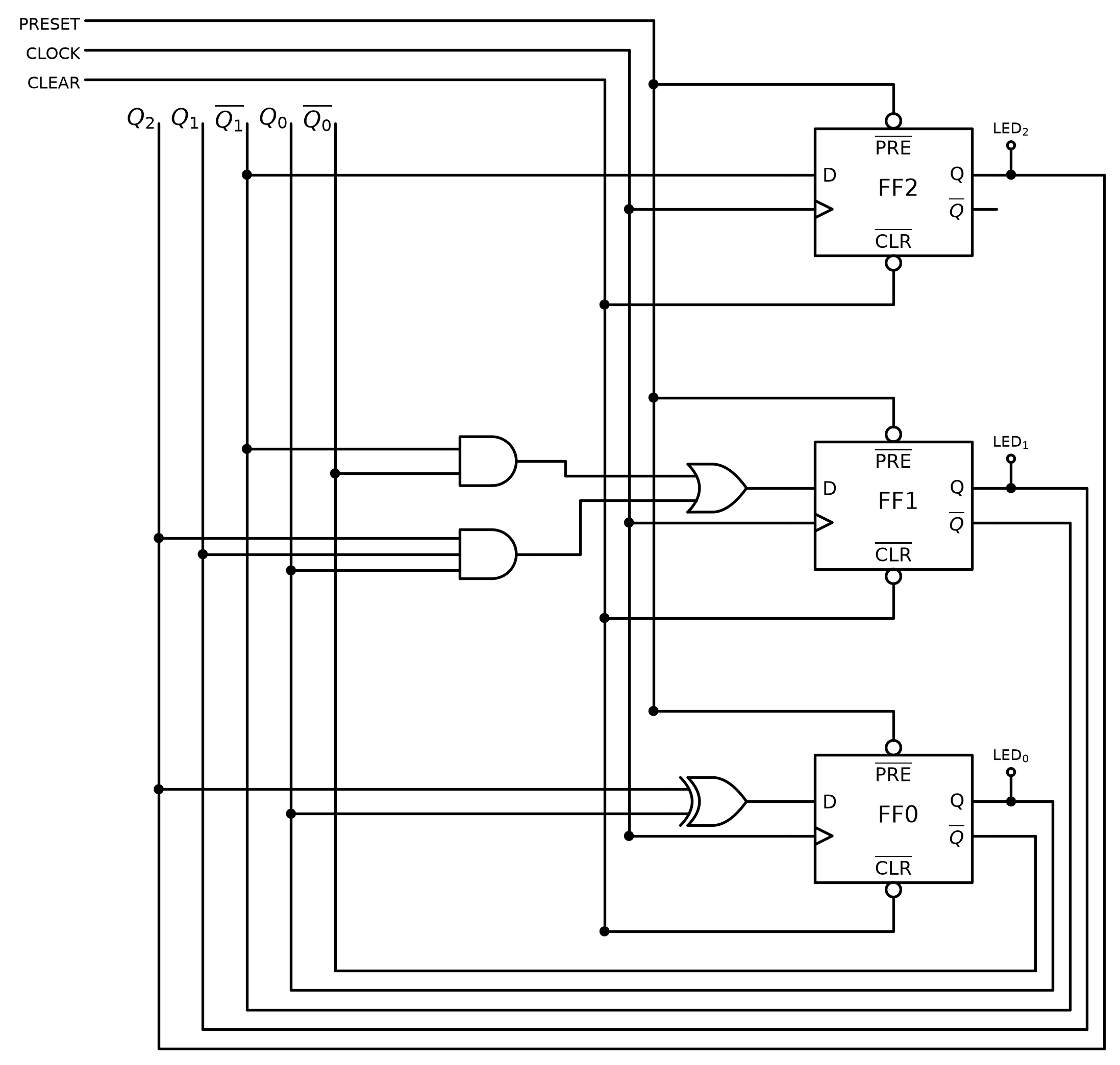
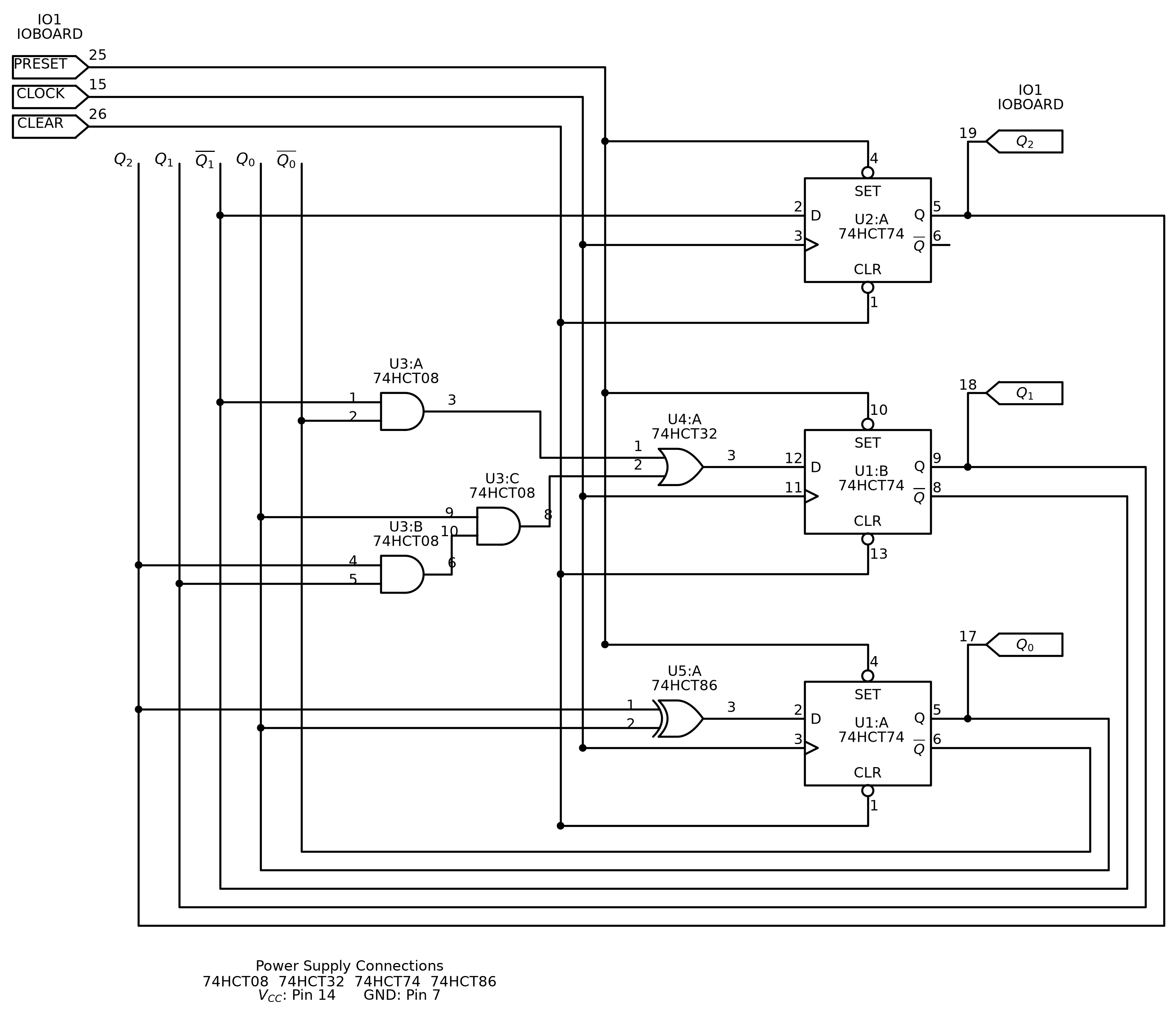
That comes to five 2-input gates across five chips. The breadboard only fits six, so this leaves one spare. No inverters are needed anywhere: the 74HCT74 gives \(\overline{Q}\) alongside \(Q\), so \(\overline{Q_1}\) and \(\overline{Q_0}\) are free.
Circuit Schematic
Figure 1 is a logic diagram. Figure 2 is the same counter drawn as a circuit schematic (see circuit-schematics), with device IDs, chip types and pin numbers from device-pinouts.
It takes five chips: U1 and U2 are 74HCT74 dual flip-flops, U3 a 74HCT08 (the 3-input product is U3:B and U3:C cascaded, since the kit has no 3-input gate), U4:A a 74HCT32 and U5:A a 74HCT86. On the IO board, CLOCK is button B0, PRESET and CLEAR are switches S0 and S1, and \(Q_2 Q_1 Q_0\) drive LEDs L2, L1 and L0.
Reference material
Binary Conversion Drill
Convert between different number representations. All binary numbers are eight bits.
On the HTML site, fill in the blank with your answer (as a quoted string, e.g. "1A"), then click Run Code on the exercise to check. Reload the page for a new random question. In the PDF, the reference implementation is shown instead (interactive exercises need a browser).
Number base conversion
A random question is generated once per page load using an ojs cell, then passed into the Python exercise cells below via the input cell option – this keeps the question stable across repeated “Run Code” clicks (setup blocks re-run on every evaluation, so randomising there would change the question out from under the learner).
Signed number format conversion
Binary Number Representations
Bits, bytes, and words
- Bit = binary digit (0 or 1).
- Byte = 8 bits, e.g.
01010111. - Modern computers deal with words, usually a power-of-2 number of bytes: 1, 2, 4, or 8 bytes = 8, 16, 32, 64 bits.
Representing whole (unsigned) numbers
Each bit position has a value — a power of 2, increasing from right (least significant) to left (most significant):
| Bit position | 9 | 8 | 7 | 6 | 5 | 4 | 3 | 2 | 1 | 0 |
|---|---|---|---|---|---|---|---|---|---|---|
| Value | 512 | 256 | 128 | 64 | 32 | 16 | 8 | 4 | 2 | 1 |
Binary → decimal: add the values of each position where the bit is 1. E.g. 10010001 = \(128 + 16 + 1 = 145\).
- Least significant bit (LSB) — the bit position worth the least (\(2^0 = 1\)).
- Most significant bit (MSB) — the bit position worth the most. For an \(n\)-bit unsigned word, the MSB is worth \(2^{n-1}\).
Converting decimal to binary
Two equivalent methods (example: convert 53 to binary):
- Method 1: rewrite \(n\) as a sum of powers of 2, by repeatedly subtracting the largest power of 2 not greater than \(n\). Assemble the binary number from 1’s in the bit positions corresponding to those powers of 2, 0’s elsewhere.
- Method 2 (build up from the right/LSB): divide \(n\) by 2; the remainder (0 or 1) is the next bit; repeat with \(n\) = the quotient, until \(n = 0\).
Number range (unsigned)
- Smallest representable value: all 0’s → 0.
- Largest representable value: all 1’s → for an \(n\)-bit word, \(2^n - 1\) (e.g. 255 for 8 bits).
Other radices
Radix = number system base. A radix-\(k\) number system has \(k\) distinct symbols for digits \(0\) to \(k-1\), and the value of each digit (from the right) is \(k^0, k^1, k^2, \dots\)
- Octal (radix-8): symbols
0–7. One octal digit corresponds to exactly 3 bits. - Hexadecimal (radix-16): symbols
0–9,A–F. One hex digit corresponds to exactly 4 bits — very convenient for grouping binary.
| Dec | 0 | 1 | 2 | 3 | 4 | 5 | 6 | 7 | 8 | 9 | 10 | 11 | 12 | 13 | 14 | 15 | 16 | 17 |
|---|---|---|---|---|---|---|---|---|---|---|---|---|---|---|---|---|---|---|
| Oct | 0 | 1 | 2 | 3 | 4 | 5 | 6 | 7 | 10 | 11 | 12 | 13 | 14 | 15 | 16 | 17 | 20 | 21 |
| Hex | 0 | 1 | 2 | 3 | 4 | 5 | 6 | 7 | 8 | 9 | A | B | C | D | E | F | 10 | 11 |
Radix notation conventions
Since a bare number like 101 or 747 is ambiguous, a radix indicator is needed. A subscript works generically (e.g. \(101_2\), \(101_{16}\)); in code/assembly, conventions vary:
| Radix | Convention | Example | Where used |
|---|---|---|---|
| Hex | leading 0x |
0x101 |
C, Atmel AVR |
| Hex | trailing h |
101h |
some assembly languages |
| Hex | leading $ |
$747 |
Atmel AVR assembly |
| Octal | leading 0 |
0101 |
C, Atmel AVR |
| Octal | trailing q |
101q |
some assembly languages |
| Octal | leading @ |
@747 |
some assembly languages |
| Binary | leading 0b |
0b101 |
Atmel AVR assembly, some C |
| Binary | trailing b |
101b |
some assembly languages |
| Binary | leading % |
%101 |
some assembly languages |
Boolean Algebra
Logic functions can be expressed as expressions of variables (literals, e.g. \(A, B, X\)) and functions (e.g. \(+, \cdot, \oplus, \bar{\ }\)). Variables and functions can only take values 0 or 1.
Notation conventions
- Inversion: overline, e.g. \(\text{NOT}(A) = \bar A\) (“A bar”).
- AND: dot, or implied by adjacency, e.g. \(\text{AND}(A,B) = AB = A \cdot B\).
- OR: plus sign, e.g. \(\text{OR}(A,B,C) = A+B+C\).
- Other examples: \(\text{XOR}(A,B) = A \oplus B = \bar A B + A \bar B\); \(\text{NAND}(A,B,C) = \overline{ABC}\); \(\text{NOR}(A,B) = \overline{A+B}\).
Boolean identities
| Name | AND form | OR form |
|---|---|---|
| Identity law | \(1A = A\) | \(0 + A = A\) |
| Null law | \(0A = 0\) | \(1 + A = 1\) |
| Idempotent law | \(AA = A\) | \(A + A = A\) |
| Inverse law | \(A\bar A = 0\) | \(A + \bar A = 1\) |
| Commutative law | \(AB = BA\) | \(A + B = B + A\) |
| Associative law | \((AB)C = A(BC)\) | \((A+B)+C = A+(B+C)\) |
| Distributive law | \(A + BC = (A+B)(A+C)\) | \(A(B+C) = AB + AC\) |
| Absorption law | \(A(A+B) = A\) | \(A + AB = A\) |
| De Morgan’s law | \(\overline{AB} = \bar A + \bar B\) | \(\overline{A+B} = \bar A \bar B\) |
De Morgan’s law also means AND and OR gates can be interchanged if you invert all the inputs and the output — this is why NAND/NOR-only circuits (see logic-gates) can implement any function.
Sum of products
Any logic function can be implemented as the OR of AND combinations of its inputs (a sum of products):
- For each row where the truth table output is 1, write the AND term of the inputs (complementing wherever the input is 0) that produces that row.
- OR all of those terms together.
This always works, but doesn’t necessarily give the minimum number of gates — the resulting expression can often be simplified further using the identities above. E.g. \(Z = AB + AC = A(B+C)\) (distributive law) uses fewer gates than the raw sum-of-products form.
Circuit Schematics
A logic diagram shows the idea of a circuit and is hardware-independent (see logic-gates). A circuit schematic goes further: it tells you how to actually build the circuit on real hardware — labelled ICs, pin numbers, power connections — so it’s hardware-specific. Schematics are drawn for practicals and assessment using 74-series logic chips and the CSSE2010/CSSE7201 IO Board (see device-pinouts for pin layouts).
Source: CSSE2010/CSSE7201 - Guide to Drawing Circuit Schematics (Blackboard, v2.3). The rules below are that document’s requirements; the errors are its annotated bad-schematic example.
Required elements
Every circuit schematic must show:
- Labelled inputs and outputs — every input/output needs a sensible, unique name. Inputs and outputs use different arrow symbols (which way they point), and by convention inputs are drawn on the left, outputs on the right.
- Labelled devices — each physical device (chip or IO board) gets a unique identifier: one or more letters for the device type, then a sequential number starting from 1.
- Logic chips:
U1,U2,U3, … - IO board:
IO1(IO2for a second board, etc.) — when a group of inputs/outputs all belong to the same IO board, it only needs to be labelled once for the whole group, not per signal.
- Logic chips:
- Gate labels within a chip — where a chip contains multiple gates, each gate is labelled
A,B,C, … after the chip ID, separated by a colon (e.g.U1:A,U1:B). Labels can be assigned to gates in any order. A chip with only one gate/device doesn’t need a gate letter (justU3). - Device type — written on the line below the device ID (e.g.
74HCT00,74HCT04,IOBOARD). - Pin numbers — every pin used must be numbered per the actual device pinout (see device-pinouts).
- Power supply connections — shown once per device type, not per individual chip. Where two+ chip types share the same power pins, they can be grouped together. The IO board doesn’t need power connections shown.
Common errors
From the guide’s worked example of a bad schematic:
- Duplicate names — two inputs given the same name (e.g. both called
A). Every input needs a unique name. - Missing junction dots — where wires join or split, a dot must mark the connection. Wires that merely cross on the page, with no dot, are not electrically connected.
- Gate label exceeds chip capacity — e.g. labelling a gate
U1:Eon a 74HCT00, which only has four 2-input NAND gates (A–D). A fifth gate needs a new chip ID (U2:A). - Wrong device for the gate type — a different gate type (e.g. NOT vs NAND) needs its own chip identifier; you can’t add it under an existing chip’s ID.
- Reusing pin numbers — e.g.
U1:Cusing the same pins asU1:A. You can’t use the same physical gate twice. - Inconsistent device type — every gate labelled
U1:somethingmust show the same chip type; a chip ID can’t switch part-way through (e.g.U1:Dshown as a 74HCT47 when the rest ofU1is a 74HCT00). - Output errors — two distinct mistakes to watch for:
- Using the input-arrow symbol where an output-arrow symbol is needed.
- Wiring a gate output directly into another output pin/signal — an input should never be tied straight to a gate’s output; gate outputs should only feed output devices (e.g. LEDs) or the inputs of other gates. Doing this may destroy the device.
Combinational Logic Blocks
Reference note for the standard combinational building blocks: the adder-subtractor, the multiplexer, and the decoder. See logic-gates for the gate symbols/truth tables and boolean-algebra for the notation used below.
What makes a circuit combinational
A combinational circuit is a combination of logic gates with \(n\) inputs and \(m\) outputs:
- Each output can be expressed as a function of the \(n\) input variables.
- The output depends on the current inputs only — there is no memory of previous inputs. (Contrast with sequential-circuits, where the output also depends on stored state.)
- It can always be written as a truth table with \(n\) input columns, \(m\) output columns, and \(2^n\) rows (one per possible input combination).
Binary subtraction
\(A - B\) is usually implemented as \(A + (-B)\), where:
- \(A\) and \(B\) are multi-bit quantities;
- “+” here means addition, not OR;
- \(-B\) means the two’s complement of \(B\) (see binary-number-representations).
The two’s complement of \(B\) is calculated by flipping all the bits and adding 1. So a subtractor is just an adder with two extra pieces: something that conditionally inverts \(B\), and something that adds the extra 1.
The controlled inverter (XOR trick)
We need a gate that flips a bit only sometimes: given a mode bit \(M\),
\[Z = \bar B \text{ when } M = 1, \qquad Z = B \text{ when } M = 0\]
The slide poses this as a question and is otherwise blank. Derived from the XOR truth table: XOR with one input held at 0 passes the other input through unchanged, and XOR with one input held at 1 inverts it. So the gate is a 2-input XOR:
\[Z = B \oplus M\]
| M | B | \(Z = B \oplus M\) | Effect |
|---|---|---|---|
| 0 | 0 | 0 | pass through |
| 0 | 1 | 1 | pass through |
| 1 | 0 | 1 | invert |
| 1 | 1 | 0 | invert |
This is called a controlled inverter.
Adder-subtractor circuit
A 4-bit adder-subtractor is built from a 4-bit binary adder (a ripple-carry adder — see 2026-08-04-binary-arithmetic) plus four XOR gates:
- Data input \(A\) (\(A_0 \ldots A_3\)) goes straight into the adder’s \(A\) inputs.
- Data input \(B\) (\(B_0 \ldots B_3\)) goes into the adder’s \(B\) inputs via one XOR gate per bit; the second input of every XOR gate is the shared mode select line \(M\).
- \(M = 0\) means add, \(M = 1\) means subtract.
- The adder produces the data output \(S_0 \ldots S_3\), plus a carry-out \(C_4\) and taking a carry-in \(C_0\).
What should the carry-in be? The slide asks this and leaves it blank. Derived: with \(M = 1\) the XOR gates supply \(\bar B\), and two’s complement needs \(\bar B + 1\) — the extra \(+1\) is supplied by feeding it in as the carry-in. With \(M = 0\) we want plain addition, which needs a carry-in of 0. Both cases are satisfied by
\[C_0 = M\]
so the mode select line is wired to both the XOR gates and the adder’s carry-in.
A 4-bit adder is available as an off-the-shelf IC — the 74HCT283, see device-pinouts.
Multiplexer (mux)
A multiplexer has:
- \(2^n\) data inputs,
- 1 output,
- \(n\) control (or select) inputs, which select one of the data inputs to be “sent” or “steered” to the output.
4-to-1 multiplexer
Data inputs \(D_0 \ldots D_3\), select inputs \(S_1 S_0\), output \(F\). The logic symbol is the characteristic trapezoid with the data inputs on the wide (left) edge, \(F\) on the narrow (right) edge, and the select inputs entering the bottom.
Function table:
| \(S_1\) | \(S_0\) | \(F\) |
|---|---|---|
| 0 | 0 | \(D_0\) |
| 0 | 1 | \(D_1\) |
| 1 | 0 | \(D_2\) |
| 1 | 1 | \(D_3\) |
Note this is a function table, not a full truth table — the full truth table would need \(2^6 = 64\) rows for the six inputs \(S_1, S_0, D_0, D_1, D_2, D_3\).
4-to-1 mux logic circuit implementation
- \(S_1\) and \(S_0\) each feed an inverter, giving \(\bar S_1\) and \(\bar S_0\) as well as the true forms.
- Four 3-input AND gates, one per data input. Each AND gate takes its data input plus the select-literal pair that identifies it: \(D_0\) with \(\bar S_1 \bar S_0\), \(D_1\) with \(\bar S_1 S_0\), \(D_2\) with \(S_1 \bar S_0\), \(D_3\) with \(S_1 S_0\).
- The four AND outputs feed a single 4-input OR gate whose output is \(F\).
That is exactly the sum-of-products form:
\[F = D_0 \bar S_1 \bar S_0 + D_1 \bar S_1 S_0 + D_2 S_1 \bar S_0 + D_3 S_1 S_0\]
Only the AND gate whose select literals match the current \(S_1 S_0\) can be 1, so exactly one data input reaches the OR gate at a time.
2-to-1 multiplexer
Data inputs \(D_0\) and \(D_1\), one control input \(S_0\), output \(F\).
Function table:
| \(S_0\) | \(F\) |
|---|---|
| 0 | \(D_0\) |
| 1 | \(D_1\) |
Expanded to a full truth table over all three inputs:
| \(S_0\) | \(D_0\) | \(D_1\) | \(F\) |
|---|---|---|---|
| 0 | 0 | 0 | 0 |
| 0 | 0 | 1 | 0 |
| 0 | 1 | 0 | 1 |
| 0 | 1 | 1 | 1 |
| 1 | 0 | 0 | 0 |
| 1 | 0 | 1 | 1 |
| 1 | 1 | 0 | 0 |
| 1 | 1 | 1 | 1 |
i.e. \(F = D_0 \bar S_0 + D_1 S_0\). When \(S_0 = 0\) the output tracks \(D_0\) and ignores \(D_1\); when \(S_0 = 1\) it tracks \(D_1\) and ignores \(D_0\).
A quad 2-input multiplexer is available as an off-the-shelf IC — the 74HCT157, see device-pinouts.
Using a mux to implement a logic function
Because the data inputs can be tied to constant 0 or 1, an \(n\)-select mux with its selects wired to the function’s variables can implement any function of those \(n\) variables: set data input \(D_i\) to the value the function should take when the selects equal \(i\). See the worked polling question in 2026-08-06-combinational-logic.
Decoder
A decoder converts an \(n\)-bit input to a logic 1 on exactly one of its \(2^n\) outputs (the one whose index equals the input value); all other outputs are 0.
3-to-8 decoder
Inputs \(A, B, C\) (with \(A\) the most significant), outputs \(D_0 \ldots D_7\).
| A | B | C | \(D_0\) | \(D_1\) | \(D_2\) | \(D_3\) | \(D_4\) | \(D_5\) | \(D_6\) | \(D_7\) |
|---|---|---|---|---|---|---|---|---|---|---|
| 0 | 0 | 0 | 1 | 0 | 0 | 0 | 0 | 0 | 0 | 0 |
| 0 | 0 | 1 | 0 | 1 | 0 | 0 | 0 | 0 | 0 | 0 |
| 0 | 1 | 0 | 0 | 0 | 1 | 0 | 0 | 0 | 0 | 0 |
| 0 | 1 | 1 | 0 | 0 | 0 | 1 | 0 | 0 | 0 | 0 |
| 1 | 0 | 0 | 0 | 0 | 0 | 0 | 1 | 0 | 0 | 0 |
| 1 | 0 | 1 | 0 | 0 | 0 | 0 | 0 | 1 | 0 | 0 |
| 1 | 1 | 0 | 0 | 0 | 0 | 0 | 0 | 0 | 1 | 0 |
| 1 | 1 | 1 | 0 | 0 | 0 | 0 | 0 | 0 | 0 | 1 |
(The slide tabulates only the first four rows and elides the rest with “…”; the remaining four rows are filled in above from the definition — the 1 always sits in the column whose index is the binary value of \(ABC\).)
3-to-8 decoder logic circuit implementation
- Each of \(A\), \(B\), \(C\) is fanned out to an inverter, so all six literals \(A, \bar A, B, \bar B, C, \bar C\) are available on a vertical bus.
- Eight 3-input AND gates, one per output. Each taps the three literals matching its index:
\[D_0 = \bar A \bar B \bar C, \quad D_1 = \bar A \bar B C, \quad D_2 = \bar A B \bar C, \quad D_3 = \bar A B C\] \[D_4 = A \bar B \bar C, \quad D_5 = A \bar B C, \quad D_6 = A B \bar C, \quad D_7 = ABC\]
Each AND gate is the minterm for one input combination, so exactly one is high at any time.
Counters
A counter is a multi-bit register that goes through a determined sequence of states (values) upon the application of input (clock) pulses. It is a [[sequential-circuits|synchronous sequential circuit]] built from [[flip-flops-and-latches|D flip-flops]] plus some combinational logic in the feedback path.
Binary counters
A counter which follows the binary number sequence is a binary counter.
An \(n\)-bit binary counter:
- has \(n\) flip-flops;
- has \(2^n\) different states;
- counts from \(0\) to \(2^n - 1\), then wraps back to \(0\).
For example, a 2-bit binary counter counts
\[00 \to 01 \to 10 \to 11 \to 00 \to \ldots\]
i.e. \(0 \to 1 \to 2 \to 3 \to 0 \to \ldots\)
4-bit binary counter — counting sequence
| Bit 3 | Bit 2 | Bit 1 | Bit 0 | Value |
|---|---|---|---|---|
| 0 | 0 | 0 | 0 | 0 |
| 0 | 0 | 0 | 1 | 1 |
| 0 | 0 | 1 | 0 | 2 |
| 0 | 0 | 1 | 1 | 3 |
| 0 | 1 | 0 | 0 | 4 |
| 0 | 1 | 0 | 1 | 5 |
| 0 | 1 | 1 | 0 | 6 |
| 0 | 1 | 1 | 1 | 7 |
| 1 | 0 | 0 | 0 | 8 |
| 1 | 0 | 0 | 1 | 9 |
| 1 | 0 | 1 | 0 | 10 |
| 1 | 0 | 1 | 1 | 11 |
| 1 | 1 | 0 | 0 | 12 |
| 1 | 1 | 0 | 1 | 13 |
| 1 | 1 | 1 | 0 | 14 |
| 1 | 1 | 1 | 1 | 15 |
| 0 | 0 | 0 | 0 | 0 |
Note how each bit toggles at half the rate of the bit to its right — bit 0 changes every count, bit 1 every second count, bit 2 every fourth, bit 3 every eighth.
Key points
- The next state is a function of the present state (and possibly of external inputs).
- The count sequence can be the binary numbers but does not have to be — if it is, the counter is a binary counter; otherwise it is just some arbitrary cycle through states.
- These circuits are synchronous: all flip-flops share the same clock.
- Asynchronous counters exist too, but are not discussed in this course.
State: the design idea
This is the whole trick, and it is what makes counter design mechanical:
- The values stored in the flip-flops are the current (present) state of the circuit.
- The \(D\) inputs to the flip-flops are the next state — whatever is sitting on \(D\) at the clock edge becomes the new state.
- The \(D\) inputs are some combinational function of the current state (and of any external inputs).
So for a counter with state bits \(Q_{n-1} \ldots Q_1 Q_0\), designing the counter means finding \(n\) Boolean expressions
\[D_i = f_i(Q_{n-1}, \ldots, Q_1, Q_0)\]
and building each one out of gates.
Design recipe
- Write down the count sequence you want, as a cycle of state values.
- Build a present-state / next-state table. One row per possible state — all \(2^n\) of them, not just the ones in your sequence. Columns: present state \(Q_{n-1}\ldots Q_0\), then next state \(D_{n-1}\ldots D_0\). Fill each next-state entry by reading off what follows that state in your sequence.
- Handle unused states. If your sequence doesn’t use all \(2^n\) states, the next state for the unused ones is a don’t-care (X). You may set each X to whatever makes the algebra simplest — but check afterwards where the unused state actually goes, because a self-correcting counter (one whose unused states lead back into the cycle) is nicer than one that can get stuck.
- Read each \(D\) column as a Boolean function of the \(Q\)s. The table is a truth table with the \(Q\)s as inputs and \(D_i\) as the output, so write it in sum-of-products form: OR together one AND term per row where \(D_i = 1\). See boolean-algebra.
- Simplify each expression using the Boolean algebra laws (and the don’t-cares), then draw the circuit: the combinational logic for \(D_i\) feeding flip-flop \(i\), with every flip-flop on a common clock. See circuit-schematics for schematic conventions and device-pinouts for the 74HCT74 / 74HCT175 D flip-flop packages.
The smallest case falls straight out of the recipe: a 1-bit counter counts \(0 \to 1 \to 0 \to \ldots\), so its next state is always the complement of its present state, giving \(D = \bar Q\) — a single flip-flop with its \(\bar Q\) output wired back to its own \(D\) input (a toggle).
Worked example — a 2-bit counter for \(00 \to 10 \to 01 \to 00\)
Note
This example is posed on the lecture slides but left blank (“to be worked through in class”). The derivation below is reconstructed, not copied from the slides.
Step 1–2 — present-state / next-state table. The sequence uses three of the four states; \(11\) is unused, so its next state is a don’t-care.
| \(Q_1\) | \(Q_0\) | \(D_1\) | \(D_0\) | comment |
|---|---|---|---|---|
| 0 | 0 | 1 | 0 | \(00 \to 10\) |
| 0 | 1 | 0 | 0 | \(01 \to 00\) |
| 1 | 0 | 0 | 1 | \(10 \to 01\) |
| 1 | 1 | X | X | unused state |
Step 4 — read off the columns.
\(D_1\) is 1 only in the row \(Q_1Q_0 = 00\). Making the don’t-care 1 would give \(Q_1 \odot Q_0\) (XNOR), which is no simpler, so take the don’t-care as 0:
\[D_1 = \bar Q_1 \bar Q_0\]
\(D_0\) is 1 only in the row \(Q_1Q_0 = 10\), which gives \(D_0 = Q_1\bar Q_0\). Here the don’t-care does help: setting it to 1 makes \(D_0 = 1\) for both rows with \(Q_1 = 1\), so
\[D_0 = Q_1\]
Step 5 — the circuit. Two D flip-flops on a common clock. Flip-flop 0’s \(D\) input is wired directly to flip-flop 1’s \(Q_1\) output — no gate at all. Flip-flop 1’s \(D\) input is driven by a 2-input NOR of \(Q_1\) and \(Q_0\) (since \(\bar Q_1 \bar Q_0 = \overline{Q_1 + Q_0}\)), or equivalently by an AND of the two \(\bar Q\) outputs.
Check, including the unused state:
| present | \(D_1 D_0\) | next |
|---|---|---|
| 00 | 1 0 | 10 |
| 10 | 0 1 | 01 |
| 01 | 0 0 | 00 |
| 11 | 0 1 | 01 |
The cycle is right, and the unused state \(11\) falls into the cycle at \(01\) on the next clock edge, so the counter is self-correcting. (Choosing \(D_0 = Q_1\bar Q_0\) instead — don’t-care set to 0 — would send \(11 \to 00\), also fine, at the cost of one more gate input.)
Applied exercise
week4-lab-lab-7-exercises is exactly this recipe at \(n = 3\): design a 3-bit synchronous counter that steps through an allocated 7-state sequence, with the eighth (missing) state treated as a don’t-care.
Device Pinouts
Pin numbers for the 74-series logic chips and IO board used in circuit-schematics. All quad 2-input gate chips (74HCT00, 08, 32, 86) share the same pin layout — only the gate function differs.
Source: CSSE2010/CSSE7201 Device Pinouts and Symbols (Blackboard, v4). This is the whole parts list: every gate chip in it is 2-input (plus the hex inverter), so a design needing a 3-or-more-input gate has to be built up from 2-input ones. There is no 3-input AND/OR/NAND in the kit.
Power and ground
Power/ground connections are shown separately from gate pins on a schematic (see circuit-schematics): logic high/power uses a VCC symbol, logic low/ground uses a ground symbol.
Quad 2-input gates (74HCT00 / 08 / 32 / 86)
| Chip | Function | Gate A | Gate B | Gate C | Gate D | VCC | GND |
|---|---|---|---|---|---|---|---|
| 74HCT00 | Quad 2-input NAND | in 1,2 → out 3 | in 4,5 → out 6 | in 9,10 → out 8 | in 12,13 → out 11 | 14 | 7 |
| 74HCT08 | Quad 2-input AND | in 1,2 → out 3 | in 4,5 → out 6 | in 9,10 → out 8 | in 12,13 → out 11 | 14 | 7 |
| 74HCT32 | Quad 2-input OR | in 1,2 → out 3 | in 4,5 → out 6 | in 9,10 → out 8 | in 12,13 → out 11 | 14 | 7 |
| 74HCT86 | Quad 2-input XOR | in 1,2 → out 3 | in 4,5 → out 6 | in 9,10 → out 8 | in 12,13 → out 11 | 14 | 7 |
74HCT04 — Hex inverter
Six independent NOT gates. VCC = pin 14, GND = pin 7.
| Gate | A | B | C | D | E | F |
|---|---|---|---|---|---|---|
| in → out | 1→2 | 3→4 | 5→6 | 9→8 | 11→10 | 13→12 |
74HCT74 — Dual D-type flip-flop (14-pin)
| Pin | 1 | 2 | 3 | 4 | 5 | 6 | 7 | 8 | 9 | 10 | 11 | 12 | 13 | 14 |
|---|---|---|---|---|---|---|---|---|---|---|---|---|---|---|
| Signal | CLR1 | D1 | CLK1 | SET1 | Q1 | \(\overline{Q1}\) | GND | \(\overline{Q2}\) | Q2 | SET2 | CLK2 | D2 | CLR2 | VCC |
Set and clear inputs can be omitted from the schematic if not needed.
74HCT157 — Quad 2-input multiplexer (16-pin)
| Pin | 1 | 2 | 3 | 4 | 5 | 6 | 7 | 8 | 9 | 10 | 11 | 12 | 13 | 14 | 15 | 16 |
|---|---|---|---|---|---|---|---|---|---|---|---|---|---|---|---|---|
| Signal | SEL | A0 | B0 | Y0 | A1 | B1 | Y1 | GND | Y2 | B2 | A2 | Y3 | B3 | A3 | ENABLE | VCC |
74HCT175 — Quad D-type flip-flop (16-pin)
| Pin | 1 | 2 | 3 | 4 | 5 | 6 | 7 | 8 | 9 | 10 | 11 | 12 | 13 | 14 | 15 | 16 |
|---|---|---|---|---|---|---|---|---|---|---|---|---|---|---|---|---|
| Signal | CLR | Q0 | \(\overline{Q0}\) | D0 | D1 | Q1 | \(\overline{Q1}\) | GND | CLK | Q2 | \(\overline{Q2}\) | D2 | D3 | Q3 | \(\overline{Q3}\) | VCC |
74HCT283 — 4-bit full adder (16-pin)
| Pin | 1 | 2 | 3 | 4 | 5 | 6 | 7 | 8 | 9 | 10 | 11 | 12 | 13 | 14 | 15 | 16 |
|---|---|---|---|---|---|---|---|---|---|---|---|---|---|---|---|---|
| Signal | S1 | B1 | A1 | S0 | A0 | B0 | C0 | GND | C4 | S3 | B3 | A3 | S2 | A2 | B2 | VCC |
\(C0\) is the carry-in, \(C4\) the carry-out; \(A_i, B_i\) are the two 4-bit operands and \(S_i\) the 4-bit sum.
IO board
| Pins | Function |
|---|---|
| 1 | TX |
| 2 | RX |
| 3 | SSD cathode |
| 4 | SSD decimal point |
| 5–11 | SSD segments G to A |
| 12–15 | Buttons B3 to B0 |
| 16 | Logic probe |
| 17–24 | LEDs L0 to L7 |
| 25–32 | Switches S0 to S7 |
On a schematic the IO board is labelled IO1 (IO2 for a second board), with inputs using an input-style arrow and outputs an output-style arrow (see circuit-schematics). Use sensible signal names rather than the raw pin labels where possible.
Flip-Flops and Latches
Flip-flops and latches are the storage elements — the circuits that let a design remember a value even after the input that produced it has changed. They’re what turns a combinational circuit into a [[sequential-circuits|sequential circuit]].
The D flip-flop
The D flip-flop is the only flip-flop type covered in this course. Its symbol is a rectangle with:
- D — the data input, on the left.
- Q — the output, on the right.
- CLK — the clock, a control input on the left, drawn with a small triangle where it meets the box.
How it works: Q copies the value of D (and remembers it) whenever CLK goes from 0 to 1 — the rising edge. In between clock edges the flip-flop is not responsive, so it holds the stored value. Q changes only on that 0→1 transition.
Summary: a D flip-flop remembers a single bit — either a “1” or a “0”. It keeps that value until the next clock edge, at which point the D input is transferred to output Q.
- To remember \(n\) bits you need \(n\) D flip-flops.
- An \(n\)-bit register is (by definition) \(n\) D flip-flops. See shift-registers.
- Flip-flops can themselves be made out of logic gates.
Characteristic table
A characteristic table defines the operation of a flip-flop in tabular form. The left column is the input; the right column, \(Q(t+1)\), is what the output will be on the next clock edge (i.e. when CLK goes 0→1).
| D | Q(t+1) | |
|---|---|---|
| 0 | 0 | Reset |
| 1 | 1 | Set |
That is the whole behaviour: the flip-flop is reset (to 0) or set (to 1) according to D, at the clock edge.
Worked waveform
The lecture’s example: D is 0, 0, then 1, 1 across a clock with two rising edges; CLK starts low, pulses high, goes low, then pulses high again after D has risen.
| Clock edge | D at that edge | Q after |
|---|---|---|
| (before the first edge) | — | unknown/undefined |
| 1st rising edge | 0 | 0 |
| 2nd rising edge | 1 | 1 |
Before the first rising edge Q is marked with an “X” on the slide — its value is undefined, because nothing has been clocked in yet. Between the two rising edges Q stays 0 even though D has already risen to 1: the flip-flop is only sensitive at the edge.
Other flip-flop types
Other types exist — JK flip-flops and T flip-flops — but they are not covered in this course. Only the D flip-flop is used.
Latches vs flip-flops
- Latches are level triggered devices — they latch the output and respond to changes of logic levels on the inputs.
- A latch circuit can be modified so that it becomes sensitive to an edge (a momentary transition) of a control input, i.e. a clock signal. Such circuits are called flip-flops.
- A flip-flop can store 1 bit of information while being sensitive to a clock edge — it changes its output only at the clock edges, based on the inputs.
- So: latches are level triggered; flip-flops are edge triggered.
A clock signal has two edges:
| Edge | Transition |
|---|---|
| Positive (rising) edge | 0 → 1 |
| Negative (falling) edge | 1 → 0 |
A D flip-flop can therefore be positive edge triggered or negative edge triggered. In a positive edge triggered D flip-flop, D is copied to Q at the positive edge of the clock; in between clock edges the flip-flop is not responsive, thus stores the value.
The state of a flip-flop is the value it is storing. Flip-flops are more useful than latches in practice.
The SR latch (cross-coupled NOR gates)
Structure: two 2-input NOR gates cross-coupled.
- The top NOR gate takes \(S\) as one input and the bottom gate’s output as its other input; its output is \(\bar Q\).
- The bottom NOR gate takes \(R\) as one input and the top gate’s output (\(\bar Q\)) as its other input; its output is \(Q\).
So each gate’s output feeds back into the other gate’s input — that feedback loop is what stores the bit. Recall (from logic-gates) that a NOR gate outputs 1 only when both inputs are 0; any 1 on an input forces the output to 0.
The truth table on the slide is left blank (“to be completed in class”). Derived from the NOR behaviour and the cross-coupling, assuming a stable starting state \(Q\):
| S | R | Q | \(\bar Q\) | Meaning |
|---|---|---|---|---|
| 0 | 0 | \(Q\) (unchanged) | \(\bar Q\) (unchanged) | Hold — remembers the previous value |
| 0 | 1 | 0 | 1 | Reset — Q forced to 0 |
| 1 | 0 | 1 | 0 | Set — Q forced to 1 |
| 1 | 1 | 0 | 0 | Invalid — see below |
Reasoning for each row:
- \(S=0, R=0\): neither gate is forced. Say \(Q=1\); then the top gate sees \(S=0\) and \(Q=1\), so \(\bar Q = 0\); the bottom gate sees \(R=0\) and \(\bar Q=0\), so \(Q=1\) — consistent. The same argument works with \(Q=0\). Both states are self-consistent, so the latch simply holds whatever it already had.
- \(S=1, R=0\): the top gate has a 1 on an input, so \(\bar Q = 0\). The bottom gate then sees \(R=0\) and \(\bar Q=0\), so \(Q=1\). \(S\) sets the latch.
- \(S=0, R=1\): mirror image — the bottom gate has a 1 on an input, so \(Q=0\); the top gate then sees \(S=0\) and \(Q=0\), so \(\bar Q=1\). \(R\) resets the latch.
- \(S=1, R=1\): both gates have a 1 on an input, so both outputs are 0 — \(Q = \bar Q = 0\). This breaks the whole point of the two outputs being complements, which is why the combination is called forbidden/invalid. What happens after both inputs return to 0 simultaneously is not uniquely determined (the two gates race), so the resulting state is indeterminate. The slide is blank here and the worked answer was only done live — check the lecture recording for the exact form the lecturer wrote in this row.
Homework: latches from NAND gates
Slide 11 is otherwise blank and sets a homework: analyse the S-R latch circuit from the previous slide when the NOR gates are replaced with NAND gates, and complete the truth table.
The slide gives no answer. Derived, keeping the same wiring and the same input labels (top gate: \(S\) and the bottom output; bottom gate: \(R\) and the top output), and recalling that a NAND outputs 0 only when both inputs are 1 — so any 0 on an input forces the output to 1:
| S | R | top output | bottom output | Meaning |
|---|---|---|---|---|
| 1 | 1 | unchanged | unchanged | Hold |
| 0 | 1 | 1 | 0 | bottom output forced to 0 |
| 1 | 0 | 0 | 1 | bottom output forced to 1 |
| 0 | 0 | 1 | 1 | Invalid — outputs no longer complementary |
The headline result: with NAND gates the inputs become active low (the latch holds at \(S=R=1\) rather than \(S=R=0\), and the invalid combination moves to \(S=R=0\)), and with the labels left unchanged the set/reset roles swap over relative to the NOR version. This is why NAND latches are conventionally drawn with the inputs labelled \(\bar S\) and \(\bar R\). Worth confirming against the lecturer’s own labelling.
A real D flip-flop
A real D flip-flop is built from cross-coupled NAND gates — the lecture’s schematic uses six NAND gates. As well as D, CLK and the outputs \(Q\) and \(\bar Q\), it has two extra inputs:
- \(\overline{\text{PRE}}\) (Preset) — forces \(Q\) to 1.
- \(\overline{\text{CLR}}\) (Clear) — forces \(Q\) to 0.
Both are drawn with overbars, i.e. they are active low, and both are asynchronous: they act on the latch directly, independent of the clock, rather than waiting for a clock edge. In the schematic they feed into the NAND gates of the input latches directly, bypassing the D/CLK path.
Symbols used
Four related symbols, all drawn as a rectangle with D in at the top left, Q out at the top right, and a clock input CK at the bottom left. What distinguishes them is the marking on that CK input:
| Symbol | CK input marking | Device | Triggered on |
|---|---|---|---|
| (a) | plain input | Latch | High level of CK |
| (b) | bubble (inversion circle) | Latch | Low level of CK |
| (c) | triangle | Flip-flop | Rising (positive) edge of the clock |
| (d) | bubble + triangle | Flip-flop | Falling (negative) edge of the clock |
The two markings read independently and are the whole key to the notation:
- The triangle indicates edge-triggered, and therefore that the device is a flip-flop rather than a latch. No triangle means level-triggered, i.e. a latch.
- The bubble indicates inversion, i.e. the falling edge (or the low level) rather than the rising edge (or the high level).
The slide only annotates (c) and (d) explicitly; the readings given above for (a) and (b) are derived from those two rules.
D flip-flop chips
- 74HCT74 — dual D flip-flop (two independent D flip-flops in a 14-pin package), each with CLR and PR (preset) inputs and \(Q\)/\(\bar Q\) outputs. Pinout in device-pinouts.
- 74HCT273 — eight D flip-flops in a 20-pin package, so it can hold one byte (8 bits) of information.
The lecture points to the “device symbols PDF on Blackboard” for the full symbol set.
Logic Gates
Every logic gate has one or more inputs and exactly one output, and can be described four equivalent ways: logic symbol, truth table, Boolean expression, timing diagram (see timing-diagrams for the last of these, and for real-gate propagation delay / rise / fall times).
The 7 basic gate types
| Gate | Behaviour | Truth table (\(A,B \to X\)) |
|---|---|---|
| NOT (inverter) | Inverts the input | 0→1, 1→0 |
| AND | \(X=1\) iff all inputs are 1 | 00→0, 01→0, 10→0, 11→1 |
| OR | \(X=1\) iff at least one input is 1 | 00→0, 01→1, 10→1, 11→1 |
| NAND | \(X=1\) iff at least one input is 0 (NOT AND) | 00→1, 01→1, 10→1, 11→0 |
| NOR | \(X=1\) iff all inputs are 0 (NOT OR) | 00→1, 01→0, 10→0, 11→0 |
| XOR | \(X=1\) iff exactly one input is 1 (“odd function”) | 00→0, 01→1, 10→1, 11→0 |
| XNOR | \(X=1\) iff inputs are the same (“even function”) | 00→1, 01→0, 10→0, 11→1 |
Useful to remember: XOR is the odd function, XNOR is the even function — this generalises directly to more than 2 inputs (XOR = 1 iff an odd number of inputs are 1).
Universal (complete) gates
All circuits can be constructed from NAND-only or NOR-only gates — these are called complete (or universal) gates, because NOT, AND, and OR can each be built purely from one gate type:
- NOT: a NAND (or NOR) gate with both inputs tied together.
- AND: two NANDs in series (NAND followed by another NAND used as an inverter), or the NOR equivalent.
- OR: built similarly from NAND-only or NOR-only combinations.
NAND and NOR are preferred in practice because they’re easier to build from transistors than AND/OR directly.
Gates on ICs
Example: the 74HCT00 integrated circuit packages four independent 2-input NAND gates into a single 14-pin DIP chip (Vcc = power e.g. 5V, GND = ground/0V; pin spacing 0.1”×0.3”, chip ~15mm long).
Sequential Circuits
A sequential circuit is a circuit whose output depends not only on the current inputs but also on the values it is currently storing. The storage is done with flip-flops — see flip-flops-and-latches for the storage elements themselves.
Combinational vs sequential
| Combinational | Sequential | |
|---|---|---|
| Contents | Logic gates only (no flip-flops) | Includes flip-flops as well as logic gates |
| Output determined by | The inputs alone — uniquely | Current inputs and current state |
| Repeatability | Same inputs always give the same output | Same inputs can give different outputs, depending on state |
| When output changes | Whenever an input changes | Only when the clock ‘ticks’ |
| Examples | Adders, multiplexers, decoders, demultiplexers, encoders (see combinational-logic-blocks) | Counters, registers (see [counters], shift-registers) |
A combinational example from earlier in the course: \(A\) into one input of an AND gate, \(B\) and \(C\) into an OR gate whose output feeds the AND gate’s other input, giving \(X = A(B+C)\). Nothing in that circuit remembers anything — change \(A\), \(B\) or \(C\) and the output follows immediately (after propagation delay; see timing-diagrams).
The key contrast: if an input to a combinational circuit changes, the output can change too and the previous value is lost forever. A sequential circuit can hold onto a value even after the input that produced it has gone away.
State
- State = the value stored in the flip-flops.
- Output depends on the inputs and the state.
- Next state depends on the inputs and the (present) state.
“Present state” is what the flip-flops hold right now; “next state” is what they will hold after the next clock edge. The combinational logic computes the next state from the present state and the inputs; the flip-flops only adopt it when the clock edge arrives.
General structure of a sequential circuit
The standard block diagram has two blocks and a feedback loop:
- A combinational circuit block (just logic gates). It takes the external inputs plus the feedback from the flip-flops, and produces the external outputs plus the values to be loaded into the flip-flops.
- A flip-flops block (the storage elements). Its data inputs come from the combinational circuit; it also takes clock pulses as a separate control input.
- A feedback path runs from the flip-flops’ outputs back around into the combinational circuit’s inputs. That loop is what makes the circuit sequential — the stored state is fed back in and influences the next output and the next state.
Note that the clock pulses go only to the flip-flops, not to the combinational logic.
Synchronous sequential circuits
In a synchronous sequential circuit the storage elements can only change at discrete instants of time, set by a common clock signal:
- Assume a clock signal — a regularly repeating square wave alternating between 0 and 1.
- The outputs of the storage elements change only on the edges of that control signal.
- Contrast with logic gates, whose outputs change whenever their inputs change.
Because every flip-flop shares the same clock, the whole circuit’s state changes in one step at each clock edge, which is what makes such circuits tractable to design and analyse.
Shift Registers
Registers and shift registers are the simplest useful [[sequential-circuits|sequential circuits]] — groups of [[flip-flops-and-latches|D flip-flops]] sharing a common clock.
Registers
- A register is a group of flip-flops. An \(n\)-bit register consists of \(n\) flip-flops and is capable of storing \(n\) bits.
- A register is a sequential circuit without any combinational logic — it is just the storage elements and their shared control lines.
- Registers are used to store binary information (data/instructions) inside a processor.
Structure of the 4-bit register example (Mano, Digital Design, 3rd ed.):
| Signal | Connection |
|---|---|
| \(I_0 \ldots I_3\) | the four parallel data inputs, one to each flip-flop’s \(D\) input |
| \(A_0 \ldots A_3\) | the four parallel outputs, taken from each flip-flop’s \(Q\) |
Clock |
a single common line driven to the \(C\) (clock) input of all four flip-flops |
Clear |
a single common line driven to the \(R\) (reset) input of all four flip-flops, drawn active-low (bubble on the input) |
So on each rising clock edge all four flip-flops simultaneously capture their \(I\) inputs; asserting Clear forces all four outputs to 0 asynchronously (see flip-flops-and-latches for asynchronous SET/CLR).
Shift registers
A shift register is a register which is capable of shifting its binary information in one or both directions.
The 4-bit shift register example is built as a chain: the serial input \(SI\) feeds the \(D\) input of the first flip-flop; each flip-flop’s \(Q\) output feeds the next flip-flop’s \(D\) input; the last flip-flop’s \(Q\) is the serial output \(SO\). All four flip-flops share a common \(CLK\) line.
On each rising clock edge every stored bit moves one place along the chain, the bit currently on \(SI\) enters the first stage, and the bit that was in the last stage leaves at \(SO\).
Worked through by hand, with stages labelled \(Q_0\) (nearest \(SI\)) through \(Q_3\) (= \(SO\)), starting from all zeros and shifting in the bit sequence 1, 0, 1, 1:
| Clock edge | \(SI\) | \(Q_0\) | \(Q_1\) | \(Q_2\) | \(Q_3\) (\(=SO\)) |
|---|---|---|---|---|---|
| (initial) | — | 0 | 0 | 0 | 0 |
| 1 | 1 | 1 | 0 | 0 | 0 |
| 2 | 0 | 0 | 1 | 0 | 0 |
| 3 | 1 | 1 | 0 | 1 | 0 |
| 4 | 1 | 1 | 1 | 0 | 1 |
After 4 clock edges the 4 serially-supplied bits sit in the 4 flip-flops, and one further edge would push the first of them out of \(SO\).
Serial ↔︎ parallel conversion
Shift registers can be used to do serial-to-parallel conversion, and vice versa. This is the reason they show up everywhere data has to travel over a single wire but be used a word at a time.
- Serial in, parallel out: drive the bits one per clock edge into \(SI\); after \(n\) edges, the \(n\) flip-flop \(Q\) outputs — read as a group — are the parallel word. This is exactly the table above: clock 4 bits in, then read \(Q_0 Q_1 Q_2 Q_3\) in parallel.
- Parallel in, serial out: load the \(n\) bits into the flip-flops in one clock edge (a parallel load — see below), then clock \(n\) more times, reading one bit per edge off \(SO\).
Note
The lecture slide for this figure is blank and marked “figure to be completed in class”. The description above is derived from the standard construction: the parallel outputs are simply the \(Q\) pins of the flip-flops already present in the 4-bit shift register, brought out as a group.
Parallel load vs serial shift
A plain shift register can only be filled one bit per clock. To also allow parallel load — all \(n\) bits written at once from \(n\) parallel inputs — each flip-flop’s \(D\) input is fed from a 2-to-1 multiplexer (see combinational-logic-blocks) instead of directly from the previous stage:
| Mux select | Mux data input chosen | Effect on that stage |
|---|---|---|
| “shift” | the previous stage’s \(Q\) (or \(SI\) for the first stage) | serial shift by one place |
| “load” | that stage’s parallel data input \(I_i\) | parallel load of the whole word in one clock edge |
The select line is common to all the muxes, so on each clock edge the register either shifts by one place or loads the whole parallel word.
Note
The lecture slide for this figure is also blank and marked “figure to be completed in class”, so the exact drawing done in the lecture is not recoverable from the deck. The mux-per-flip-flop construction above is derived, and is confirmed by the following slide, which refers back to “the same multiplexer concept”.
The mux-based bidirectional shift element
The lecture gives a single building block for a shift register that shifts in either direction:
- a 2-to-1 multiplexer whose output drives the \(D\) input of one D flip-flop;
- the mux’s select line is a control signal called DIRN;
- DIRN = 0 selects mux input 0 → left shift;
- DIRN = 1 selects mux input 1 → right shift;
- the flip-flop’s \(Q\) is that stage’s output, and the flip-flop is clocked from the common clock.
Chaining \(n\) of these elements and wiring, for each stage, mux input 0 to the neighbour on the left-shift side and mux input 1 to the neighbour on the right-shift side gives an \(n\)-bit bidirectional shift register: one shared DIRN line decides which way the whole register shifts on the next clock edge.
For a 3-bit register with bits \(Q_2 Q_1 Q_0\) (\(Q_2\) most significant), taking left shift to mean bits move towards the more-significant end:
| Stage | Mux input 0 (DIRN=0, left shift) | Mux input 1 (DIRN=1, right shift) |
|---|---|---|
| \(Q_2\) | \(Q_1\) | \(SI_R\) (serial input for right shifts) |
| \(Q_1\) | \(Q_0\) | \(Q_2\) |
| \(Q_0\) | \(SI_L\) (serial input for left shifts) | \(Q_1\) |
One clock edge applied to a 3-bit register holding \(Q_2 Q_1 Q_0 = 110\), with both serial inputs held at 0:
| DIRN | Operation | Before (\(Q_2Q_1Q_0\)) | After (\(Q_2Q_1Q_0\)) |
|---|---|---|---|
| 0 | left shift | 110 | 100 |
| 1 | right shift | 110 | 011 |
The physical layout drawn in class is not in the slides; the derivation above is the standard construction. See 2026-08-13-shift-registers for the exercise as it was set.
Universal shift register
A universal shift register is the combination of all of the above capabilities in one device: it can hold its value, shift left, shift right, and be parallel-loaded, with the operation selected by control inputs.
Warning
The “Universal Shift Register” slide in the lecture deck is entirely blank — the title only. The one-line description above is the standard definition; everything specific (the control encoding, the mux width, the figure) was covered in class and is not in the slides.
Wide (multi-bit) shift registers
A shift register does not have to shift one bit at a time — it can shift a whole multi-bit word per clock edge. The lecture’s example is an 8-bit wide, 4-stage queue:
- four registers in a row, each 8 bits wide (inputs labelled \(A\) through \(H\), outputs labelled \(Q_1\) through \(Q_8\));
- the 8-bit
Inputbus feeds the first register’s 8 data inputs; - each register’s 8 \(Q\) outputs feed the next register’s 8 data inputs, as a bus;
- the last register’s outputs are the 8-bit
Output; - all four registers share a common clock line, and each has an
ENB(enable) input.
Functionally this is the same chain as the 1-bit shift register, but each “stage” holds a byte rather than a bit — so it behaves as a 4-deep queue of bytes: a byte presented at Input appears at Output four clock edges later.
Timing Diagrams
A timing diagram is the fourth of the four equivalent ways to describe a logic function, alongside the logic symbol, the truth table, and the Boolean expression (see logic-gates).
Timing diagram as a logic representation
It is like a truth table, but in graphical format: time runs left to right along the horizontal axis, and each signal gets its own horizontal track that steps between the logic 0 and logic 1 levels (drawn as two dashed reference lines).
Worked example — an inverter. The input waveform starts at logic 0, rises to logic 1 for a period, then falls back to logic 0. The output waveform is the mirror image: it starts at logic 1, falls to logic 0 for exactly that period, then returns to logic 1. Each change in the input causes the output to change.
Convention for drawing the input waveforms
The input waveforms must be drawn so that all possible input combinations are covered — that is what makes the diagram equivalent to the full truth table.
The standard construction for a 2-input gate divides the time axis into four equal intervals and drives the inputs like a binary count:
- \(A\) is low for the first half of the diagram, then high for the second half.
- \(B\) toggles at twice that rate: low, high, low, high.
Reading the four intervals left to right therefore gives \(AB = 00, 01, 10, 11\) — every combination, once each, in truth-table order. For \(n\) inputs the same scheme generalises: input \(i\) toggles at half the rate of input \(i+1\), and the diagram is \(2^n\) intervals wide.
To read a gate’s output off the diagram, work interval by interval: identify the \(AB\) combination in that interval, look up the gate’s truth table row, and draw the output at that level for the width of the interval.
Real gates aren’t perfect: the reality of timing
The idealised diagrams above show instantaneous, perfectly square transitions. Real gates do not behave that way — real waveforms have sloped edges, and the output changes some time after the input does. Three quantities describe this:
| Term | Definition |
|---|---|
| Propagation delay | Time for a change in the input to affect the output. |
| Fall time | Time taken for the output to fall from 1 to 0. |
| Rise time | Time for the output to rise from 0 to 1. |
Measured on an inverter: the input ramps up, and only after the propagation delay does the output begin to move; the output’s downward edge then takes the fall time to complete, and its later upward edge takes the rise time.