AVR I/O Ports
How an AVR program actually reads a switch and lights an LED: the I/O register file, the three registers behind every port, the two instructions that reach them, how to change one bit of a port without disturbing the others, what writing to PINx really does, and the pins’ alternate uses by the serial interfaces. See avr-architecture for the chip these live on, avr-instructions for the instruction set, and io-board for the devices that get wired to the pins.
I/O registers
The ATmega324A has 224 I/O registers — registers that control the peripherals and carry data to and from them:
- Timers and counters
- Analog to digital converters
- Serial input/output
- General purpose input/output ports
They are not the general purpose registers. Some instructions work with these, others with r0–r31, and confusing the two is the standard beginner error — ldi r16, 0xFF and out DDRA, r16 name completely different register files with the same-looking numbers.
Some addresses are reserved (not actually available on this device). The full list is the I/O register summary, pages 636 to 639 of the datasheet.
Where they live, and how you get at them
I/O registers 0 to 223 sit in the data address space at memory addresses 32 to 255 (0x20 to 0xFF) — see memory-models for why the AVR has a separate data space at all. That gives two ways to name the same register, and two names for it:
| Range | Reached by | |
|---|---|---|
| First 64 I/O registers (0 to 63) | data addresses 0x20–0x5F |
in and out and ld/st |
| Other 160 — the “extended” I/O registers (64 to 223) | data addresses 0x60–0xFF |
ld/st only |
so the two numbering systems differ by a constant:
\[\text{data memory address} = \text{I/O register number} + \texttt{0x20}\]
The offset is exactly the 32 general purpose registers, which occupy 0x0000–0x001F at the bottom of the data space ahead of them.
Why the split exists at all: in/out encode the I/O register number in six bits of the instruction word, and \(2^6 = 64\). Everything past register 63 has no room in the encoding, so it can only be reached the long way round, by its data address.
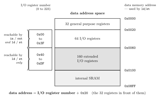
Figure 1: The bottom of the ATmega324A data address space, and the two numbering systems that live on it. Every I/O register has two numbers — its I/O register number (what in/out take) and its data memory address (what ld/st take) — and they differ by a constant 0x20, because the 32 general purpose registers sit in front of them in the same space. Only the first 64 I/O registers have an I/O register number small enough to fit the six operand bits of in/out; the 160 extended ones can be reached by their data address alone. The map follows the convention of csse2010-diagram-notation: lowest address at the top, hex addresses outside.
Extract from the I/O register list
The general purpose port registers are the first twelve entries, in the order PIN, DDR, PORT for each port in turn:
| Data address | I/O reg number | Name |
|---|---|---|
0x2B |
0x0B |
PORTD |
0x2A |
0x0A |
DDRD |
0x29 |
0x09 |
PIND |
0x28 |
0x08 |
PORTC |
0x27 |
0x07 |
DDRC |
0x26 |
0x06 |
PINC |
0x25 |
0x05 |
PORTB |
0x24 |
0x04 |
DDRB |
0x23 |
0x03 |
PINB |
0x22 |
0x02 |
PORTA |
0x21 |
0x01 |
DDRA |
0x20 |
0x00 |
PINA |
Further up the same list, to show the pattern continues and that reserved entries are real:
| Data address | I/O reg number | Name |
|---|---|---|
0x38 |
0x18 |
TIFR3 |
0x37 |
0x17 |
TIFR2 |
0x36 |
0x16 |
TIFR1 |
0x35 |
0x15 |
TIFR0 |
0x34 |
0x14 |
Reserved |
Read the two columns carefully in an exam question. out 0x02, r16 writes PORTA, but sts 0x02, r16 writes general purpose register r2 — the same number, two address spaces, and only the instruction tells them apart.
GPIO ports
The ATmega324A has four 8-bit general purpose I/O ports — PORT A, PORT B, PORT C, PORT D — appearing on the datasheet block diagram as PA7..0, PB7..0, PD7..0 around the edge of the chip, with port C drawn as PC5..0 plus TOSC1/PC6 and TOSC2/PC7 broken out separately — those two pins double as the timer oscillator connections. They are still port C bits, and DDRC/PORTC/PINC still cover all eight.
Three registers are associated with each (x = A, B, C or D):
| Register | Name | What it holds |
|---|---|---|
| DDRx | Data Direction Register | which pins are outputs |
| PORTx | values to output | |
| PINx | values on the pins |
Each is 8 bits — one bit per pin. DDRA0, PORTA0 and PINA0 are the three bits belonging to pin PA0.
What one bit of a port looks like
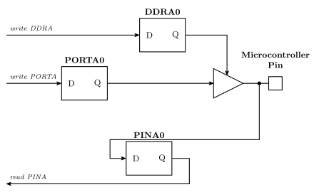
Figure 2: One bit of an AVR port — the three flip-flops behind pin PA0. DDRA0 enables the tri-state buffer, so it decides whether PORTA0’s value is driven onto the pin or the pin is left free for something outside to drive. PINA0 samples whatever is on the pin either way. Hence: DDR is direction, PORT is what you write, PIN is what you read.
1 means output, 0 means input. Writing 0xFF to DDRA makes every bit of port A an output, and writing 0x00 to DDRB makes every bit of port B an input.
Three consequences fall straight out of the circuit:
- PORTx does nothing on a pin whose DDRx bit is 0. The buffer is off; the value sits in the flip-flop unused. (On real AVR hardware it switches an internal pull-up instead.)
- PINx is always live. It samples the pin whether the pin is being driven from inside or outside, so reading PINx on an output pin reads back what you are driving.
- Reading PORTx is not reading the pin. It gives you the value you last wrote. To find out what is there, read PINx — which is why every input example uses
in rd, PINxand neverin rd, PORTx.
in and out
The two instructions that reach the first 64 I/O registers:
| Does | Operands | |
|---|---|---|
in rd, P |
Load I/O register value into general purpose register | rd: r0 to r31. P = I/O register number (0 to 63, 0x00 to 0x3F) or name |
out P, rr |
Store value from general purpose register into I/O register | rr: r0 to r31. P = 0 to 63 (0x00 to 0x3F) or name |
The operand order flips between them, and it flips for a consistent reason: like every AVR instruction, the destination is written first. So the I/O register is the second operand of in and the first of out.
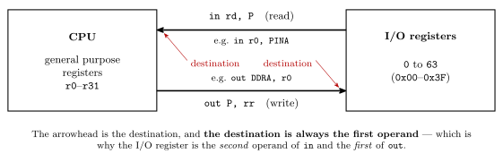
Figure 3: in and out between the two register files: the CPU’s general purpose registers r0–r31 and the first 64 I/O registers. in reads from an I/O register into a general purpose register, out writes the other way, and the head of each arrow, marked destination, is the operand written first. That is why the I/O register is the second operand of in and the first of out.
Answers of the form in DDRB, r16 are the standard trap. What is wrong with them is the mnemonic, not the direction: in’s destination is always one of r0–r31, so it can never be DDRB. Moving a general purpose register into an I/O register is exactly what out does — which is why the right answer in that shape is out DDRB, r16.
in and out reach all 32 general purpose registers, r0–r31 — unlike ldi, they are not restricted to the top half.
Both are one instruction word and one clock cycle, which makes them the cheapest way to touch a peripheral.
Three equivalences, all of them just the number/name table above:
| Written with a number | Same instruction, written with a name |
|---|---|
in r0, 0 |
in r0, PINA |
out 1, r0 |
out DDRA, r0 |
in r5, 0x26 |
in r5, TCNT0 — I/O register 0x26 is timer/counter 0 |
Using port names
Numbers are how the machine sees it; names are how you should write it:
.include "m324Adef.inc"The contents of this file are included directly in the program, and it defines the names for the I/O registers — so DDRA, PORTA, PINA, TCNT0 and the rest can be written instead of 0x01, 0x02, 0x00, 0x26. Everything about the generated machine code is identical; the assembler substitutes the number.
Setting port A (all bits) to be an output, which is the shape of nearly every initialisation block:
    ldi  r16, 0xFF       ; every bit 1 = output
    out  DDRA, r16       ; ... into the direction register
or, using the shorthand of avr-instructions, ser r16 in place of the ldi. Setting a port to be all inputs is the same two lines with 0x00 (or clr), and a mixed port is any other constant — DDRA is a bit pattern like everything else, so ldi r16, 0x0F gives four outputs and four inputs.
Changing one bit of a port
Writing a whole port register is right at initialisation. Afterwards a program usually wants to change one pin and leave the other seven alone, because the other pins belong to other parts of the program. In C that is a read-modify-write with a one-bit mask, the bit named rather than given as a number (bit-masking):
DDRC  |= (1<<5);          /* PC5 becomes an output     */
PORTC |= (1<<5);          /* PC5 driven high           */
PORTC &= ~(1<<5);         /* PC5 driven low            */
PORTC ^= (1<<5);          /* PC5 flipped               */
if (PINC & (1<<2)) { }    /* is PC2 high?              */
In assembly there are two ways:
| Register | Set or clear one bit | |
|---|---|---|
I/O registers 0 to 31, which includes every PINx, DDRx and PORTx |
sbi PORTC, 5 and cbi PORTC, 5 |
one instruction, other bits untouched |
any register in/out reach, 0 to 63 |
in r16, TCCR0B, then ori or andi with the mask, then out TCCR0B, r16 |
three instructions, and a spare register |
sbi and cbi hold the register number in five bits of the instruction, so they reach only the first 32 I/O registers. TCCR0B is I/O register 0x25, 37, which is past them: the long way is the only way. The extended registers past 63, such as TIMSK2 and TCCR1B, need lds and sts in place of in and out.
Writing to PINx
PINx is the port’s input register: reading it gives the levels on the pins. Writing to it is not storing a value. On the ATmega324A, writing a 1 to a bit of PINx toggles the matching bit of PORTx, whatever the pin’s direction, and writing a 0 does nothing.
That makes PINx a quick way to flip a pin:
PINC = (1<<0); /* toggle PC0; the 0s written to the other bits do nothing */and in assembly sbi PINC, 0 does the same in one instruction.
It also makes PINx the wrong register for a clear or a set. PINC &= ~(1<<5) does not clear PC5. If the compiler turns it into a single cbi PINC, 5, it writes a 0 to bit 5 of PINC and nothing happens. If it does a read, an AND and a write, it writes 1s to every other bit that read high, and those pins flip:
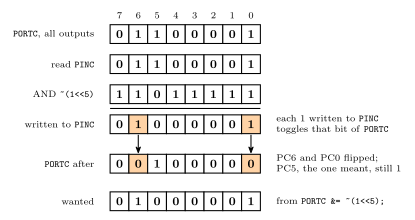
Figure 4: Why a read-modify-write on PINC goes wrong. Port C is all outputs, driving 0110 0001, so its pins read the same. PINC &= ~(1<<5) reads them, clears bit 5 of the reading and writes the result to PINC. A 1 written to a PINx bit is an order to toggle that bit of PORTx, not a value to keep, and a 0 does nothing. So the two other 1s, shaded, flip PC6 and PC0 low, and PC5, the bit meant to be cleared, stays high. The bottom row is what PORTC &= ~(1<<5) would have given.
So: set and clear through PORTx, read through PINx, and write PINx only to toggle.
Alternate pin functions
Most pins have a second job. When the peripheral that owns a pin is switched on, it takes the pin over from the port, and for some pins it overrides DDRx too. The serial interfaces use these:
| Port pin | Package pin | Alternate use | Peripheral |
|---|---|---|---|
| PB0 | 1 | XCK0 | USART0’s clock, used when it is an SPI master |
| PB4 | 5 | \(\overline{\text{SS}}\) | SPI (avr-spi) |
| PB5 | 6 | MOSI | SPI |
| PB6 | 7 | MISO | SPI |
| PB7 | 8 | SCK | SPI |
| PC0 | 22 | SCL | TWI |
| PC1 | 23 | SDA | TWI |
| PD0 | 14 | RXD0 | USART0 (avr-usart) |
| PD1 | 15 | TXD0 | USART0 |
| PD2 | 16 | RXD1 | USART1 |
| PD3 | 17 | TXD1 | USART1 |
| PD4 | 18 | XCK1 | USART1’s clock, used when it is an SPI master |
So the SPI port is the upper half of port B, and the TWI is the bottom two bits of port C. Other pins carry timer outputs, the external interrupts (INT0 and INT1 share PD2 and PD3 with USART1) and, on port A, the analog inputs. A pin can do only one job at a time, so a program that uses the SPI cannot also use PB4 to PB7 as general purpose I/O. The whole pinout is drawn in 2026-10-05-more-io.
Common mistakes
in DDRB, r16.inalways writes a general purpose register. Writing an I/O register isout DDRB, r16.- Reading
PORTxto find out what is on a pin. That gives back what was last written. The pins arePINx. - Setting or clearing a bit through
PINx. A 1 written there toggles, soPINC &= ~(1<<5)flips other pins and leaves PC5 alone. PORTC = (1<<5)to set one pin.=writes all eight bits and drives the other seven low. Use|=.sbiorcbion a register past 31, such asTCCR0B. They cannot reach it; usein,ori/andi,out.- Using a pin as general I/O while its peripheral is on. The SPI, the TWI and the USARTs take their pins over.
See also
- avr-architecture — the data address space these sit in, and the rest of the chip
- avr-instructions · avr-program-structure · bit-masking
- memory-models — why the I/O registers have two addresses
- io-board · device-pinouts — the switches, LEDs and buttons wired to the pins
- week6-lab-avr-io-ports — Lab 10, where this gets wired up
- avr-usart — PD0 and PD1 as a serial port · analog-to-digital-conversion — port A as analog inputs
- avr-spi — PB4 to PB7 as the SPI port · serial-communication — the TWI on PC0 and PC1
- 2026-08-31-instruction-set-architecture-part-1 — Lecture 11 · 2026-10-05-more-io — Lecture 19