Lab 10 — AVR Assembly and the AVR 324 Dev Board
Learning Lab 10, the first lab where a program leaves the simulator and drives real hardware. See avr-io-ports for the ports and registers, avr-program-structure for the template every task is built on, and io-board for the switches, LEDs and buttons being wired up.
What this lab covers
- AVR I/O ports: register numbers; port, pin and data direction registers;
INandOUTinstructions - Using and programming the 324 Dev board
- Assumed knowledge: Lectures 10 and 11, 2026-08-27-avr-introduction and 2026-08-31-instruction-set-architecture-part-1.
inandoutare Lecture 11 material that Lecture 12 repeats.
Admin — dongles. By the end of semester you will be using two USB-A cables for data (one for programming, one for serial communication), one of them from about halfway through the semester. On a personal laptop that may mean a dongle; there are workarounds, but they all have downsides. Get one sooner rather than later. (The same warning as in week5-lab-avr-assembly-one; this is the lab where the cable is first needed.)
From assembly program to chip
A very simplified description of what is happening inside the microcontroller in terms of low-level programming:
\[\text{assembly language program} \longrightarrow \text{machine code} \longrightarrow \text{ATmega324A}\]
The example program
    MOV R3, R5
    ADD R3, R4
    NEG R5
    IN  R3, PINA
    OUT R5, PORTB
assembles to 11010……, 11011……, … which is then downloaded into program memory (Flash — 32 kB). Inside the chip: program memory holding those words, data memory (SRAM — 2 kB), the AVR 8-bit CPU (ALU + CU + Reg), and other components.
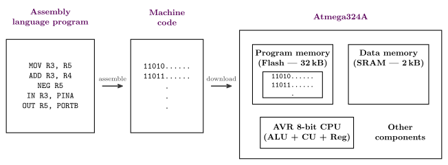
Figure 1: A very simplified picture of what is happening inside the microcontroller. Assembly text becomes machine code becomes the contents of flash; the CPU then reads it back out of flash one word at a time. The chip’s own panel is the point: program memory and data memory are separate blocks with separate address spaces (memory-models), which is why the machine code lands in one of them and the program’s variables in the other.
The last two lines of that program are the new part. Everything before them stays inside the CPU; IN and OUT are how a program reaches the outside world. Full picture in avr-architecture.
AVR I/O registers and general purpose I/O ports
- The ATmega324A has 224 I/O registers, accessible at memory addresses 32 (
0x20) to 255 (0xFF) with theld(load) andst(store) instructions. - The first 64 I/O registers (0 to 63) can also be accessed using
inandout. - Pages 636 to 639 of the datasheet (or the I/O register summary) have the I/O register details.
- Many registers are reserved (not used).
- The general purpose I/O port registers are
DDRA,PORTA,PINA,DDRB,PORTB,PINB, …
Extract from the I/O register list
The bottom of the list is the twelve port registers. The datasheet writes both numbers in one Address column: the I/O register number first, the data memory address in brackets after it.
Address — I/O reg no. (data memory address) |
Name |
|---|---|
0x0B (0x2B) |
PORTD |
0x0A (0x2A) |
DDRD |
0x09 (0x29) |
PIND |
0x08 (0x28) |
PORTC |
0x07 (0x27) |
DDRC |
0x06 (0x26) |
PINC |
0x05 (0x25) |
PORTB |
0x04 (0x24) |
DDRB |
0x03 (0x23) |
PINB |
0x02 (0x22) |
PORTA |
0x01 (0x21) |
DDRA |
0x00 (0x20) |
PINA |
I/O reg number (0–63) — used with
IN/OUT
Data memory address — used withLD/ST
Further up the same table are 0x15 (0x35) TIFR0 through 0x18 (0x38) TIFR3, with 0x14 (0x34) marked Reserved.
Each row also carries the eight bit names for that register — PORTD7 … PORTD0, DDD7 … DDD0, PIND7 … PIND0 — which is where the per-pin names come from. The data-direction bits are DDDn/DDCn/DDBn/DDAn, not DDRDn: the register is DDRD, its bits are DDD7–DDD0.
Two numbers for one register, differing by the 0x20 the general purpose register file occupies at the bottom of the data space. Which number you write depends on which instruction you use, and the two worked questions below both turn on getting that right. See avr-io-ports.
GPIO ports
The datasheet block diagram has PORT A (8), PORT B (8), PORT C (8) and PORT D (8) around the edges of the chip: four 8-bit ports, PA7..0, PB7..0, PD7..0 — and port C as PC5..0 with TOSC1/PC6 and TOSC2/PC7 broken out, since those two pins are shared with the timer oscillator (avr-io-ports).
PIN, PORT and DDR registers
One bit of one port is three D flip-flops, DDRA0, PORTA0 and PINA0, around a tri-state buffer and one microcontroller pin. DDRA0 enables the buffer, PORTA0 supplies what it drives, and PINA0 samples whatever is on the pin. Drawn out and read through in avr-io-ports.
in and out
in rd, P |
Load I/O register value into general purpose register | rd: r0 to r31; P = I/O register number (0 to 63, 0 to 0x3F) or name |
out P, rr |
Store value from general purpose register into I/O register | rr: r0 to r31; P = 0 to 63 (0 to 0x3F) or name |
The “or name” form is covered under Using port names below.
Worked: setting port A to all outputs
Which instructions will set all bits of port A to be outputs?
Answer:
    ldi r16, 0xFF
    out 0x01, r16
From the table above, I/O register 0x01 is DDRA, and a 1 in a direction bit means output, so 0xFF makes all eight pins outputs. Three wrong answers, each one lookup away:
| Changed line | Why not |
|---|---|
out 0x02, r16 |
0x02 is PORTA — this writes an output value, not a direction |
ldi r16, 0x00 |
right register, wrong value — 0x00 makes all eight pins inputs |
out 0x00, r16 |
0x00 is PINA — the read register |
Right and wrong answers are the same two instructions; only the constant and the I/O register number move.
Using port names
Including the m324Adef.inc file lets a program use names for I/O registers rather than numbers:
.include "m324Adef.inc"The contents of this file are included directly in the program. So the answer above can be written without ever looking up a number:
    ldi  r16, 0xFF       ; every direction bit 1 = output
    out  DDRA, r16
Identical machine code — the assembler substitutes 0x01 for DDRA. Write the names; look the numbers up only when reading someone else’s listing or an exam question.
Worked: setting port B to all inputs
Which instructions will set all bits of port B to be inputs?
Answer:
    ldi r16, 0x00
    out DDRB, r16
Two independent things have to be right:
out, notin.inloads from an I/O register into a general purpose one.in DDRB, r16is not a legal instruction at all:in’s destination is written first and must be one of r0–r31, andDDRBis not one of those.in r16, DDRBis legal — it reads the direction register into r16, throwing away the constant just loaded there, and changes nothing.0x00, not0xFF.out DDRB, r16with0xFFin r16 is the correct instruction with the value that makes every pin an output.
Across the two questions, the pair that must line up is (direction register, direction value): 1 is output and 0 is input.
ser and clr instructions
Short-hand ways of setting/clearing all bits of a register:
ser rd (set register) |
exactly the same as ldi rd, 0xFF — only works with registers ≥ 16 |
ser r16 |
clr rd (clear register) |
exactly the same as eor rd, rd |
clr r3 |
So both answers above can drop the constant — one instruction swapped for one, same two-line shape: ser r16 / out DDRA, r16 and clr r16 / out DDRB, r16. The asymmetry in which registers each reaches is not arbitrary — it follows from what they expand to; see avr-instructions.
Labels and the jmp instruction
        jmp RESET
        …
RESET:  …
        …

loop:   …
        …
        jmp loop
AVR assembly language program template
                             ; Comments start with semicolons
.include "m324Adef.inc"
    jmp RESET                ; <- vector table
    ; Interrupt handlers go here
    ; (more on this in week 9/10)

RESET:                       ; Starting point   <- RESET handler
    ...                      ; Initialisation code
                             ; e.g. set DDRs
loop:
    ...                      ; Do stuff        <- main code
    jmp loop                 ; Repeat
Three labelled sections — vector table, RESET handler, main code. Why it has that shape, and why the main body is an infinite loop, is in avr-program-structure.
Connecting the programmer
When attaching the programmer’s ribbon cable to the breadboard:
Red wire on the ground side
Getting this wrong damages hardware. See the Pololu Programmer Guide on Blackboard for the rest.
Tasks
Task 1 — AVR assembly program
Write an AVR program to
- read the value on port A pins
- flip (invert) all the bits
- write the value out to port C
- do this repeatedly
Remember to set data direction registers appropriately before reading/writing values.
Enter the code into Microchip Studio, simulate your code, check that it works by checking the appropriate registers.
Task 2 — Programming the AVR board
Connect 8 switches on the IO Board to AVR port A; and 8 LEDs to AVR port C.
- Use 4-way cables with 4-way headers on each end
- Build and download the program you wrote in task 1
See the Pololu Programmer Guide on Blackboard.
Test your program — change the values on the switches connected to port A and observe the LEDs.
Modify your program to output the two’s complement (negative) of the input, rather than the ones’ complement (inversion). Build, download and test it.
Task Three — Adding inputs
Connect 8 switches on the IO Board to AVR port A; and 8 LEDs to AVR port C; and connect the 4 push buttons on the IO Board to AVR port D (4 least significant bits).
- Use individual jumper wires for this if required
Write an AVR assembly language program to repeatedly
- Read the value on port A pins (8 bits)
- Read the value on port D pins (8 bits)
- Clear the upper nybble (4 bits) of this value (read from the four buttons); consider bitwise AND to do this
Add the two values and output the result to port C.
Make sure you set the data direction registers appropriately.
Build, download and test your program and verify it behaves as expected.
Task Four — Population count
- Count the number of high bits
- Read through
popcount.pdfon BlackBoard - Several variations (extension tasks)
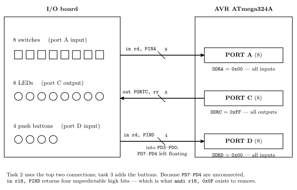
Figure 2: What tasks 2 and 3 ask you to wire, and what each port’s data direction register has to say about it. The direction rule is what fixes each DDR value: 1 is output, 0 is input. The four unconnected port-D pins are the reason task 3 asks for a bitwise AND.
Working — Task 1
The three things the task asks for map one-to-one onto three instructions, and the fourth (“do this repeatedly”) is the jmp at the bottom of the template.
.include "m324Adef.inc"

    jmp RESET

RESET:
    clr  r16
    out  DDRA, r16       ; port A: all inputs  (0 = input)
    ser  r16
    out  DDRC, r16       ; port C: all outputs (1 = output)

loop:
    in   r17, PINA       ; read what is actually on the pins
    com  r17             ; ones' complement - flip every bit
    out  PORTC, r17      ; drive the result out
    jmp  loop
Four things worth being deliberate about:
PINAfor the read,PORTCfor the write. ReadingPORTAwould give back whatever was last written to it, not what the switches are doing; writingPINCwould not drive anything. Input side reads PIN, output side writes PORT — see avr-io-ports.- The direction registers are set once, in
RESET, not inside the loop. They do not change. ser r16needs r16 or above, which is why the scratch register isr16rather than, say,r3.clrwould have been happy either way.comis the inversion the task asks for — ones’ complement, i.e. flip every bit (avr-instructions).
Simulating it, as the task asks: Microchip Studio’s simulator has no switches, so set PINA by hand in the I/O view and single-step; r17 should show the complement and PORTC should follow it.
Working — Task 2
Same program, now on real hardware: 8 switches → port A, 8 LEDs → port C, 4-way cables at both ends. Flip a switch and the corresponding LED should go off — the inversion is visible as switch and LED disagreeing on every bit.
The modification is a one-instruction change:
    in   r17, PINA
    neg  r17             ; two's complement instead of ones'
    out  PORTC, r17
com gives \(\overline{x}\); neg gives \(\overline{x} + 1\), which is the two’s complement negation (binary-number-representations). The two differ by exactly one, so on the LEDs the difference is a single increment — easiest to see with all switches down: com shows 1111 1111, neg shows 0000 0000.
Working — Task 3
Three ports now, and one masking step:
.include "m324Adef.inc"

    jmp RESET

RESET:
    clr  r16
    out  DDRA, r16       ; port A: 8 switches, all inputs
    out  DDRD, r16       ; port D: 4 buttons on the low nybble, all inputs
    ser  r16
    out  DDRC, r16       ; port C: 8 LEDs, all outputs

loop:
    in   r17, PINA       ; the eight switches
    in   r18, PIND       ; the four buttons - in the low nybble
    andi r18, 0x0F       ; clear the upper nybble
    add  r17, r18
    out  PORTC, r17      ; sum to the LEDs
    jmp  loop
Why the mask is needed at all, since only four pins are wired: in r18, PIND reads all eight bits of port D, and the four upper pins have nothing connected to them. An unconnected input pin floats, so those bits are unpredictable — masking them off is what makes the sum depend only on the buttons. andi r18, 0x0F is the extract case of bit-masking: 1s on the bits to keep, 0s on the bits to discard.
andi works here because r18 is a high register. Reading the buttons into a low register instead would need the mask in a register of its own:
    ldi  r19, 0x0F
    and  r5, r19
add r17, r18 writes into r17, since AVR is two-operand (avr-instructions) — so the switch value is consumed by the addition, which is fine, it is re-read at the top of every pass.
What to expect on the board: switches give 0–255, buttons add 0–15, and the sum is 8-bit, so pressing buttons with the switches near 0xFF wraps around. That wrap is the carry being discarded, and it is worth watching for deliberately — it is the same 8-bit-only arithmetic that the 16-bit addition in 2026-09-03-instruction-set-architecture-part-2 exists to work around.
Working — Task 4
popcount.pdf on Blackboard has both the method and the extension variations.
One approach with the instructions met so far: shift the value one bit at a time and count the bits that fall out into C. lsr moves bit 0 into the carry flag (avr-instructions), so eight shifts pass every bit through C in turn, and a conditional add of 1 to a counter each time gives the population count. It needs two things beyond those instructions: a carry-conditional branch and a loop counter.
See also
- avr-io-ports — the I/O registers, the three port registers, and
in/out - avr-program-structure — the template, labels and
jmp - avr-instructions · bit-masking · avr-architecture
- io-board — the switches, LEDs and buttons being wired to the ports
- week5-lab-avr-assembly-one — Lab 9, the simulator-only predecessor
- 2026-08-31-instruction-set-architecture-part-1 · 2026-09-03-instruction-set-architecture-part-2 — Lectures 11 and 12