Memory Models
The first of the four things that make up an ISA (instruction-set-architecture): how memory looks to the CPU. Four issues decide that — addressable cell size, alignment, address spaces and endianness — and every one of them is a decision the specification has to make, not something the hardware settles on its own.
Memory as addressable cells
Computer memory is conceptually a set of addressable cells:
- Each cell has a unique address (or cell number).
- Cells are usually 8 bits wide (i.e. hold one byte).
- Various cell widths have been used in the past — 8 bits is a convention, not a law.
Drawn as a table, the address indexes the rows and the cell width is how wide each row is:
| Address | ← cell width → |
|---|---|
| 0 | |
| 1 | |
| 2 | |
| 3 | |
| … |
A “4 × 3 memory” in that notation means 4 addresses of 3-bit cells — and \(4 = 2^2\), so two address bits. Built at gate level, it shows that “memory” at this level is nothing more exotic than flip-flops-and-latches and combinational-logic-blocks arranged into storage.
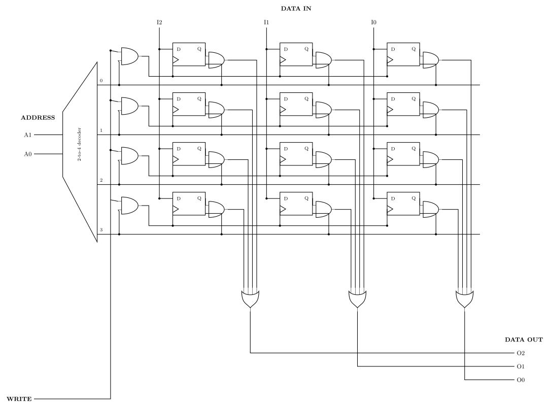
Figure 1: A 4 × 3 memory at gate level — four addresses of three-bit cells. Twelve D flip-flops in four rows of three: one row is one addressable cell. The decoder turns A1 A0 into exactly one row-select (word) line. Writing: the word line ANDed with WRITE clocks that row’s three flip-flops, so DATA IN (I2 I1 I0) — which is wired to every row’s D inputs all the time — is captured only by the selected row. Reading: each flip-flop’s Q is ANDed with its own word line and the three cells of a column are OR’d together, so the unselected rows contribute 0 and DATA OUT (O2 O1 O0) carries the selected row alone. The decoder is drawn as a trapezoid with the wide edge on the right, and the flip-flops as plain rectangles with a clock wedge on the lower-left edge, per this course’s conventions (csse2010-diagram-notation). The most significant bit, I2/O2, is the leftmost column.
A. Addressable cell size
Most common cell size is 8 bits (1 byte) — but not always.
The AVR is the counterexample sitting on the bench:
| AVR memory | Cell width |
|---|---|
| Data memory | 8 bits |
| Instruction (program) memory | 16 bits |
Which is why an AVR instruction is “one word” rather than “two bytes” — a program-memory address counts 16-bit cells.
The bus transports the content of a cell, but the data bus may be wider than one cell: it can retrieve several cells (addresses) at once. When it does, the address bus does not need to be as wide.
Bus sizes
For every doubling of the data bus width, remove the least significant bit of the address bus.
For a memory of \(2^n\) cells at 8 bits per cell — so an address size of \(n\) bits:
| Data bus | Address bus | Cells per transfer |
|---|---|---|
| 8 bits | \(n\) bits | one cell at a time |
| 16 bits | \(n-1\) bits | two cells at a time |
| 32 bits | \(n-2\) bits | four cells at a time |
The reason is that a wide transfer always moves an aligned group of cells. With a 16-bit data bus the memory only ever hands over cell pairs \((0,1), (2,3), (4,5), \dots\) — so the bottom address bit never selects anything, and naming the pair takes one bit fewer than naming the cell.
Worked example. A memory of 64 cells, 8 bits each, addressed 000000 … 111111:
\[64 = 2^6 \text{ cells} \implies 6\text{-bit addresses}\]
| Data bus | Address bus |
|---|---|
| 8 | 6 |
| 16 | 5 |
| 32 | 4 |
Read the two buses as a pair, not separately: widening one narrows the other by exactly as much.
Word addresses and byte addresses
The AVR’s 16-bit program-memory cells have one practical consequence. The program counter, jmp, call and every code label count words. But a table of constant bytes kept in flash is read a byte at a time by lpm, load program memory, and lpm takes a byte address in the Z register. Word \(w\) holds bytes \(2w\) and \(2w + 1\), with the low byte at the even address, which is the AVR being little endian (section D).
So turning a code label into a byte address means doubling it. Take the string Hello stored at word 2 by mesg: .db 72,101,108,108,111 (assembly-process):
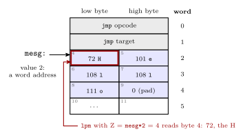
Figure 2: One region of program memory addressed two ways. Each row is a 16-bit word, numbered on the right, and each half is a byte, numbered inside its cell. The label mesg has the value 2 because labels in the code segment count words. Byte addressing counts the halves, low byte first, so word 2 starts at byte 4. That is why lpm is pointed at mesg*2: with Z = 4 it loads 72, the H. The five bytes of the string take two and a half words, and the last half word is a zero pad. Grey marks the jmp, blue the string and red the byte that lpm reads.
        ldi  ZH, high(mesg*2)   ; Z = 4: byte address of word 2
        ldi  ZL, low(mesg*2)
        lpm                     ; r0 <- 72, the H
Leaving out the *2 points Z at byte 2, the low byte of word 1, which is half of the jmp.
B. Alignment
Many architectures require natural alignment, e.g.
- 4-byte words starting at addresses 0, 4, 8, …
- 8-byte words starting at addresses 0, 8, 16, …
i.e. an \(n\)-byte value must start at an address that is a multiple of \(n\).
Taking an 8-byte word on a machine that fetches 8 bytes at a time:
| Where it sits | Reads needed | |
|---|---|---|
| Aligned | bytes 8–15, i.e. an 8-byte word at address 8 | 1 — it is exactly one fetched block |
| Non-aligned | bytes 12–19, i.e. an 8-byte word at address 12 | 2 — the top half of block 8–15, plus the bottom half of block 16–23 |
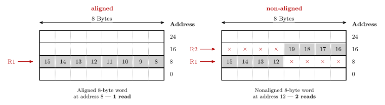
Figure 3: An aligned and a non-aligned 8-byte word. Four blocks of eight bytes; grey marks the bytes of the 8-byte word. On the left the word starts at address 8, so it is one block — one read. On the right it starts at address 12, so it takes the top half of the block at 8 and the bottom half of the block at 16 — two reads, marked R1 and R2. Two things about the drawing: addresses increase upward (unlike every other memory figure in the course, where they increase downward — see csse2010-diagram-notation on that inconsistency), and byte numbers within a row run high-to-low left to right. The × marks a byte in the fetched block that is not part of the word.
Alignment is often required because it is more efficient — the aligned case is always one read, the non-aligned case sometimes two, and the hardware that stitches two blocks together and extracts the middle is hardware that a machine demanding alignment simply does not need.
When alignment is not required — the Pentium IV
- Fetches 8 bytes at a time from memory (64-bit wide data bus).
- Alignment is NOT required, so the processor stays backwards compatible with earlier processors.
- A 4-byte word stored at address 4 takes 1 read (bytes 0 to 7).
- A 4-byte word stored at address 6 must read bytes 0 to 7 (one read) and bytes 8 to 15 (second read), then extract the 4 required bytes from the 16 bytes read.
Counting reads in general
A data bus \(w\) bytes wide delivers one aligned \(w\)-byte block per read. An \(n\)-byte value starting at address \(a\) therefore costs
\[\left\lceil \frac{(a \bmod w) + n}{w} \right\rceil \text{ reads}\]
The best case is \(n/w\) (rounded up), when the value starts on a block boundary; every other starting offset can push it one block further. So a value read from an arbitrary address costs either \(\lceil n/w \rceil\) or one more than that — which is why questions of this shape almost always answer “\(k\) or \(k+1\)” rather than a single number.
Worked example: an 8-byte value on a 16-bit data bus, no natural alignment required. Here \(w = 2\) and \(n = 8\):
| Starting address | Spans | Reads |
|---|---|---|
| Even | 4 aligned 2-byte blocks | 4 |
| Odd | 9 byte-positions, so 5 aligned blocks | 5 |
so the answer is 4 or 5. The odd case is the one to picture: one byte of the value sits alone at the top of the first block and one byte alone at the bottom of the last, and each of those still costs a whole read.
C. Address spaces
Many microprocessors have a single linear memory address space — the von Neumann architecture:
- e.g. \(2^{32}\) bytes numbered from 0 to \(2^{32} - 1\).
- (These may not be bytes — it depends on the addressable cell size.)
- Program and data share the one space.
However, the Harvard architecture has separate address spaces for instructions and data. The same numeric address means a different location depending on which space you are in, and an instruction says which one it means by what instruction it is.
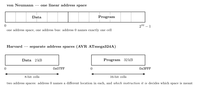
Figure 4: The two address-space models. Above: von Neumann — one linear space, so program and data are separated only by convention and address 0 names exactly one cell. Below: Harvard, in the AVR ATmega324A’s shape — two spaces, each starting at its own 0, with different sizes and different cell widths — and the cell width under each box is the whole reason the arithmetic below works out the way it does: 32 kB of program memory is \(2^{15}\) bytes but only \(2^{14}\) addresses, because each address there names a 16-bit cell. The end addresses follow from the sizes, so the data box ends at 0x07FF (\(2^{11}-1\), for 2048 bytes) rather than the 0x08FF of Figure 5, which is that 2 kB plus the 256 locations in front of it.
AVR ATmega324A is Harvard:
| Space | Size | Address width |
|---|---|---|
| Data | \(2^{11}\) (2048) bytes | 11 bits |
| Instruction | \(2^{14}\) 16-bit words — 16,384 instruction words = 32,768 bytes | 14 bits |
The arithmetic — convert to cells first, then take the logarithm:
\[\text{data: } 2\,\text{kB} = 2 \cdot 2^{10}\,\text{B} = 2^{11} \text{ cells (8-bit)} \implies 11 \text{ bits}\] \[\text{program: } 32\,\text{kB} = 2^{5} \cdot 2^{10}\,\text{B} = 2^{15}\,\text{B} = 2^{14} \text{ cells (16-bit)} \implies 14 \text{ bits}\]
The program-memory step is the one that catches people: 32 kB of flash is only \(2^{14}\) addresses, not \(2^{15}\), because each address names a 16-bit cell. Halve the byte count before taking the log whenever the cells are not bytes.
Laid out as a memory map (see avr-architecture for the rest of the chip):
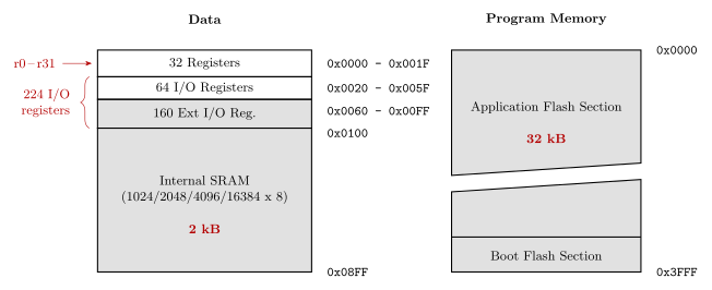
Figure 5: The ATmega324A’s two address spaces. Lowest address at the top, hex addresses outside on the right, grey fill on the coarsely-described regions, and the diagonal break across the flash meaning not to scale: that is this course’s memory-map convention (csse2010-diagram-notation). Marked in red: the register file is r0–r31, the 64 I/O plus 160 extended I/O registers are the 224 of avr-io-ports, the SRAM is 2 kB and the flash 32 kB.
Two details worth pinning down. 0x3FFF \(= 2^{14} - 1\), which is the 14 bits above. And the data space runs to 0x08FF — that is the 2 kB of SRAM plus the 256 locations (0x0000–0x00FF) that the register file and I/O registers occupy in front of it; the “\(2^{11}\) bytes” above is the SRAM itself, which is what the 11 bits size.
The assembler’s view: segments
An assembler treats each address space as a segment with its own location counter (assembly-process). On the ATmega324A there are three, because the EEPROM is a third address space alongside the two above:
| Segment | Directive | Address space | Cell | Counter starts at | The assembler can |
|---|---|---|---|---|---|
| code | .cseg |
program memory, flash, 32 kB | 16-bit word | 0x0000 |
place instructions and constants |
| data | .dseg |
data memory, SRAM | byte | 0x0100 |
only reserve space |
| EEPROM | .eseg |
EEPROM, 1 kB | byte | 0x0000 |
place constants |
Three consequences of separate spaces:
- The same number means different places. Address 0 is the reset
jmpin the code segment, registerr0in data memory and the first EEPROM byte in the EEPROM segment. - The units differ.
.org 0x0100in the code segment is word 256, which is bytes 512 and 513 of flash. In the data segment it is byte0x0100. - The data counter does not start at 0. The first 256 data addresses are the registers and I/O registers of Figure 5, so the first variable lands at
0x0100.
The data segment can only be reserved, not filled, because the assembler’s output is programmed into flash and EEPROM, which keep their contents, while SRAM starts empty at every power-up.
The memory behind each space
The three spaces are three different kinds of memory, and the kind explains how each is used (memory-technologies):
| Space | Technology | Volatile? | Erased and rewritten |
|---|---|---|---|
| Program memory | flash | no | electrically, a block at a time |
| Data memory | SRAM, flip-flops | yes | written a byte at a time, freely |
| EEPROM | EEPROM | no | electrically, one cell (byte) at a time |
The flash is divided into two blocks, the Application Flash Section and the Boot Flash Section of Figure 5. Because flash is erased a block at a time, a boot loader in the boot section can erase and rewrite the application section without erasing itself. Other AVR devices have one flash block, and some have more.
The register file and the SRAM sit at the top of the memory hierarchy. Unlike a desktop processor, the AVR has no cache: its SRAM is small enough and fast enough to keep up with the CPU directly.
D. Endianness
Different machines may support different byte orderings for a multi-byte value.
| Which end goes first (at the lowest address) | Used by | |
|---|---|---|
| Little endian | the little end — least significant byte | Intel microprocessors (Pentium etc.), and AVR |
| Big endian | the big end — most significant byte | SPARC, Freescale (formerly Motorola) microprocessors |
Most desktop/workstation/server CPUs produced since ~1992 are “bi-endian” (support both) — some switchable at boot time, others at run time, i.e. they can change dynamically.
Endianness only ever matters when a value spans more than one cell: reassembling it means knowing which cell was the low-order one.
Worked example
Given this memory:
| Address | Contents |
|---|---|
| 0 | 00001111 |
| 1 | 00110011 |
| 2 | 11011101 |
| 3 | 00101100 |
| Read | Value | Why |
|---|---|---|
| the 1-byte word at address 1 | 00110011 |
one cell — endianness does not apply |
| the 2-byte word at address 0, big endian | 00001111 00110011 |
big end first, so address 0 holds the most significant byte |
| the 2-byte word at address 2, little endian | 00101100 11011101 |
little end first, so address 2 holds the least significant byte and address 3 the most |
The mechanical way to do these without getting turned around: write the addresses the value occupies in increasing order, then assemble the answer most-significant-byte first. Big endian reads the addresses forwards; little endian reads them backwards.
See also
- instruction-set-architecture — the four pillars this is the first of
- avr-architecture — the ATmega324A’s two address spaces in full
- addressing-modes — how an instruction names a memory location
- binary-number-representations · flip-flops-and-latches · combinational-logic-blocks
- assembly-process — segments, location counters, and
.dbpacking two bytes to a word - compilation-and-linking — where a C compiler puts globals, locals and the heap in data memory
- memory-technologies — flash, SRAM and EEPROM as technologies, and why sizes are powers of 2
- memory-hierarchy-and-cache — registers, cache, main memory and disk, by speed and cost
- 2026-08-31-instruction-set-architecture-part-1 — Lecture 11 · 2026-10-08-assembly-process — Lecture 20 · 2026-10-22-memory-disks-and-files — Lecture 24