Memory Technologies
The kinds of memory a computer is built from, and how big they are. This note covers why a computer needs memory at all, the five ways memory is classified and where SRAM, DRAM, ROM, flash, SSDs and hard disks fall on each, how a static cell differs from a dynamic one, what “RAM” means now, the ROM family from ROM to flash, the ATmega324A’s three memories, the generations of DRAM, and the units capacity is quoted in, where “1 MB” can mean three different numbers. How these memories are arranged by speed is in memory-hierarchy-and-cache, and disks and files are in magnetic-disks and file-systems. First met in 2026-10-22-memory-disks-and-files.
Why a computer needs memory
A processor on its own holds a few dozen registers. Everything else has to live somewhere, and there are three distinct jobs:
- Temporary results. Intermediate values, variables, the stack: things a running program needs for a while and then discards.
- Programs. The instructions themselves have to be stored somewhere the processor can fetch them from (fetch-decode-execute-cycle).
- Settings that survive power-off. A calibration constant, a high score, the last channel a TV was on. These must still be there when the power comes back.
The first job wants memory that is fast and can be rewritten endlessly. The third wants memory that keeps its contents with no power. No single technology is best at all three, which is why there are many types.
Five ways to classify memory
Each axis asks one question about a memory.
| Axis | The question | The two answers |
|---|---|---|
| Access | Can any cell be reached directly, in the same time? | random access: the address selects the cell directly. Sequential access: the data has to be passed over in order to reach a cell, like a tape |
| Static or dynamic | Does a stored bit stay put by itself while powered? | static: held by a flip-flop or latch. Dynamic: held as charge that leaks away and must be refreshed |
| Volatility | Does it keep its contents when the power is off? | volatile: forgets. Non-volatile: remembers |
| Read-only | Can the processor write it in normal use? | read/write, or read-only (written once, or only by a special process) |
| Primary or secondary | Does the processor address it directly? | primary: on the processor’s address bus, holding the running program and its data. Secondary: reached through I/O, holding files |
Random access is what an address decoder gives you. In the gate-level memory of memory-models, the address bits drive a decoder that selects exactly one row, and it takes the same time whichever row it is. A tape has to wind past everything in front of the data first.
Where the common technologies fall:
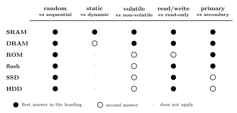
Figure 1: Six memory technologies against the five ways of classifying memory. Each row is one technology and each column one axis; a filled dot means the left-hand answer in the column heading, an open circle the right-hand one. SRAM and DRAM are both random-access, volatile, read/write primary memory, and differ only in being static or dynamic. ROM and flash are non-volatile; ROM is read-only, while flash is rewritten electrically, in blocks. SSDs (built from flash) and hard disks are secondary storage, reached through I/O rather than the address bus. All six are random access, in that any location can be reached directly by its address; the sequential case is tape. A hard disk’s access time does still depend on where the data is, because it must wait for the head to move and the disk to turn. The static/dynamic distinction only applies to the semiconductor RAMs, so it is left blank for the rest.
Two entries need a word. Flash is used both as primary memory (the program memory of a microcontroller like the AVR, which the processor fetches instructions from directly) and, packaged as an SSD, as secondary storage. And a hard disk counts as random access (sometimes called direct access) because the head can go straight to any track without reading what lies in between, unlike a tape. Reaching a sector still means moving the head and waiting for the sector to rotate underneath, though, so unlike a memory chip its access time depends on where the data is (magnetic-disks).
Static and dynamic memory
Static memory (SRAM) stores each bit in a flip-flop or latch: a loop of gates that holds its state for as long as the power is on (flip-flops-and-latches). Nothing needs doing to keep the bit. A typical cell is two cross-coupled inverters plus two switches to connect it to the bit lines, about six transistors per bit, so SRAM is fast but expensive per bit.
Dynamic memory (DRAM) stores each bit as charge on a capacitor, with a transistor as a switch that connects the capacitor to its bit line when the row is selected. One transistor and one capacitor per bit is far smaller than a flip-flop, so many more bits fit on a chip and each costs less. The price is that the charge leaks away. A DRAM cell forgets its contents within milliseconds unless it is refreshed, meaning read and written back, which the memory does to every row every few tens of milliseconds (of the order of 20 ms). Reading is slower too, because the small charge has to be sensed and amplified.
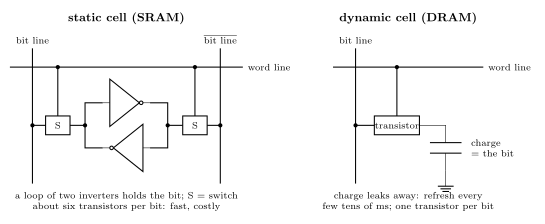
Figure 2: One bit of static and one bit of dynamic memory. Left: the static cell is two inverters in a loop. Whatever value sits at one side, the other inverter feeds its complement back, so the pair holds the bit for as long as there is power. Raising the word line closes both switches and connects the two sides to the bit line and its complement, for reading or writing. Right: the dynamic cell is a single switch (a transistor) and a capacitor. Raising the word line connects the capacitor to the bit line; a charged capacitor is a 1 and an empty one a 0. The charge leaks away through the switch, so the cell has to be read and rewritten, refreshed, every few tens of milliseconds.
| SRAM | DRAM | |
|---|---|---|
| Bit stored in | a flip-flop or latch | charge on a capacitor, behind a transistor switch |
| Keeps its bit while powered? | yes | only if refreshed every few tens of ms |
| Cell size | large (about six transistors) | small (one transistor, one capacitor) |
| Bits per chip | fewer | many more |
| Speed | faster | slower |
| Cost per bit | high | low |
| Volatile? | yes | yes |
| Typical use | registers, cache, small microcontroller RAM (the ATmega324A’s 2 kB) | a computer’s main memory |
What “RAM” means
RAM stands for random access memory. Originally that meant exactly the first axis above: any cell can be accessed directly, as opposed to sequential access. By that definition ROM and flash are random access too.
In current use “RAM” means volatile read/write memory, and SRAM and DRAM are the two kinds. So “RAM” and “ROM” are treated as opposites even though the original meaning of RAM covers both.
Volatile and non-volatile memory
Volatile memory forgets its contents when the power goes off. Both SRAM and DRAM are volatile. DRAM is volatile even with the power on, in the sense that it forgets within milliseconds if it is not refreshed.
Non-volatile memory remembers its contents with the power off. There are several kinds, and they differ in how, and how easily, they can be rewritten. Hard disks and optical disks are non-volatile too, but they are secondary storage; the next section is about non-volatile chips.
From ROM to flash
- ROM, read-only memory. The contents are hardwired into the silicon by the chip’s manufacturer. They can never be changed.
- EPROM, erasable programmable ROM. Programmed electrically by the user, and erased by ultraviolet light. An EPROM package has a small quartz window over the die. Shining a UV lamp through it for some minutes erases the whole chip, which can then be programmed again.
- EEPROM, electrically erasable PROM. Erased by applying a certain voltage, so it can be erased and rewritten in the circuit, with no lamp, one cell (byte) at a time.
- Flash. A newer form of EEPROM. The two used to be different technologies and have been converging. The main difference that remains is that flash is written and erased in blocks, where EEPROM is written and erased one cell at a time. Erasing a large block at once is what makes flash dense and cheap, and it is why flash holds programs and files while EEPROM holds a few bytes of settings that change one at a time.
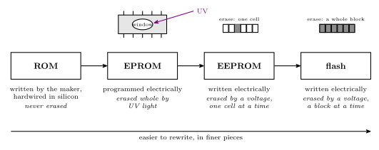
Figure 3: The family of non-volatile memory chips, from least to most easily rewritten. Each step keeps the contents with the power off and changes how they are erased. ROM cannot be erased at all: the bits are fixed when the chip is made. An EPROM is erased whole, by ultraviolet light shining through a window in the package. An EEPROM is erased electrically, in the circuit, a single cell at a time. Flash is erased electrically too, but a block of many cells at a time, which is what lets it be so dense.
The ATmega324A’s three memories
The ATmega324A has one of each of the three common kinds on the chip, and each is a separate address space with its own assembler segment (memory-models, assembly-process).
| Memory | Technology | Size | Holds | Volatile? | Assembler segment |
|---|---|---|---|---|---|
| Flash | flash (block-erased EEPROM) | 32 kB, as 16-bit words | the program and constant tables | no | .cseg |
| SRAM | static RAM | 2 kB | variables, the stack, the heap | yes | .dseg |
| EEPROM | EEPROM (cell-erased) | 1 kB | settings that must survive power-off | no | .eseg |
The flash is divided into two blocks: an application section, where the program normally lives, and a boot loader section at the top of program memory. A boot loader is a small program that can receive a new program, over a serial link for instance, and write it into the application section. Because flash is erased a block at a time, having the program in a separate block from the boot loader means the application can be erased and rewritten while the boot loader that is doing the rewriting stays intact. Other AVR devices have one flash block, and some have more.
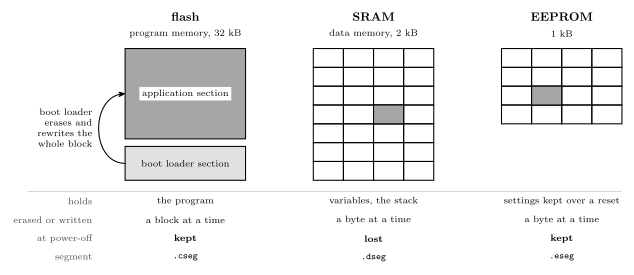
Figure 4: The ATmega324A’s three memories as technologies: what each holds, the unit it is erased or written in (dark), and whether it survives power-off. Flash holds the program and keeps it with the power off, but it can only be erased a block at a time, so it is split into two blocks: a boot loader in the small block can erase and rewrite the program in the large one without erasing itself. SRAM holds the variables and the stack; any byte can be written at any time, at full speed, but all of it is lost at power-off. EEPROM keeps its bytes with the power off and, unlike flash, erases and rewrites them one at a time, which suits a few settings that change one by one.
The table is the answer to a common question: which memory should this value go in? Code goes in flash. A variable the program changes goes in SRAM. A value the program changes and that must still be there after a reset goes in EEPROM.
Generations of DRAM
Every DRAM stores bits as charge on a capacitor, not in flip-flops. Its cells are smaller than a static cell, so a chip packs in more bits, and it is slower than static memory. What has changed over the generations is the interface, the way rows and columns are addressed and data is moved out:
| Generation | What it changed |
|---|---|
| FPM DRAM, fast page mode | once a row is open, further columns in that row can be read without re-sending the row |
| EDO DRAM, extended data out | keeps the output valid while the next column address is sent, so successive reads overlap; a refinement of FPM |
| SDRAM, synchronous DRAM | runs from a clock shared with the memory controller, so transfers happen on clock edges and can be pipelined |
| RDRAM, Rambus DRAM | a narrow, very fast proprietary bus |
| DDR SDRAM, double data rate, generations 1 to 5 | transfers data on both the rising and falling clock edges; each generation raises the rate |
| GDDR, graphics DDR, up to GDDR7 | a DDR variant tuned for the bandwidth of graphics cards |
FPM and EDO belong together as the asynchronous generations. SDRAM is the break: from there on, DRAM is clocked, and DDR4 and DDR5 are what current machines use.
Capacity units: powers of 2 or of 10
In SI units, kilo, mega and giga mean powers of 10: \(10^3\), \(10^6\), \(10^9\). In computing they have conventionally, or at least historically, meant the nearest powers of 2: \(2^{10} = 1024\), \(2^{20}\), \(2^{30}\). The two agree to within a few per cent, and the gap grows with every prefix.
| Prefix | Power of 10 | Power of 2 | Power of 2 is larger by |
|---|---|---|---|
| kilo (k) | \(10^3\) = 1,000 | \(2^{10}\) = 1,024 | 2.4 % |
| mega (M) | \(10^6\) = 1,000,000 | \(2^{20}\) = 1,048,576 | 4.86 % |
| giga (G) | \(10^9\) = 1,000,000,000 | \(2^{30}\) = 1,073,741,824 | 7.37 % |
| tera (T) | \(10^{12}\) | \(2^{40}\) = 1,099,511,627,776 | 9.95 % |
The percentages are measured against the power of 10: \((2^{30} - 10^9)/10^9 = 0.0737\).
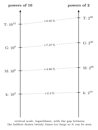
Figure 5: The decimal and binary meanings of each prefix side by side, on a log scale. Each step up the decimal ladder multiplies by 1000 and each step up the binary ladder by 1024, so the binary value pulls a little further ahead at every step: 2.4 per cent at kilo, 4.86 at mega, 7.37 at giga and almost 10 at tera. That is why the ambiguity is a rounding error for a kilobyte but a real difference for a terabyte disk.
Why main memory comes in powers of 2
A memory chip is addressed by address lines, and \(n\) lines can name exactly \(2^n\) cells: one line selects between 2 cells, two lines between 4, three between 8. A memory that used only 1,000,000 of the 1,048,576 addresses its 20 lines can name would waste the rest, so main memory is built in powers of 2 and its size is quoted that way: a “4 GB” module holds \(4 \times 2^{30}\) bytes.
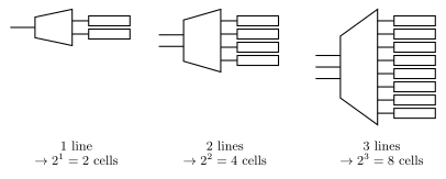
Figure 6: Why memory sizes are powers of 2. With one address line a decoder can select one of 2 cells, with two lines one of 4, and with three lines one of 8: every extra line doubles the number of cells that can be named. So n address lines give exactly 2 to the n cells, and a memory is built to fill that number.
Which convention is used where
| Context | Convention | Example |
|---|---|---|
| Main memory capacity | always powers of 2 | 1 GB \(= 1024 \times 1024 \times 1024\) B \(= 2^{30}\) B |
| Hard disk capacity, as sold | powers of 10 | 1 GB \(= 1000 \times 1000 \times 1000\) B \(= 10^9\) B |
| Operating systems (e.g. Windows) reporting sizes | powers of 2 | a “500 GB” disk shows as about 465.66 GB |
| Data speeds, transfer rates | usually powers of 10 | 1 Gbps (gigabit per second) \(= 10^9\) bits per second |
| Occasionally, a mixture | one of each | the 1.44 MB floppy disk: \(1.44 \times 1000 \times 1024\) bytes |
Disk makers’ powers of 10 make a disk seem bigger. A disk sold as 500 GB holds \(500 \times 10^9\) bytes, and an operating system that divides by \(2^{30}\) reports \(500 \times 10^9 / 2^{30} = 465.66\) “GB”. Nothing is missing; the two numbers use different gigabytes.
Note the case of the b: B is a byte and b is a bit. 1 Gbps is a rate in bits, so it moves \(10^9 / 8 = 125 \times 10^6\) bytes per second at most.
Binary prefixes: KiB, MiB, GiB
To avoid the confusion, standard names were created for the binary meanings:
| Name | Symbol | Value |
|---|---|---|
| kibibyte | KiB | 1024 bytes |
| mebibyte | MiB | 1024 KiB \(= 2^{20}\) bytes |
| gibibyte | GiB | 1024 MiB \(= 2^{30}\) bytes |
With these, kB, MB and GB can keep their SI meanings. Few people use them, though, and these notes use kilo, mega and giga as everyone does, with the meaning depending on the context. When the difference matters, say which one is meant.
Worked: what is a megabyte, and a gigabyte?
How many bytes is 1 MB? How many is 1 GB? How different are the meanings, and how many bytes does a “1.44 MB” floppy disk hold?
1 MB, three ways.
- Conventionally: \(1\text{ MB} = 2^{10}\text{ kB} = 1024\text{ kB} = 2^{20}\text{ B} = \mathbf{1{,}048{,}576}\) B.
- Sometimes, the SI meaning: \(1\text{ MB} = 10^6\text{ B} = \mathbf{1{,}000{,}000}\) B.
- Or in between, with a decimal mega of binary kilobytes: \(1000\text{ kB} = 1000 \times 1024 = \mathbf{1{,}024{,}000}\) B.
1 GB, three ways.
- Conventionally: \(1\text{ GB} = 2^{10}\text{ MB} = 2^{20}\text{ kB} = 2^{30}\text{ B} = \mathbf{1{,}073{,}741{,}824}\) B.
- Sometimes: \(1\text{ GB} = 10^9\text{ B} = \mathbf{1{,}000{,}000{,}000}\) B.
- Or in between: \(1000 \times 2^{20} = \mathbf{1{,}048{,}576{,}000}\) B, a thousand binary megabytes.
How different. The binary gigabyte exceeds the decimal one by \(1{,}073{,}741{,}824 - 1{,}000{,}000{,}000 = 73{,}741{,}824\) bytes, and
\[\frac{73{,}741{,}824}{1{,}000{,}000{,}000} = 0.0737 \approx 7.4\,\%.\]
That 7.4 % is measured against the decimal gigabyte. Measured against the binary one it is \(73{,}741{,}824 / 1{,}073{,}741{,}824 = 6.87\,\%\): the decimal gigabyte is 6.87 % smaller. For the megabyte the gap is \(48{,}576 / 1{,}000{,}000 = 4.86\,\%\). The in-between gigabyte, 1,048,576,000 B, is 4.86 % above \(10^9\) and 2.34 % below \(2^{30}\) (equivalently, \(2^{30}\) is 2.4 % above it).
The floppy disk. Its “1.44 MB” is 1.44 thousand binary kilobytes:
\[1.44 \times 1000 \times 1024 = \mathbf{1{,}474{,}560}\ \textbf{bytes} = 1440\text{ KiB}.\]
That is 1.40625 MiB in binary megabytes and 1.47456 MB in decimal ones. The label is right in neither, which is the point: it mixes a decimal thousand with a binary kilobyte.
Common mistakes
- Calling SRAM “dynamic” because it can be rewritten. Static and dynamic are about how a bit is held, a flip-flop against a leaking capacitor, not about whether it can change. Both are read/write.
- Thinking non-volatile means read-only. Flash and EEPROM are non-volatile and rewritable. ROM is the only one here that can never be rewritten.
- Thinking SRAM keeps its contents at power-off because it does not need refreshing. Static means no refresh while powered. Both SRAM and DRAM are volatile.
- Mixing up flash and EEPROM. Both are electrically erasable; flash erases a block at a time, EEPROM one cell at a time. On the AVR the program goes in flash and individual settings in EEPROM.
- Assuming “MB” has one meaning. Memory sizes are powers of 2, disk sizes and data rates are powers of 10, and some figures mix the two. Say which, or use KiB, MiB, GiB.
- Getting the 7.4 % backwards. \(2^{30}\) is 7.37 % more than \(10^9\), but \(10^9\) is 6.87 % less than \(2^{30}\). The base of a percentage matters.
- Confusing B and b. A 1 Gbps link is about 125 MB/s, not 1 GB/s.
See also
- memory-hierarchy-and-cache — how registers, cache, DRAM and disk are arranged by speed and cost
- magnetic-disks · file-systems — secondary storage and how files are kept on it
- memory-models — the ATmega324A’s address spaces and the three assembler segments
- avr-architecture — flash, SRAM and EEPROM on the chip
- flip-flops-and-latches — the storage element of a static memory cell
- assembly-process —
.cseg,.dsegand.eseg - 2026-10-22-memory-disks-and-files — Lecture 24