Lecture 10 — AVR Introduction
See instruction-set-architecture for machine instructions, the ISA and assembly language, avr-architecture for the chip, and avr-instructions for the instruction set and its encodings.
Outline
- Machine code
- Introduction to AVR — hardware, then assembly language
Recap
Basic computer organisation — ALU, control unit, registers, primary memory (cpu-organisation) — with the fetch-decode-execute cycle running over it: the instruction comes out of primary memory (F), is decoded (D), and is executed against the registers and ALU (E). Everything here is that picture made concrete on a real chip.
Machine code
Machine instructions
An example of Atmel AVR machine code: 0000 1101 0111 0111.
Instructions typically consist of:
- Opcode (operation code) — defines the operation, e.g. addition.
- Operands — what is being operated on, e.g. particular registers or a memory address.
So add rd, rr, meaning rd ← rd + rr, is an opcode (add) plus two register operands. (That example word decodes to a real instruction, worked out below.)
Instruction Set Architecture
An ISA is a specification — i.e. a document. It specifies the interface between hardware and software: software above the line is compiled without knowing how the chip works, hardware below it is built without knowing what will run. Drawn out in instruction-set-architecture.
Microarchitecture
Microarchitecture = the architecture of the control unit — i.e. the state machine (gates and flip-flops etc.) that implements the control unit.
Which is exactly the state-machines material from Lecture 8, now at processor scale.
An ISA can be implemented by many different microarchitectures. The 8086 ISA has been implemented by many processors in different ways; the Pentium ISA by Pentium, Pentium IV, Core2Duo and i7 (each differently), by various AMD devices, and by other manufacturers.
Assembly language
Machine code is too hard to program in, so we use assembly language: human readable (just!), and converted into machine code by software called an assembler.
add r3,r4 |
r3 ← r3 + r4 |
inc r22 |
r22 ← r22 + 1 |
The structural point: a high-level language compiles one-to-many, whereas assembly assembles 1:1 — one assembly instruction is exactly one machine instruction.
Introduction to Atmel AVR
Hardware
Atmel AVR devices are microcontrollers, which include lots of components on one chip: CPU, memory (RAM), program memory, input/output devices. A microprocessor is the CPU alone: an ATmega324A is not a CPU; it contains one, plus everything else needed to make a working system.
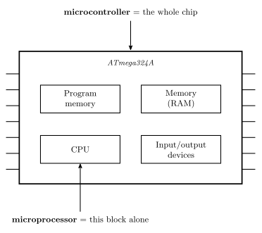
Figure 1: Microcontroller versus microprocessor. The four boxes are the four kinds of component, all in one package. The whole chip is the microcontroller, and only the CPU block is what would be sold on its own as a microprocessor. What a real ATmega324A actually contains is the chip diagram in the AVR architecture note.
On the AVR architecture diagram, the three regions of the cycle fall out of the block layout:
| Blocks | |
|---|---|
| F | Program Counter → Flash Program Memory → Instruction Register |
| D | Instruction Decoder → Control Lines |
| E | 32 × 8 general purpose registers → ALU → Status and Control |
Since those are separate hardware, they run concurrently on successive instructions — a three-stage pipeline. Drawn out, with the sizes and volatility of each memory, in avr-architecture.
Numbers worth having: program memory is 32 kB flash and non-volatile; the register file is 32 registers, R0–R31, each 8 bits wide and made of flip-flops; the ALU is 8-bit, which is what makes AVR an 8-bit machine; data SRAM is 2 kB and volatile; the data bus is 8 bits.
The peripherals on the ATmega324A datasheet block diagram fall into groups: the four 8-bit ports A–D are GPIO; USART 0, USART 1, SPI and TWI are communication; 8-bit T/C 0, 16-bit T/C 1 and 8-bit T/C 2 are the timers/counters; and the A/D converter and analog comparator go together as a fourth group. The 16-bit T/C 3 box is not in the timers/counters group: it belongs to the ATmega1284/1284P rather than the 324A. The three memories are FLASH for the program, SRAM for data, and EEPROM for non-volatile data. Those groupings are drawn out, with the package boundary and internal bus, in avr-architecture.
The AVR status register
8 bits, all R/W, all reset to 0:
| Bit | 7 | 6 | 5 | 4 | 3 | 2 | 1 | 0 |
|---|---|---|---|---|---|---|---|---|
| I | T | H | S | V | N | Z | C |
The five to know are the bottom five — S, V, N, Z, C. Four of them are the flags from Lecture 9 (fetch-decode-execute-cycle); I at bit 7 is the global interrupt enable.
AVR instructions
rd is the destination, rr the source. AVR is a two-operand machine — the destination is also an operand, so add rd, rr computes rd ← rd + rr. A three-operand ISA like ARM writes add rd, r1, r2 instead and leaves both sources alone.
| Instruction | Meaning | Example |
|---|---|---|
MOV rd, rr |
“move”, but actually copy: rd ← rr |
mov r3, r14 |
ADD rd, rr |
add rr to rd |
add r5, r6 → r5 ← r5 + r6 |
AND rd, rr |
bitwise AND into rd |
|
OR rd, rr |
bitwise OR into rd |
|
EOR rd, rr |
bitwise exclusive-OR into rd |
|
LDI rd, number |
load immediate — put the number into rd |
ldi r16, 73 |
LDI works for registers r16 to r31 only, with 8-bit numbers (00000000 to 11111111) — in decimal, the range \(-128\) to \(255\). ldi r0, 5 is not valid: r0 is below r16, so no such instruction exists. The reason is in the encoding, further down.
More instructions in coming weeks.
AVR machine code
Formats and bit-field diagrams in avr-instructions. Three encodings, each with a worked example:
ADD — 0000 11rd dddd rrrr
The 0000 11 is the opcode, bits 15–10; the remaining ten bits are the two five-bit register numbers, each torn into a single top bit and a low nibble. Watch the order in the middle: r (bit 9) comes before d (bit 8), the reverse of how the mnemonic writes them.
add r23, r7. The register numbers in binary, each split across its two fields:
- r23 \(= 16 + 4 + 2 + 1 = \texttt{10111}\), so
d= 1 anddddd=0111 - r7 \(= 4 + 2 + 1 = \texttt{00111}\), so
r= 0 andrrrr=0111
\[\texttt{0000 1101 0111 0111}\]
— which is the example word from the machine instructions section above. Drawn out field by field in avr-instructions.
COM — 1001 010d dddd 0000
Flip all bits (one’s complement). For com r19: r19 \(= 16 + 2 + 1 = \texttt{10011}\), so d = 1 and dddd = 0011:
\[\texttt{1001 0101 0011 0000}\]
LDI — 1110 KKKK dddd KKKK
K is the 8-bit constant, split into two nibbles either side of the register field, and d = register number − 16.
That subtraction is exactly why LDI is restricted to r16–r31: \(2^4 = 16\) — four bits of dddd can only name sixteen registers, and the ISA spends them on the upper half of the file.
Coming up
Instruction Set Architecture — more examples of AVR instructions.
See also
- instruction-set-architecture · avr-architecture · avr-instructions
- cpu-organisation · fetch-decode-execute-cycle · arithmetic-logic-unit · state-machines
- 2026-08-24-alu-and-control-unit — Lecture 9