Lecture 9 — From Digital Logic to Processors: ALU and Control Unit
The first half of the course, assembled into a processor. See cpu-organisation for the blocks, arithmetic-logic-unit for the ALU and its control table, and fetch-decode-execute-cycle for the control unit’s job. The worked examples, and the thread joining them, are below.
Where this sits
Everything so far has been gates, flip-flops and state machines. They assemble into the three blocks of a CPU: a control unit, an ALU, and registers, joined by internal buses and connected to memory and IO over external buses. Full picture in cpu-organisation.
The control unit fetches instructions from memory and makes the ALU and registers carry them out. There is enough of it below to see why the ALU needs the control inputs it has. The AVR used later in the course is an 8-bit machine with 32 general purpose registers, R0–R31, and therefore an 8-bit ALU.
Registers
Registers are temporary storage inside the CPU, in two kinds:
- General purpose registers — the data being operated on and the results. Collectively the register file; their width is the CPU word size.
- Special purpose registers — used by the system. Two of them: the Program Counter (PC), holding the address of the next instruction to be fetched, and the Instruction Register (IR), holding the current instruction.
Scale varies: a small CPU might have 8 × 8-bit registers, a large one 64 × 32-bit. Drawn out in cpu-organisation.
The ALU
The ALU is versatile hardware which can perform various operations based on some control inputs. A function/control input selects between addition, increment, subtraction, bitwise AND, bitwise OR and so on, so the ALU does considerably more than adding.
Its connections are of two kinds. A, B and Output are data (each an \(n\)-bit bus), while Function/Control is control (\(m\) bits). The ALU is one piece of hardware whose behaviour is chosen by wires coming from somewhere else.
Like adders, ALUs can be made up from 1-bit slices, and an \(n\)-bit ALU is \(n\) identical slices with the carry rippling through. The bit-slice circuit, the cascade and the full table of control combinations are all in arithmetic-logic-unit.
Two levels of control
The slice’s control inputs work at two different levels, and separating them is what makes the whole combinations table make sense:
- Permutations of the data inputs —
ENA,ENB,INVAcondition A and B before any function sees them. - Function select — \(F_1 F_0\) picks which operation’s result reaches the output:
| \(F_1 F_0\) | Function |
|---|---|
| 00 | A and B |
| 01 | invert B |
| 10 | A or B |
| 11 | A plus B |
The first three are logical, the last arithmetic.
What the conditioning gates do
Call the two conditioned lines \(X\) (on the A path) and \(Y\) (on the B path). Three gates produce them, and those three gates are the entire front end of the ALU:
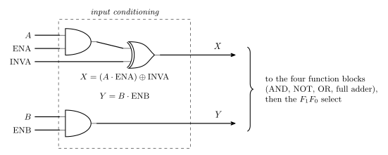
Figure 1: The input-conditioning gates of the bit slice. The two conditioned lines are X on the A path and Y on the B path. Nothing here selects an operation — these gates only decide what the four function blocks downstream get to see, which is why this is a separate level of control.
| ENA | INVA | \(X\) |
|---|---|---|
| 0 | 0 | \(0\) |
| 0 | 1 | \(1\) |
| 1 | 0 | \(A\) |
| 1 | 1 | \(\overline{A}\) |
| ENB | \(Y\) |
|---|---|
| 0 | \(0\) |
| 1 | \(B\) |
Being able to force an operand to a constant 0 or a constant 1 (all ones across the word, which is \(-1\) in two’s complement) is what lets a single ALU produce \(0\), \(1\), \(-1\), \(A+1\), \(B-1\) and \(-A\) with no dedicated hardware for any of them.
The same ALU without a multiplexer
The four-function ALU can be drawn in two forms. The simplified form routes the four results (\(A\) and \(B\), \(\overline{B}\), \(A\) or \(B\), and the adder’s sum) into a multiplexer whose select is \(F_1F_0\) (arithmetic-logic-unit). The full internal diagram, from Tanenbaum’s Structured Computer Organization, has no multiplexer at all: it feeds \(F_1F_0\) into a decoder, and the decoder’s four outputs are enable lines, one per function.
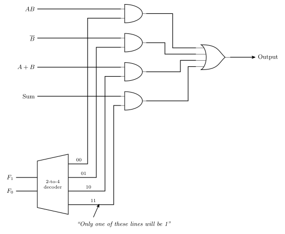
Figure 2: Selecting a function with enable lines instead of a multiplexer: a decoder turns F1 F0 into four enable lines, each function’s result is ANDed with its own enable line, and the four gated results are OR’d together. Because a decoder raises exactly one output, three of the AND gates emit 0 and the OR simply passes the fourth through. The decoder block stands for inverters plus four AND gates. The logical results are labelled AB, B-bar and A+B, but the gates actually see the conditioned X and Y of the previous figure. The enable-to-function mapping is the F1 F0 table above.
Only one of the enable lines is 1 at a time. That is the defining property of a decoder (combinational-logic-blocks), and it is what makes the final OR gate safe: three of its four inputs are guaranteed to be 0, so the OR is not combining anything, just passing the selected result through. The two drawings are therefore the same machine. A multiplexer is a decoder driving enable gates into an OR, which is exactly how the mux of combinational-logic-blocks is built inside.
Two other things the full diagram makes visible that the simplified one hides:
- the three logical functions form a logical unit and the adder is a separate full adder, so the slice is some logic, one adder, and a chooser;
- the carry-in to the adder is Carryin (INC), which is where the
INCcontrol input of the combinations table physically enters.
Example — calculating \(B - A\) using this ALU
The question is which values of \(F_1\), \(F_0\), ENA, ENB, INVA and INC make the ALU output \(B - A\).
Via two’s complement negation:
\[B - A = B + (-A) = B + (\overline{A} + 1) = B + \overline{A} + 1\]
\[\boxed{F_1 = 1 \quad F_0 = 1 \quad \text{ENA} = 1 \quad \text{INVA} = 1 \quad \text{ENB} = 1 \quad \text{INC} = 1}\]
Select the adder (\(F_1F_0 = 11\)), let \(A\) through and invert it (\(\text{ENA} = \text{INVA} = 1\), giving \(X = \overline{A}\)), let \(B\) through (\(\text{ENB} = 1\)), and set the carry into the bottom slice (\(\text{INC} = 1\)). Written as a column addition across the word for \(n = 8\):
\[\begin{array}{cccccc} & B_7 & B_6 & \cdots & B_1 & B_0 \\ + & \overline{A_7} & \overline{A_6} & \cdots & \overline{A_1} & \overline{A_0} \\ + & 0 & 0 & \cdots & 0 & 1 \end{array}\]
The bottom row is INC entering the least significant slice — so the \(+1\) of the negation costs no extra hardware at all.
Useful combinations
The full table of useful combinations of ALU inputs is in arithmetic-logic-unit. Three of its rows, worked through:
- \(B - 1\) — control input by control input: \(F_1F_0 = 11\) (adder), \(\text{ENA} = 0\) with \(\text{INVA} = 1\) so \(X\) is all ones, \(\text{ENB} = 1\) so \(Y = B\), \(\text{INC} = 0\). Across the word that is \(B_7 B_6 \dots B_0\) plus \(1\,1\,\dots\,1\), i.e. \(B + (-1)\).
- \(-1\) — the pattern \(11\dots1\). Here the same all-ones \(X\) is combined by OR with \(Y\) forced to zero, so the all-ones pattern passes straight through to the output.
- \(B + 1\) — by the same reasoning it is \(F_1F_0 = 11\), \(\text{ENA} = 0\), \(\text{ENB} = 1\), \(\text{INVA} = 0\), \(\text{INC} = 1\): force \(X\) to zero, pass \(B\), and add the carry.
The control unit
Fetch-decode-execute
The control unit operates in a continuous cycle on the datapath — fetch an instruction from memory into the CPU (PC and IR are the registers involved), decode it to resolve the opcode and operands, then execute, issuing control signals so the operation happens in the datapath. Written out as five steps, with the PC advancing before execution, and drawn as a loop, in fetch-decode-execute-cycle. The cycle is a three-stage pipeline.
Control signals
The datapath is a register file feeding two buses into the ALU, with the result returning on a destination bus. Controlling it means deciding four things:
- what the ALU does;
- which register values are placed on the A and B buses;
- which register receives the result from the destination bus;
- when to read or write memory.
Each is decided by a bundle of wires leaving the control unit, and their widths follow from the hardware they drive:
| Signal | Width | Why that width |
|---|---|---|
| A register select | 3 | \(2^3 = 8\) registers in the file (r0–r7) |
| B register select | 3 | same |
| Destination select | 3 | same |
| ALU control | 6 | the six ALU control inputs — \(F_1\), \(F_0\), ENA, INVA, ENB, INC |
| Memory read/write | 1 | one bit chooses the direction |
plus address and data lines to memory, and — coming back the other way — the ALU status lines feeding into the control unit. The whole figure is in fetch-decode-execute-cycle.
So r5 = r0 + r2 becomes: A select 0, B select 2, destination select 5, ALU control set to the \(A+B\) row of the combinations table.
Control signals come from the control unit, which must generate them in the right order for a given instruction — and the instruction is determined by the contents of the Instruction Register.
Data influencing control
The IR alone is not enough: the control unit can’t operate without knowing something about the data. If a for-loop variable is meant to run from 10 down to 0, the control unit has to know when it gets there.
That is what the status register is for. It is determined by ALU operations, stores the status of the last ALU operation, and is available to the control unit. if (x < 0) becomes, at this level, an ALU operation followed by the control unit reading a status bit.
ALU status flags
| Flag | Question |
|---|---|
| Z | zero bit — was the last result 0? |
| V | overflow bit — did the last addition/subtraction overflow, assuming a two’s complement operation? |
| C | carry bit — was a carry out generated? |
| N | negative bit — was the result negative as two’s complement, i.e. what is the sign bit? |
Typically held in a special purpose STATUS register (SREG) available to the control unit. The register is wider than four bits, and these four flags occupy its right-hand end.
Example — the flags after \(8_{10} - 9_{10}\) on a 5-bit ALU
First negate 9 in 5 bits: \(9 = 01001\), invert to \(10110\), add one to get \(10111\). Then add, keeping the carries into and out of the sign column:
\[\begin{array}{crl} \text{carry into MSB} \rightarrow & 0\phantom{0000} & \\ & 01000 & \\ + & 10111 & \\ \hline \text{carry out} = 0 \rightarrow & 11111 & \end{array}\]
\[Z = 0 \qquad C = 0 \qquad V = 0 \qquad N = 1\]
- \(Z = 0\) — the result is not zero.
- \(C = 0\) — nothing carried out of the top bit.
- \(V = 0\) — the carry into the sign column and the carry out of it are both 0, so they agree; equivalently, \(8 + (-9) = -1\) is well within 5-bit two’s complement range. See 2026-08-04-binary-arithmetic for the \(C_{in} \oplus C_{out}\) rule.
- \(N = 1\) — the sign bit is set.
And \(11111\) read as two’s complement is \(-1\), which is indeed \(8 - 9\).
See also
- cpu-organisation · arithmetic-logic-unit · fetch-decode-execute-cycle
- binary-number-representations — two’s complement, which the whole subtraction story rests on
- 2026-08-04-binary-arithmetic — the overflow rules the V flag implements
- combinational-logic-blocks — the decoder and multiplexer the function select is built from
- state-machines · logic-gates
- 2026-08-20-state-machines — Lecture 8