AVR Timers and Counters
The ATmega324A’s three timer/counter units: what they are, which pins and registers belong to each, how their clock is chosen and prescaled, the modes that decide what the count does when it reaches its top, the output compare actions that let a match drive a pin, and the one formula that turns a wanted event frequency into register values. From 2026-09-14-flow-of-control and 2026-09-17-pulse-width-modulation, with the register-level detail from week8-lab-avr-timers. PWM, the timers’ main use, has its own note: pulse-width-modulation.
Timer, counter
- A counter is a binary up/down counter clocked on some event.
- A timer is a counter clocked by a regular clock.
One piece of hardware, two names for what its clock is. Clock it from an external pin and each count is an event; clock it from the system clock and each count is a fixed slice of time, so the count is elapsed time. It is the wide, fast, silicon version of the counters of counters, and it is separate hardware from the CPU: once configured it counts, compares and drives its pins with no instructions running, which is the whole reason to have it.
Three things a timer/counter is used for, in this course:
| Use | Clock | The event |
|---|---|---|
| Timing — do something every 100 ms, toggle an LED, tick a clock | system clock ÷ prescaler | the count reaching a compare value or wrapping, at a known interval |
| Counting — how many pulses arrived on a pin | edges on the external pin Tn |
the count reaching a compare value: that many pulses |
| PWM — an adjustable-width pulse on a pin, in hardware | system clock ÷ prescaler | the compare match switching the OCnx pin partway through each sweep |
The three units
| Timer/Counter 0 | Timer/Counter 1 | Timer/Counter 2 | |
|---|---|---|---|
| Width | 8-bit (0–255) | 16-bit (0–65535) | 8-bit (0–255) |
| Output compare pins | PB3 = OC0A, PB4 = OC0B |
PD5 = OC1A, PD4 = OC1B |
PD7 = OC2A, PD6 = OC2B |
| External clock pin | PB0 = T0 |
PB1 = T1 |
none — TOSC1/TOSC2 (PC6/PC7) take a separate crystal instead |
| Prescaler taps | 1, 8, 64, 256, 1024 | 1, 8, 64, 256, 1024 | 1, 8, 32, 64, 128, 256, 1024 |
| Modes | Normal, CTC, Fast PWM, Phase Correct PWM | Normal, CTC, Fast PWM, PC PWM, PFC PWM | Normal, CTC, Fast PWM, Phase Correct PWM |
| Count register | TCNT0 |
TCNT1H:TCNT1L |
TCNT2 |
| Control registers | TCCR0A, TCCR0B |
TCCR1A, TCCR1B, TCCR1C |
TCCR2A, TCCR2B |
| Compare registers | OCR0A, OCR0B |
OCR1AH:OCR1AL, OCR1BH:OCR1BL |
OCR2A, OCR2B |
| Interrupt registers | TIMSK0, TIFR0 |
TIMSK1, TIFR1 |
TIMSK2, TIFR2 |
Every unit has two compare units, A and B, each with its own register and its own pin. Timer 1 is the one to reach for when 255 is not enough: its 16 bits give periods 256 times longer at the same prescaler, and it is the timer Lab 12 sets up. Timer 2 is the one with a separate clock source, for real-time-clock use. The T/C 3 in the family datasheet’s block diagram is on the ATmega1284, not this chip (avr-architecture).
The pins are shared with GPIO. OC0A is PB3 until timer 0 is told to drive it; configuring a compare output takes the pin away from PORTB and hands it to the timer. The DDR bit must still be set to output, since the timer only decides what the pin shows, not whether it drives.
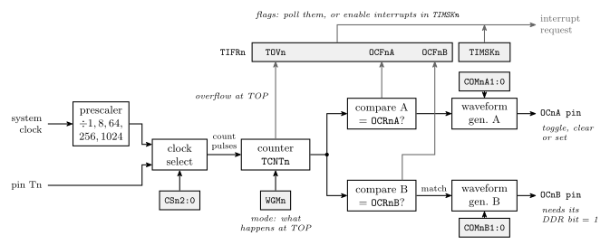
Figure 1: One timer/counter unit, from clock to pins. The clock select multiplexer feeds the counter either a prescaler tap or an edge on the external pin, or nothing; the counter increments on each pulse of whatever it is given. Two compare registers are each checked against the count every tick, and a match raises that unit’s flag and fires the waveform generator for its pin. Reaching the top of the count raises the overflow flag and, depending on the mode, wraps the count. The flags collect in TIFRn, where a program can poll them or, with the matching bits set in TIMSKn, have them raise an interrupt. Every box is configured through I/O registers and then runs with no CPU involvement.
Registers: data, control, interrupt
A timer is configured the way a port is — through I/O registers (avr-io-ports) — and its registers sort into the same three kinds:
| Timer registers | Port equivalent | ||
|---|---|---|---|
| data | TCNTn — the current count |
PIN / PORT |
read it to see where the count is; write it to preset |
| control | TCCRnA, TCCRnB (TCCR1C) — mode, clock, pin action; OCRnA, OCRnB — the values to match |
DDR |
set once, then leave |
| interrupt | TIMSKn — which events raise an interrupt; TIFRn — which events have happened |
— | read the flags by polling, or enable interrupts: avr-interrupts |
Where they are
The timer registers are spread across both the in/out range and the extended I/O space that only lds/sts reach (avr-io-ports):
| Register | I/O address | Data-memory address |
|---|---|---|
TCNT0 |
0x26 |
0x46 |
TCNT1L / TCNT1H |
— | 0x84 / 0x85 |
TCNT2 |
— | 0xB2 |
In C none of this matters: avr/io.h defines every one of them as a memory-mapped byte (c-preprocessor-and-avr-headers), and TCNT0, OCR1A and TCCR2B are assigned to like variables.
16-bit registers
Timer 1’s count and compare registers are two bytes each, and the hardware guards them with a shared temporary register so that a 16-bit value is read or written atomically: write the high byte first, then the low; read the low byte first, then the high. In assembly:
    ldi  r16, high(4321)
    sts  OCR1BH, r16       ; high byte first — goes into the temp register
    ldi  r16, low(4321)
    sts  OCR1BL, r16       ; low byte — both bytes land together
In C the compiler knows the rule, and OCR1B = 4321; is the whole thing. The H/L names still exist, but OCR1A, OCR1B, TCNT1 and ICR1 are 16-bit variables in the header.
The read rule has a consequence: reading TCNT1H on its own gives a stale value. Reading the low byte is what copies the high byte into the temporary register, and a read of the high byte returns that copy. So for the top half of the count, read the whole of TCNT1 and shift, as in TCNT1 >> 8, which reads the low byte first (below).
Choosing the clock
The count advances once per rising edge of whatever the clock select field CSn2:0 in TCCRnB picks — drawn as a multiplexer in 2026-09-14-flow-of-control:
CSn2 |
CSn1 |
CSn0 |
Timers 0 and 1 | Timer 2 |
|---|---|---|---|---|
| 0 | 0 | 0 | no clock — timer stopped | no clock |
| 0 | 0 | 1 | clk / 1 (no prescaling) | clk / 1 |
| 0 | 1 | 0 | clk / 8 | clk / 8 |
| 0 | 1 | 1 | clk / 64 | clk / 32 |
| 1 | 0 | 0 | clk / 256 | clk / 64 |
| 1 | 0 | 1 | clk / 1024 | clk / 128 |
| 1 | 1 | 0 | external pin Tn, falling edge |
clk / 256 |
| 1 | 1 | 1 | external pin Tn, rising edge |
clk / 1024 |
Two things to read off the table. A timer with CS = 000 does not run, which is both the reset state and the way to stop one. And timer 2’s codes are different — it spends the two external-pin codes on its extra prescaler taps — so a CS value copied from a timer-1 example means something else on timer 2.
The prescaler is a chain of dividers on the system clock (8 MHz on the lab boards), and each tap makes every count last that many system cycles. With an 8-bit timer the full 0-to-255 sweep therefore takes \(256 \cdot N\) cycles:
| Prescaler \(N\) | Tick | Sweep of 256 counts (8 MHz) | Sweep of 65536 counts (timer 1) |
|---|---|---|---|
| 1 | 0.125 µs | 32 µs | 8.2 ms |
| 8 | 1 µs | 256 µs | 65.5 ms |
| 64 | 8 µs | 2.05 ms | 524 ms |
| 256 | 32 µs | 8.19 ms | 2.1 s |
| 1024 | 128 µs | 32.8 ms | 8.4 s |
Coarse control over the period comes from this table; fine control comes from the compare registers and the mode.
Worked: a slow count from TCNT1 >> 8
With the clock divided by 1024, how quickly does TCNT1 >> 8 go up?
Timer 1 then counts \(8\ \text{MHz} / 1024 = 7812.5\) times a second. Shifting right by 8 drops the bottom eight bits, so what is left goes up by one every \(2^8 = 256\) counts:
\[\frac{7812.5}{256} = 30.5\ \text{Hz}, \quad\text{once every } 32.8\ \text{ms}.\]
TCNT1 >> 8 is the high byte of the count. It runs from 0 to 255 and comes back round to 0 every \(65\,536 / 7812.5 = 8.4\) seconds.
The same reasoning works for any shift. Each bit of a counter changes half as often as the bit below it, so TCNT1 >> k goes up \(7812.5 / 2^k\) times a second: 3906 for a shift of 1, 1953 for 2, and so on down to 30.5 for 8. A single bit is a square wave: (TCNT1 >> 12) & 1 changes every \(2^{12} = 4096\) counts, 0.52 s, which is enough to blink something about once a second without a single interrupt.
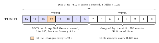
Figure 2: Timer 1’s count as a set of slower counters. With the clock divided by 1024 the whole of TCNT1 goes up 7812.5 times a second. Each bit changes half as often as the one to its right, so bit 8 changes once every 256 counts, and the top byte, TCNT1 >> 8, is a counter of its own that goes up 30.5 times a second and wraps every 8.4 s. Bit 12, shaded, changes every 0.52 s on its own.
In code, the timer only needs its prescaler, and it runs freely in normal mode:
TCCR1A = 0;
TCCR1B = (1<<CS12) | (1<<CS10);              /* normal mode, clock / 1024 */

uint8_t start = TCNT1 >> 8;
while ((uint8_t)((TCNT1 >> 8) - start) < 61) { }   /* 61 x 32.8 ms = 2.0 s */
The subtraction is done in 8 bits on purpose. When the count wraps from 255 to 0, now - start still comes out as the number of steps in between, so long as fewer than 256 have passed. week10-lab-adc-and-spi paces all its programs this way.
Modes: what happens at TOP
The waveform generation mode bits — WGM02:0 for the 8-bit timers, WGM13:0 for timer 1, split across TCCRnA and TCCRnB — decide what the count does when it reaches its TOP, and what TOP is:
| Mode | TOP | At TOP | Timer 0 WGM02:0 |
Timer 1 WGM13:0 |
|---|---|---|---|---|
| Normal | 0xFF / 0xFFFF | wrap to 0, set TOVn |
000 (0) |
0000 (0) |
| CTC — clear timer on compare match | OCRnA |
clear to 0, set OCFnA |
010 (2) |
0100 (4) |
| Fast PWM, fixed top | 0xFF | wrap to 0 | 011 (3) |
0101–0111 (8-, 9-, 10-bit) |
| Fast PWM, top in a register | OCRnA |
wrap to 0 | 111 (7) |
1111 (15; 1110 uses ICR1) |
| Phase correct PWM | 0xFF or OCRnA |
count back down | 001 (1), 101 (5) |
0001–0011, 1011 |
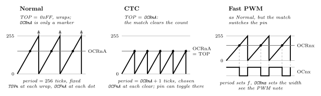
Figure 3: The three modes this course uses, as the count against time. In normal mode the counter runs to its full range and wraps; a compare value is just a marker it passes on the way, and the period is fixed at \(2^{8}\) or \(2^{16}\) ticks. In CTC mode reaching OCRnA clears the counter, so the compare value is the period and can be set to anything — the mode for producing an event at a chosen rate. In fast PWM the counter runs as in normal mode (or, in the register-top variant, as in CTC) while the compare match switches a pin partway through each sweep: the period sets the frequency and the compare value sets the pulse width. The same counter and the same compare registers produce all three; the mode bits only change what the top of the count means.
Normal is the mode after reset and the mode for a free-running count: read TCNTn to see how much time has passed, or let it overflow and take the overflow as the tick. CTC is the mode for an event every \(X\) ticks: the period is OCRnA + 1 exactly, with no wasted counts, and the count never exceeds the compare value. Both PWM modes are in pulse-width-modulation.
Output compare: what a match does to the pin
Each compare unit has two compare output mode bits, COMnx1:0 in TCCRnA, that decide what happens to the OCnx pin when TCNTn equals OCRnx. In the non-PWM modes (Normal, CTC):
COMnx1 |
COMnx0 |
On compare match |
|---|---|---|
| 0 | 0 | normal port operation — the pin belongs to the port, timer disconnected |
| 0 | 1 | toggle OCnx |
| 1 | 0 | clear OCnx — set the output low |
| 1 | 1 | set OCnx — set the output high |
Toggle is the useful one for a square wave: a CTC count that toggles the pin on every match produces a waveform whose frequency is half the match frequency, since it takes two matches for one full cycle. In the PWM modes the same bits select non-inverting (10) or inverting (11) output, and 01 becomes toggle OCnA on match only in the register-top mode — see pulse-width-modulation.
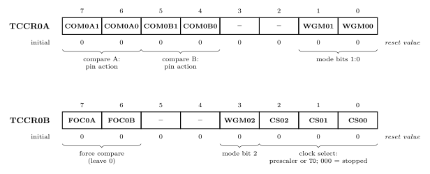
Figure 4: The two control registers of timer/counter 0, bit by bit, in the datasheet’s three-row form. The compare output mode fields sit at the top of TCCR0A, one two-bit field per compare unit; the three waveform generation mode bits are split, two at the bottom of TCCR0A and one in the middle of TCCR0B; the clock select field is the bottom three bits of TCCR0B. The two force-output-compare bits are for tests and are left alone. Every bit resets to 0, which decodes as normal mode, pins disconnected, timer stopped — so a timer does nothing until a program writes both registers. Timer 2’s registers have the same layout; timer 1 spreads the same fields over three registers with a fourth WGM bit.
Setting them from C uses the bit names from the header as shift counts, the idiom of bit-masking: TCCR1B = (1<<WGM12) | (1<<CS11) | (1<<CS10); selects CTC mode with clock ÷ 64 on timer 1, and TCCR0A = (1<<COM0A0); makes OC0A toggle on match. Write the whole register rather than |= when setting a timer up, so that nothing left over from before survives.
The master formula
Every timing question reduces to one relation between the clock, the prescaler and the top of the count:
\[f_{event} = \frac{f_{clk\_I/O}}{N \cdot (TOP + 1)}\]
- \(f_{clk\_I/O}\) is the device clock — 8 MHz on the ATmega324A boards.
- \(N\) is the prescaler: 1, 8, 64, 256 or 1024.
- \(TOP\) is the highest value the count reaches before it restarts: 255 or 65535 in normal mode and the fixed PWM modes, the value in
OCRnAin CTC mode and the register-top PWM modes. The \(+1\) is because the count from 0 to \(TOP\) takes \(TOP + 1\) ticks. - \(f_{event}\) is how often the count restarts — which is how often whatever is tied to the restart happens.
What the event is depends on what is hung off the timer:
| Tied to the restart | \(f_{event}\) is | Note |
|---|---|---|
| a pin set to toggle on match | the toggle rate | the resulting square wave has frequency \(f_{event}/2\) — one cycle needs a rise and a fall |
| a PWM output | the pulse rate | one falling edge per period in non-inverting mode, one rising edge in inverting |
| an interrupt | how often the handler runs | avr-interrupts |
Worked example. Toggle a pin 8 times a second (a 4 Hz square wave) from timer 1: \(f_{event} = 8\), so \(N \cdot (TOP + 1) = 8\,000\,000 / 8 = 1\,000\,000\):
| \(N\) | \(TOP + 1\) | \(TOP\) | Usable? |
|---|---|---|---|
| 1 | 1 000 000 | 999 999 | no — exceeds 65535 |
| 8 | 125 000 | 124 999 | no — exceeds 65535 |
| 64 | 15 625 | 15 624 | yes — integer and fits |
| 256 | 3 906.25 | — | no — not an integer |
| 1024 | 976.5625 | — | no — not an integer |
So OCR1A = 15624 in CTC mode with CS12:0 = 011. The recipe is always the same: fix \(f_{event}\), try each \(N\), keep the one that gives an integer \(TOP\) that fits the timer’s width; if none does exactly, take the nearest and accept the error. Lab 12 works this example in full (week8-lab-avr-timers).
Reading the flags
A program finds out that a match or overflow happened either by polling TIFRn, below, or by enabling the matching bit in TIMSKn so that the event raises an interrupt (avr-interrupts). When an interrupt is taken, the hardware clears the flag itself; a polling program must clear it. Two things about those flags are unlike anything on a port:
- A flag is cleared by writing a 1 to it, not a 0:
TIFR1 = (1<<OCF1A);clears the compare-A flag and leaves the others alone (writing 0 to a bit does nothing). It is the one place where|=is a mistake, since it would clear every flag that happened to be set. - The flag is set by the hardware whether or not the pin is connected or an interrupt is enabled, so a CTC timer with
COM = 00still raisesOCFnAevery period — a free periodic tick for a program that just needs to wait.
/* wait one period of a running CTC timer 1 */
while (!(TIFR1 & (1<<OCF1A))) { }   /* spin until the flag is set */
TIFR1 = (1<<OCF1A);                  /* clear it for next time */
See also
- pulse-width-modulation — the PWM modes, duty cycle and their formulas
- week8-lab-avr-timers — Lab 12:
TCCR1A/B/Cbit by bit, the master formula worked, two programs - week9-lab-avr-pwm — Lab 13: PWM on timers 0 and 1 · week9-lab-avr-interrupts — Lab 14: a 10 ms tick from timer 1
- week10-lab-adc-and-spi — Lab 16: a free-running timer 1 read as
TCNT1 >> 8to pace four programs - software-timers — one timer serving every timing job in a program
- avr-io-ports — I/O registers, the two address spaces,
in/outversuslds/sts - c-preprocessor-and-avr-headers — why
TCCR0AandOCR1Bcan be assigned to · bit-masking —(1<<CS11) - counters — the digital-logic counter this is built from · avr-architecture — the block diagram
- 2026-09-14-flow-of-control — Lecture 15 · 2026-09-17-pulse-width-modulation — Lecture 16