Lab 12 — AVR Timers
Learning Lab 12, where a timer/counter is configured for the first time: which I/O registers are involved, how the control bits are laid out, the one formula that turns a wanted frequency into register values, and two programs — a hardware-toggled LED and a two-digit multiplexed display driven by a pulse counter. The timers themselves are in avr-timers-and-counters; the lectures this lab builds on are 2026-09-14-flow-of-control (Lecture 15, the introduction) and 2026-09-17-pulse-width-modulation (Lecture 16).
Outline
- AVR timers
- the I/O registers involved
- how to set up a timer
- Exercises
ATmega324A — timer/counter summary
The ATmega324A has three timer/counters, separate hardware from the CPU. The datasheet block diagram names them 8bit T/C 0, 16bit T/C 1 and 8bit T/C 2. Between them they have six output-compare pins on the 40-pin package: OC0A/OC0B on PB3/PB4, OC1A/OC1B on PD5/PD4, OC2A/OC2B on PD7/PD6 (avr-architecture).
| Timer/Counter 0 | Timer/Counter 1 | Timer/Counter 2 | |
|---|---|---|---|
| Pins | PB3 (OC0A) & PB4 (OC0B) | PD5 (OC1A) & PD4 (OC1B) | PD7 (OC2A) & PD6 (OC2B) |
| Width | 8-bit timer/counter | 16-bit timer/counter | 8-bit timer/counter |
| PWM | Supports PWM | Supports PWM | Supports PWM |
| Modes of operation | Normal, CTC, Fast-PWM and phase correct PWM | Normal, CTC, Fast-PWM, PC-PWM and PFC-PWM | Normal, CTC, Fast-PWM and phase correct PWM |
| Clock prescalar | No clock, F, F/8, F/64, F/256, F/1024 | No clock, F, F/8, F/64, F/256, F/1024 | No clock, F, F/8, F/32, F/64, F/128, F/256, F/1024 |
| I/O registers | TCNT0; TCCR0A, TCCR0B; OCR0A, OCR0B; TIMSK0, TIFR0 | TCNT1H, TCNT1L; TCCR1A, TCCR1B, TCCR1C; OCR1AH, OCR1AL, OCR1BH, OCR1BL; TIMSK1, TIFR1 | TCNT2; TCCR2A, TCCR2B; OCR2A, OCR2B; TIMSK2, TIFR2 |
Read the three columns as one design in three sizes. Every unit has the same four kinds of register — a count (TCNTn), control (TCCRnA/B), output compare (OCRnA/B) and interrupt (TIMSKn, TIFRn) — and two output-compare pins. Timer 1 is the odd one out only in width: 16 bits means every data register comes as a high/low pair and there is a third control register. Timer 2 has two extra prescaler taps. The lab works timer 1 in Task 1 and timer 0 in Task 2.
Timer/counter clock sources
There are 3 timer/counters:
- 0: 8 bit (0 to 255)
- 1: 16 bit (0 to 65535)
- Clock sources: STOPPED, CLK, CLK/8, CLK/64, CLK/256, CLK/1024, external pin rising edge, external pin falling edge. CLK = system clock.
- 2: 8 bit (0 to 255)
- Clock sources: STOPPED, CLK, CLK/8, CLK/32, CLK/64, CLK/128, CLK/256, CLK/1024. CLK = system clock or external oscillator.
“External pin” for timers 0 and 1 is the T0/T1 pin (the clock-selection section below says which pin), and it is what makes those two counters as well as timers: fed from a button instead of the system clock, TCNT0 counts presses. Timer 2 has no external-pin option; its alternative is a crystal on TOSC1/TOSC2.
Timer/counter registers — TCNT, count values
| Register | Memory address | I/O register |
|---|---|---|
| TCNT0 | 0x46 | 0x26 |
| TCNT1 (16 bits) — TCNT1L | 0x84 | — |
| TCNT1H | 0x85 | — |
| TCNT2 | 0xB2 | — |
Only TCNT0 has an I/O-register number, and so only TCNT0 is reachable with in/out (avr-io-ports — I/O numbers stop at 0x3F). The others sit in the extended I/O region and need lds/sts in assembly; in C the distinction disappears, because the header defines every one of them as a memory address (c-preprocessor-and-avr-headers) and TCNT1 = 0; is legal whichever region it lives in.
Output compare registers
Each timer/counter has output compare registers (these are I/O registers). They are for matching timer/counter values. Actions can be taken when the value is reached, e.g.
- set the output-compare match bit in a register
- clear the timer (reset to 0)
- toggle / set / clear an external pin
| Timer | Registers |
|---|---|
| Timer 0 (8 bit) | OCR0A, OCR0B |
| Timer 1 (16 bit) | OCR1AH, OCR1AL (in C, access as 16-bit “variable” OCR1A); OCR1BH, OCR1BL (in C: OCR1B) |
| Timer 2 (8 bit) | OCR2A, OCR2B |
The three actions are three separate things the hardware can do at the instant TCNTn equals OCRnA (or OCRnB), and they are enabled independently: the flag bit is always set; clearing the timer happens only in CTC mode (the WGM bits); the pin action is chosen by the COM bits. Task 1 uses all three at once — CTC to set the period, the pin toggle to make the LED blink, and nothing reads the flag; Task 2 uses the flag alone as a 1 ms tick.
Accessing 16-bit I/O registers
Example: set output compare register 1B (16 bits) to 4321.
In assembly language:
    ldi  r16, high(4321)
    sts  OCR1BH, r16
    ldi  r16, low(4321)
    sts  OCR1BL, r16
The processor requires the high byte to be written first.
In C:
OCR1B = 4321;The order is not a style rule. The 16-bit timer registers share one hidden temporary byte: a write to the high byte goes into the temporary register, and a write to the low byte transfers both bytes into the real register in one go, so that the hardware never sees a half-updated value. High first, low second, is what makes that work — and the compiler knows it, which is why the C line is one assignment. sts rather than out because OCR1BH/OCR1BL are beyond the 64 I/O registers (avr-io-ports). Reading goes the other way, low byte first, for the same reason.
Setting up a 16-bit timer
A 16-bit timer has 3 control registers. For timer/counter 1 (n = 1) the “n” in each bit name is replaced by 1, e.g. COM1A1, COM1A0, COM1B1, COM1B0.
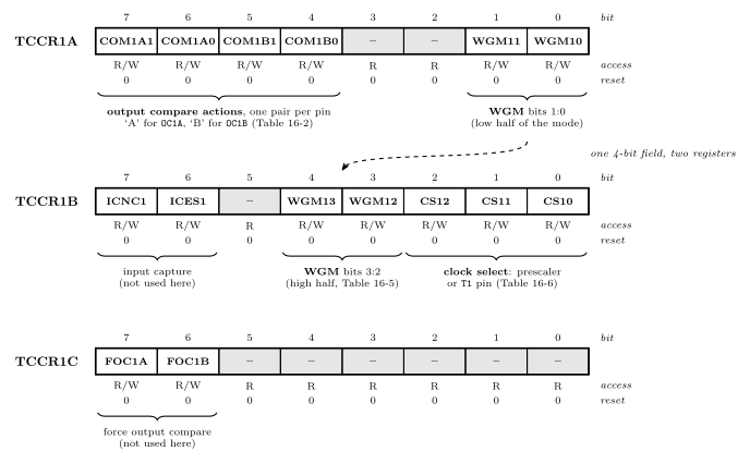
Figure 1: The three control registers of timer/counter 1 in the datasheet’s three-row form: bit numbers above, bit names in the boxes, access and reset value below. Grey boxes are reserved and read as 0. The bits that matter group into four fields, and one of them — the waveform generation mode — is split across two registers, WGM11:10 at the bottom of TCCR1A and WGM13:12 in the middle of TCCR1B, so a four-bit mode number has to be written in two halves. Everything a normal program sets lives in TCCR1A and TCCR1B; TCCR1C is left at 0.
The pattern to notice is that the register letter and the pin letter are different things. COM1A1 and COM1A0 are the two bits for pin OC1A; COM1B1 and COM1B0 are for OC1B; and both pairs live in TCCR1A.
The different “A”s
Names with an “A” in them:
| COMnA | OCnA | TCCRnA |
| OCRnA | OCIEnA | PINA |
| PORTA | ||
| DDRA |
These fall into three groups. The items in each group are related, but each group is independent of the others: the “A”s are different “A”s.
- Channel A of a timer —
COMnA(its output-compare action bits),OCRnA(its compare register),OCnA(its pin),OCIEnA(its interrupt enable). These four do go together: one compare channel, one letter. - Control register A —
TCCRnAis simply the first of the timer’s control registers. It holds channel B’s COM bits as well as channel A’s, so the A here is not the channel. - Port A —
PINA,PORTA,DDRAare a GPIO port and have nothing to do with timers at all.
There are 2 hard problems in computer science: cache invalidation, naming things, and off-by-1 errors. The off-by-one matters here: it is the + 1 in the master formula below, and Task 0 turns on it.
WGM — waveform generation modes
WGM11, WGM10 are bits 1 and 0 of TCCR1A; WGM13, WGM12 are bits 4 and 3 of TCCR1B (Figure 1).
Table 16-5 on page 138 of the datasheet describes the modes. Two are of interest:
- 0:
0000— normal. The count goes 0 → 1 → … → 65535 → 0 → … - 4:
0100— CTC, Clear Timer on Compare match. The counter resets to 0 when it reaches the value in theOCR1Aregister.
Mode 4 is the one that makes a timer programmable. In normal mode the period is fixed by the width — 65 536 counts, whatever the prescaler — and the only way to get a different period is to reload TCNT1 by hand. In CTC the period is OCR1A + 1 counts, chosen by the program, and the reset is done by the hardware. The fast PWM modes of Lecture 16 are the other members of this table (pulse-width-modulation).
The master formula
\[f_{\text{event}} = \frac{f_{\text{clk\_I/O}}}{N \cdot (\text{TOP} + 1)}\]
- \(f_{\text{clk\_I/O}}\) is the clock frequency of the device — 8 MHz for the ATmega324A.
- \(N\) is the prescaler.
- TOP is the maximum value that the timer will reach. This can be some fixed constant, or a value in an output compare register.
- \(f_{\text{event}}\) is the frequency of the event in question.
What event means, case by case:
- For hardware pin toggling, \(f_{\text{event}}\) is the frequency that the pin is toggled. The waveform consists of one falling edge and one rising edge. The frequency of that waveform is thus half of \(f_{\text{event}}\).
- For PWM (more on that in a later lab), \(f_{\text{event}}\) is the frequency of falling edges in non-inverting mode, and the frequency of rising edges in inverting mode.
- For interrupts (more on that in a later lab), \(f_{\text{event}}\) is the frequency that the interrupt runs.
Why the formula has the shape it does: the counter ticks at \(f_{\text{clk}} / N\) and each period is \(\text{TOP} + 1\) ticks long — from 0 up to TOP inclusive — so a period lasts \(N (\text{TOP}+1) / f_{\text{clk}}\) seconds and the event happens once per period. The \(+1\) is the off-by-one: TOP is the last value counted, not the number of values.
Worked: what is the frequency of this wave?
A sine wave is plotted on an axis marked 0 at the left and 1 at the right, and it completes three full cycles between the two marks. What is its frequency?
3 Hz. Three cycles per unit of time is 3 Hz, taking the unlabelled 0 and 1 as seconds. 6 Hz is wrong: it counts the half-cycles — each hump — which is the pin-toggling trap again: six edges per second is three cycles per second. 8 MHz is the AVR’s clock, not this wave.
Clock selection
CS12, CS11, CS10 are bits 2–0 of TCCR1B. From Table 16-6 on page 139 of the datasheet (here n = 1):
| CSn2 | CSn1 | CSn0 | Description |
|---|---|---|---|
| 0 | 0 | 0 | No clock source (Timer/Counter stopped) |
| 0 | 0 | 1 | clk\(_{\text{I/O}}\)/1 (No prescaling) |
| 0 | 1 | 0 | clk\(_{\text{I/O}}\)/8 (From prescaler) |
| 0 | 1 | 1 | clk\(_{\text{I/O}}\)/64 (From prescaler) |
| 1 | 0 | 0 | clk\(_{\text{I/O}}\)/256 (From prescaler) |
| 1 | 0 | 1 | clk\(_{\text{I/O}}\)/1024 (From prescaler) |
| 1 | 1 | 0 | External clock source on Tn pin. Clock on falling edge |
| 1 | 1 | 1 | External clock source on Tn pin. Clock on rising edge |
The T1 pin is port B, pin 1 (PB1, package pin 2, PCINT9/CLKO/T1; see p11 of the datasheet). The table is the clock-selection mux from Lecture 15: three bits pick one of eight inputs, and 000 is the stopped input, which is why writing zero to the CS bits is how a timer is switched off — and why a timer whose CS bits have not been set does nothing at all.
Clock selection — code example
Row 0 1 1 of the table — clk\(_{\text{I/O}}\)/64 (from prescaler) — is:
TCCR1B = (1<<CS11) | (1<<CS10);Bit labels can be used in code expressions. CS11 and CS10 are defined in the header as the bit numbers 1 and 0 (c-preprocessor-and-avr-headers), so (1<<CS11)|(1<<CS10) is 0b011 = 0x03, and the assignment also writes 0 to every other bit of TCCR1B — normal mode, no input capture. That is fine for this line but it is the reason Task 1 has to put its WGM bit in the same expression: a second TCCR1B = (1<<WGM12); would wipe the clock select out again (bit-masking).
Output compare actions — can toggle/clear/set pin
COM1A1, COM1A0, COM1B1, COM1B0 are bits 7–4 of TCCR1A. From Table 16-2 on page 136 of the datasheet (n = 1):
| COMnA1/COMnB1 | COMnA0/COMnB0 | Description |
|---|---|---|
| 0 | 0 | Normal port operation, OCnA/OCnB disconnected |
| 0 | 1 | Toggle OCnA/OCnB on Compare Match |
| 1 | 0 | Clear OCnA/OCnB on Compare Match (Set output to low level) |
| 1 | 1 | Set OCnA/OCnB on Compare Match (Set output to high level) |
The OC1A pin, for example, is PD5, package pin 19 (see p11 of the datasheet). Two things follow. Any non-zero COM value takes the pin away from the port — PORTD bit 5 no longer drives it, the timer does — so the pin changes from GPIO to timer/counter operation. And the pin still has to be made an output with DDRD, because the timer only decides the value, not the direction.
Tasks
Task 0
To toggle an output compare pin 8 times per second (4 Hz period) with timer/counter 1, what
- clock prescale
- output compare
values do we need?
Task 1 — Output Compare Based Timer
- Consider
lab12-1.c(on Blackboard). - The code is to toggle the OC1A pin (what pin is this?) 8 times per second (i.e. 4 Hz period).
- This pin is connected to an LED (e.g. LD0).
- Fill in the blanks to make the code work.
- Set up the hardware to do the work; software does nothing after that.
- Build and test your code on the AVR board.
- Look at the generated list (
lss) file for the assembly language equivalent.
Working — Task 0
“Toggle 8 times per second” is the event rate: \(f_{\text{event}} = 8\ \text{Hz}\). Each toggle is one edge, so the LED waveform has 4 rising edges a second — the task’s “4 Hz period” — and the pin-toggling rule (waveform frequency is half of \(f_{\text{event}}\)) is what reconciles the two numbers.
Put \(f_{\text{clk}} = 8\,\text{MHz}\) and \(f_{\text{event}} = 8\,\text{Hz}\) into the master formula and solve for the product:
\[N \cdot (\text{TOP} + 1) = \frac{8\,000\,000}{8} = 1\,000\,000\]
Then try each prescaler timer 1 offers:
| \(N\) | \(\text{TOP} + 1 = 10^6 / N\) | TOP | Usable? |
|---|---|---|---|
| 1 | 1 000 000 | 999 999 | no — timer 1 stops at 65 535 |
| 8 | 125 000 | 124 999 | no — too big for 16 bits |
| 64 | 15 625 | 15 624 | yes — exact |
| 256 | 3 906.25 | — | no — not a whole number |
| 1024 | 976.5625 | — | no — not a whole number |
So prescaler 64 (CS12:0 = 011) and OCR1A = 15624 in CTC mode, where TOP is OCR1A. It is the only combination that is both exact and fits, which is typical: the prescaler is chosen to bring TOP under 65 536, and then TOP is whatever the division leaves. The 256 and 1024 rows could be used at the cost of a fractional error (OCR1A = 3905 gives 8.00195 Hz), but the task wants the exact one.
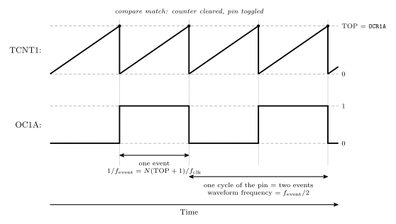
Figure 2: Clear-timer-on-compare mode with the output-compare pin set to toggle. The count climbs from 0 at the prescaled clock rate, reaches OCR1A (the TOP value), and is cleared to 0 by the hardware on the same tick that OC1A flips. One compare match is one event, so the events come at \(f_{\text{clk}} / (N(\text{TOP}+1))\) — but the pin only completes a full high-then-low cycle every two events, which is why the waveform on the LED runs at half the event frequency. With \(N = 64\) and \(\text{TOP} = 15624\) the matches are 125 ms apart and the LED cycle is 250 ms.
Working — Task 1
lab12-1.c is a Blackboard download with blanks to fill in. The task fixes what the blanks must produce, and the whole configuration is four register writes plus one direction bit, so the program is given in full here and can be matched against the download line by line.
What pin is OC1A? PD5 — package pin 19, PCINT29/OC1A. It has to be wired to an LED (LD0 on the IO board) and made an output.
#include <avr/io.h>

int main(void) {
  /* OC1A is PD5 - the timer decides its value, but it must be an output */
  DDRD |= (1<<5);

  /* Start counting from 0, and set the period: TOP = 15624 with N = 64
     gives 8 MHz / (64 * 15625) = 8 compare matches per second */
  TCNT1 = 0;
  OCR1A = 15624;

  /* Toggle OC1A on compare match: COM1A1:0 = 01.  WGM11:10 = 00. */
  TCCR1A = (1<<COM1A0);

  /* CTC mode: WGM13:12 = 01 (mode 4 = 0100).  Prescaler 64: CS12:0 = 011.
     This write starts the timer, so it comes last. */
  TCCR1B = (1<<WGM12) | (1<<CS11) | (1<<CS10);

  while(1) {
    /* Nothing.  The hardware toggles the pin; the CPU is idle. */
  }
}
Points where a blank is easy to get wrong:
- Mode 4 is
0100, split across the registers:WGM12is the only 1, and it is inTCCR1B(Figure 1).WGM11/WGM10inTCCR1Astay 0. - Toggle is
COM1A0alone (01), inTCCR1A. SettingCOM1A1instead gives clear on match (10), and the pin goes low once and stays there. - The clock-select bits and the WGM bit go in one assignment. Two separate
TCCR1B = …lines would each erase the other’s bits;|=on both would also work. OCR1A = 15624, not 15625. TOP is the last value counted; the period is TOP + 1 ticks.- Order:
OCR1Abefore the clock is started, so the first period is the right length;TCNT1 = 0is what reset leaves anyway, but writing it makes the intent visible.
Software does nothing after that — the while(1) body is empty and the LED blinks regardless. That is the point of the exercise: the timer is separate hardware, and a program that has set it up can go on to do anything else, or nothing.
The .lss file is the compiler’s listing, C source interleaved with the assembly it became. The five register writes appear as ldi/out for DDRD and TCCR1A… and ldi/sts pairs for OCR1A and TCNT1, high byte then low byte, exactly as under Accessing 16-bit I/O registers above; the empty loop is a single rjmp to itself (avr-program-structure).
Working — Task 2
lab12-2.c is also a Blackboard download with blanks to fill in. The task statement is enough to write the program, so what follows is a complete version that meets it; the download will have the same registers in its blanks.
Which pin is T0? From the pinout, T0 is on PB0 — package pin 1, PCINT8/XCK0/T0. (T1 is PB1, as in the clock-selection section.) The push button goes there, and it must be an input.
Two timers do two jobs:
- Timer/counter 0 counts the presses. Clock select
111— external clock source on T0 pin, clock on rising edge — in normal mode. Every rising edge onPB0adds one toTCNT0, with no software involved; the program just readsTCNT0when it wants the count. - Timer/counter 1 provides the 1 ms tick. CTC mode with
OCR1Afrom the master formula: \(f_{\text{event}} = 1000\,\text{Hz}\), so \(N(\text{TOP}+1) = 8000\); \(N = 8\), \(\text{TOP} = 999\). Nothing is wired toOC1Athis time — the program polls the compare-match flag,OCF1AinTIFR1, which the hardware sets on every match. The flag is cleared by writing a 1 to it.
#include <avr/io.h>

/* Seven segment display values */
uint8_t seven_seg[10] = { 63,6,91,79,102,109,125,7,127,111 };

int main(void) {
  uint8_t count;
  uint8_t left = 0;             /* which digit is lit this millisecond */

  DDRA = 0xFF;                  /* segments on port A            */
  DDRD |= (1<<0);               /* CC on PD0                     */
  DDRB &= ~(1<<0);              /* T0 = PB0 is an input          */

  /* Timer/counter 0: normal mode, clocked by rising edges on T0 */
  TCNT0 = 0;
  TCCR0A = 0;
  TCCR0B = (1<<CS02) | (1<<CS01) | (1<<CS00);

  /* Timer/counter 1: CTC, compare match every 1 ms
     8 MHz / (8 * (999+1)) = 1000 Hz */
  TCNT1 = 0;
  OCR1A = 999;
  TCCR1A = 0;
  TCCR1B = (1<<WGM12) | (1<<CS11);

  while(1) {
    count = TCNT0 % 100;        /* two digits' worth of the running count */

    if(left) {
      PORTA = seven_seg[count / 10];     /* tens */
      PORTD |= (1<<0);                   /* CC = 1: left digit */
    } else {
      PORTA = seven_seg[count % 10];     /* ones */
      PORTD &= ~(1<<0);                  /* CC = 0: right digit */
    }

    /* Wait for the 1 ms compare match, then clear the flag */
    while((TIFR1 & (1<<OCF1A)) == 0) {
    }
    TIFR1 = (1<<OCF1A);

    left = !left;               /* other digit next time */
  }
}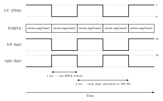
Figure 3: Display multiplexing on a 1 ms tick. The two digits share the eight segment lines, so only one can show its own pattern at a time; the program writes the tens pattern with CC high, waits 1 ms, writes the ones pattern with CC low, waits 1 ms, and repeats. Each digit is therefore lit half the time, at 500 Hz — far too fast for the eye to see it flicker, so both appear steady, at half brightness. Slow the tick to 250 ms and the same program visibly flips between the two digits, which is the task’s last step.
What each part is doing, and why:
TCCR0B = (1<<CS02)|(1<<CS01)|(1<<CS00)is row111of the clock-selection table, for timer 0. The button is the timer’s clock. A mechanical button bounces, so one press may register as several rising edges — the count can jump by two or three per press; that is the hardware being honest, not a bug in the code, and de-bouncing is a later problem.TCNT0 % 100— an 8-bit count runs 0–255, and two digits show 0–99, so the display shows the count modulo 100. Without this,count / 10reaches 25 and indexes past the end of the table (c-pointers-and-arrays).- The wait loop —
while((TIFR1 & (1<<OCF1A)) == 0)spins until the hardware sets the flag;TIFR1 = (1<<OCF1A)clears it by writing a 1 (a flag register clears the bits you write 1 to, the opposite of a port). The& (1<<OCF1A)is the test row of the bit-masking table from week8-lab-avr-c-programming. This is the software half of the compare match; Task 1 used the hardware half (the pin) and ignored the flag. - Segments before
CC. Each branch writes the pattern first and then selects the digit, so the newly selected digit never briefly shows the other digit’s pattern. left = !leftalternates;left ^= 1is the same thing spelled as an XOR mask.
Slowing it down — 4 times per second means a 250 ms tick: \(N(\text{TOP}+1) = 8\,000\,000 / 4 = 2\,000\,000\), and the only exact 16-bit fit is \(N = 64\), \(\text{TOP} = 31\,249\):
  OCR1A = 31249;
  TCCR1B = (1<<WGM12) | (1<<CS11) | (1<<CS10);   /* prescaler 64 */
Now the two digits are visibly taking turns, each on for a quarter of a second, and the multiplexing stops being an illusion.
See also
- avr-timers-and-counters — the three timer/counters, their registers, modes and the master formula
- pulse-width-modulation — the fast PWM modes, the other rows of the WGM table
- 2026-09-14-flow-of-control — Lecture 15: clock sources, prescaling and the clock-selection mux
- 2026-09-17-pulse-width-modulation — Lecture 16: the timer/counter summary and PWM
- seven-segment-display — the lookup table and
CC - bit-masking · c-operators · c-preprocessor-and-avr-headers —
(1<<CS11),|=,&= ~, and where the bit names come from - avr-io-ports · avr-architecture · timing-diagrams
- week8-lab-avr-c-programming — Lab 11, the seven-segment program these tasks extend
- avr-interrupts — the same timer 1 set-up driving an interrupt handler instead of a pin, with
TIMSK1andOCIE1A - week9-lab-avr-pwm — Lab 13, which carries on from here