Lab 11 — AVR C Programming
Learning Lab 11, the first lab in C. The seven-segment program from 2026-09-10-more-c-programming-on-the-avr is typed in, wired up and extended to hex digits and to a two-input adder. It also covers the bit-shift and bit-mask idioms that every AVR C program from here on is written in. See seven-segment-display for the display and its lookup table, bit-masking for the four masking operations, and c-operators for <<, |, & and ^.
What this lab covers
- Microchip Studio C programming
- AVR C programming exercises
Ed Lessons
The Ed discussion board also provides Ed Lessons, designed to instruct you in the basics of C. The content should be no more complex than CSSE1001 content. C programming for the AVR starts in week eight, with this lab.
The lessons are released in stages:
| Date | Lesson |
|---|---|
| 14 Aug | Basics |
| 28 Aug | Next Steps #1 |
| 11 Sep | Next Steps #2 |
| 25 Sep | Extension Tasks |
| 16 Oct | Floating Point Workshop |
The first three were out before this lab.
Worked: (23>>2)<<3
What is printed by this line of code:
printf("%d", (23>>2)<<3);
40.
Work it in binary, because the two shifts do not cancel:
| Step | Binary | Decimal |
|---|---|---|
23 |
1 0 1 1 1 |
23 |
23 >> 2 |
1 0 1 |
5 — the two low bits 11 fall off the end |
5 << 3 |
1 0 1 0 0 0 |
40 |
>> 2 is division by 4 with the remainder thrown away — \(\lfloor 23/4 \rfloor = 5\) — and << 3 is multiplication by 8, so the result is \(8 \cdot 5 = 40\), not \(23 \cdot 2 = 46\). The bits shifted out on the right are gone; shifting back left fills with zeros (c-operators). It is the same loss of information a lsr has in assembly, where the dropped bit lands in C and the next lsl shifts in a 0 (avr-instructions).
Bit shifts and AVR code
It is common to use bit-shifts to indicate which bits are being operated on.
Example: set bit 5 of port B to be an output and other bits to be inputs.
| Assembly language | C equivalent |
|---|---|
ldi r16, (1<<5) out DDRB, r16 |
DDRB = (1<<5); |
1<<5 makes it clear bit 5 is being set. Both are the constant 0b00100000 = 0x20; the assembler evaluates (1<<5) at assembly time exactly as the C compiler does, so neither line costs anything at run time. The point is legibility: 0x20 has to be decoded, 1<<5 says bit 5 in the source. The AVR header files name every register bit this way, which is why (1<<CS11) turns up in week8-lab-avr-timers.
Setting bits and keeping the rest
Example: set bits 3 and 4 of port B to be outputs whilst keeping the direction of the other bits the same.
Assembly language:
    in   r16, DDRB
    ori  r16, (1<<4)|(1<<3)
    out  DDRB, r16
C equivalent:
DDRB |= (1<<4)|(1<<3);This is shorthand for DDRB = DDRB | ((1<<4)|(1<<3)); (c-operators). Read the three assembly lines against it: in is the read of DDRB on the right-hand side, ori is the |, out is the assignment back. A read-modify-write is three instructions in assembly and one operator in C, and it is the difference between this example and the previous one: DDRB = (1<<5) replaces the register, forcing the other seven bits to 0, whereas |= adds the two bits to whatever was there. The mask (1<<4)|(1<<3) is 0b00011000 = 0x18.
Bit masking operations — more than just bitwise ANDs
The four operations of bit-masking, now in C:
| Operator | Does | Example |
|---|---|---|
Bitwise AND & |
Clear particular bits (e.g. zero out high 4 bits) | var = PINB & 0x0F; |
| Test particular bits (e.g. is bit 1 set?) | if(PINB & 0x02) … |
|
Bitwise OR \| |
Set particular bits (e.g. set sign bit to 1) | PORTC = PINB \| 0x80; |
Bitwise XOR ^ |
Invert particular bits (e.g. invert low 4 bits) | PORTC = PINB ^ 0x0F; |
The rule for building a mask is the same in every row: put a 1 on the bits the operation should touch — keep, for AND; set, for OR; flip, for XOR — and a 0 everywhere else. 0x0F appears twice with two meanings: with & it keeps the low nibble, with ^ it inverts it.
The test row is the one that is new. PINB & 0x02 is 0x02 if bit 1 is set and 0x00 if not, and since C treats any non-zero value as true (c-control-flow) that expression can sit directly inside an if. It does not need to be compared with 1 — and must not be, because it never is 1.
Seven segment display
- LEDs arranged in a pattern
- Eight segments if DP (decimal point) is included
- One byte drives it, e.g.
0001 1110₂ with the “A” segment as LSB and the “DP” segment as MSB
The segments are lettered A across the top, B upper right, C lower right, D bottom, E lower left, F upper left, G across the middle, and DP the dot — the same lettering as seven-segment-display, just in capitals. With A at bit 0 and DP at bit 7 the byte reads, MSB first, DP G F E D C B A, so 0001 1110 lights E, D, C and B: the right-hand side, the bottom and the lower left — a shape like a J.
Worked: what 0011 1110₂ then 1111 0100₂ spell out (“A” = LSB)
“Uh.”
| Byte | DP G F E D C B A |
Lit | Shows |
|---|---|---|---|
0011 1110 |
0 0 1 1 1 1 1 0 |
F E D C B | U |
1111 0100 |
1 1 1 1 0 1 0 0 |
DP G F E C | h with the dot: h. |
In the second byte, F, E and G make the left-hand upright and the middle bar; C adds the lower right; no A, so the top is open and the shape is a lowercase h rather than an H. Bit 7 lights the decimal point after it. Task 2 turns this reading-off into writing the six hex letters.
Tasks
Task 1 — Seven Segment Display
- Create an AVR C project and type in and build the seven-segment display (SSD) example from lecture 14. The code is also on Blackboard.
- Connect up AVR pins to the IO board pins:
- Connect IO board SSD inputs (A to G and DP) to port A (you can use 2 × 4-way cables and headers for this. SSD pin A should be connected to the least significant bit of port A.)
- Connect IO board pin CC (SSD digit select input) to button B0
- Connect IO board switches 0 to 3 to the lower four pins of port C
- Download your program to the board and test it — check that the number you enter on switches 0 to 3 shows up as a digit on the seven-segment display. Press and release button B0 and check that the number shows up on the other SSD digit.
Task 2 — Adding Hex Patterns
- Modify the task 1 code so that your program can also output values 10 to 15 as hex digits as shown in the following patterns: A b C d E F.
- Build, download and test your program.
Task 3 — Addition Results on SSD
- Write a program that repeatedly reads the lower 4 bits of port A and the lower 4 bits of port B and adds these two values together and displays (on the SSD, using a port of your choice) the hexadecimal value of the lower 4 bits of the result.
- Wire up the IO board and AVR 324 Dev board as required.
- Build, download and test your program.
Task 4 — Bitmasking
- Download
lab11-task4.cfrom Blackboard - Read through the comments at the start of the code
- Run the code as-is and observe the issues
- Fix the code by bitmasking where required
- Interrupts will be explained in Lec 17 then Lab 14
Working — Task 1
The project. In Microchip Studio a C project is a GCC C Executable Project for the ATmega324A, the same device selection as the assembly projects of week5-lab-avr-assembly-one; the file it gives you is main.c. The program is the one from Lecture 14, unchanged:
#include <avr/io.h>

/* Seven segment display values */
uint8_t seven_seg[10] = { 63,6,91,79,102,109,125,7,127,111};

int main(void) {
  uint8_t digit;

  /* Set port A pins to be outputs, port C pins to be inputs */
  DDRA = 0xFF;
  DDRC = 0;    /* This is the default, could omit. */
  while(1) {
    /* Read in a digit from lower half of port C pins */
    /* We read the whole byte and mask out upper bits */
    digit = PINC & 0x0F;
    /* Write out seven segment display value to port A */
    if(digit < 10) {
      PORTA = seven_seg[digit];
    } else {
      PORTA = 0;
    }
  }
}
Every line is explained in 2026-09-10-more-c-programming-on-the-avr. The new part is the wiring, and the wiring has one rule that the code silently depends on: SSD pin A goes to PA0. The lookup table was built with segment a at bit 0 and dp at bit 7, so the cable must carry that order across — A on PA0 up through G on PA6 and DP on PA7. Get the two 4-way cables swapped and every digit comes out scrambled.
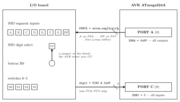
Figure 1: The three connections Task 1 asks for, and what each one means for the program. Port A carries the eight segment lines in the same order as the bits of the lookup table, so PORTA = seven_seg[digit] lights a digit with no further translation. The low four bits of port C read the switches, and & 0x0F discards the four unconnected pins above them. The CC line is not driven by the AVR at all: it is jumpered to button B0 on the board, so the button alone decides which of the two digits shows the pattern — which is why pressing it moves the number across without the program doing anything.
Testing (c). Set a number on switches 0–3 and the matching digit should appear. The interesting test is the button: CC is wired to B0, not to the AVR, so pressing it changes the common-cathode select in hardware and the same pattern appears on the other digit — the program has not changed, only which digit’s cathode is connected (seven-segment-display). Switch values 10–15 blank the display, which is the else branch doing its job; Task 2 is about making them show something instead.
Working — Task 2
Six more entries and the display can show every value four bits can hold. The patterns are A b C d E F, and the case is not cosmetic. An uppercase B on seven segments is indistinguishable from 8, and an uppercase D from 0, so those two are drawn lowercase; the other four have no such clash and stay capitals.
| Digit | Segments lit | dp g f e d c b a |
Decimal |
|---|---|---|---|
| A | a b c e f g | 0111 0111 |
119 |
| b | c d e f g | 0111 1100 |
124 |
| C | a d e f | 0011 1001 |
57 |
| d | b c d e g | 0101 1110 |
94 |
| E | a d e f g | 0111 1001 |
121 |
| F | a e f g | 0111 0001 |
113 |
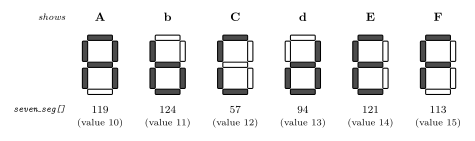
Figure 2: The six hex letters as seven-segment patterns, with the byte that produces each one in decimal underneath, ready to append to the lookup table. Heavy segments are lit; the bit order is dp g f e d c b a with a at bit 0, as for the ten decimal digits. The letters b and d are the lowercase forms because their capitals would be indistinguishable from 8 and 0 on this display: b is 8 without segments a and b, d is 0 with the top-left corner (a, f) removed and the middle bar g added.
The change to the program is two lines: the table grows to sixteen entries, and the guard is no longer needed because four input bits cannot index past it.
#include <avr/io.h>

/* Seven segment display values: 0-9 then A b C d E F */
uint8_t seven_seg[16] = { 63,6,91,79,102,109,125,7,127,111,
                          119,124,57,94,121,113 };

int main(void) {
  uint8_t digit;

  DDRA = 0xFF;                 /* segments out on port A */
  DDRC = 0;                    /* switches in on port C */
  while(1) {
    digit = PINC & 0x0F;       /* 0 to 15 - every value is now a valid index */
    PORTA = seven_seg[digit];
  }
}
Dropping the if is safe only because of the mask on the line above it: PINC & 0x0F is at most 15 and seven_seg[15] exists. Leaving the guard in as if(digit < 16) costs nothing and documents the assumption; taking the mask out would be the bug (c-pointers-and-arrays — C will not stop an index at 16).
Working — Task 3
Two 4-bit inputs, one 4-bit output. The task fixes the inputs — low nibble of port A, low nibble of port B — and leaves the output port to you; port C is used here, the port Task 1 used for input, with the SSD moved across to it. Port D would do equally well.
#include <avr/io.h>

/* 0-9 then A b C d E F, as in Task 2 */
uint8_t seven_seg[16] = { 63,6,91,79,102,109,125,7,127,111,
                          119,124,57,94,121,113 };

int main(void) {
  uint8_t a, b, sum;

  DDRA = 0;                    /* switches 0-3 on PA0-PA3 */
  DDRB = 0;                    /* switches 4-7 on PB0-PB3 */
  DDRC = 0xFF;                 /* SSD segments on port C  */
  while(1) {
    a = PINA & 0x0F;           /* extract the low nibble of each port */
    b = PINB & 0x0F;
    sum = (a + b) & 0x0F;      /* add, then keep the low 4 bits of the result */
    PORTC = seven_seg[sum];    /* show it as a hex digit */
  }
}
Three things the wording of the task decides:
- Both masks are needed, not just one. The upper four pins of each port are unconnected and read as unpredictable values, so without the
& 0x0Fthe sum would include junk (week6-lab-avr-io-ports hit the same thing withandi). - The result is masked too. The largest sum is \(15 + 15 = 30\), which fits comfortably in a
uint8_t, so nothing overflows in C; but the task asks for the lower 4 bits of the result, so bit 4 — the carry out of the nibble — is discarded. $9 + 9 = 18 = $0x12shows as 2, and $8 + 8 = 16 = $0x10shows as 0. That is the answer, not a bug: it is the four-bit adder of 2026-08-04-binary-arithmetic with its carry-out unconnected. - The hex table from Task 2 is what makes it display. Sums of 10 to 15 are common (7 + 5, say), and they must show as hex letters, which is why the task follows Task 2 rather than preceding it.
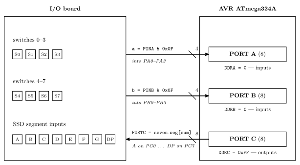
Figure 3: The Task 3 wiring. Two nibbles of switches come in on the low halves of ports A and B, the SSD segment lines go out on port C, and the direction registers follow: 0 for the two input ports, 0xFF for the output port. The upper four pins of ports A and B are left unconnected, which is what makes the & 0x0F on each read necessary rather than decorative. CC can be left tied to a button as in Task 1; the program only ever drives one digit.
Testing. With all eight switches down the display shows 0; raise switch 0 alone and it shows 1, switch 4 alone and it also shows 1 (that is the other operand); switches 0 and 4 together show 2. Setting both nibbles to 1111 shows E: $15 + 15 = 30 = $ 0x1E, low nibble E.
Working — Task 4
lab11-task4.c is a Blackboard download. The exercise is a program that runs but misbehaves, where every fault is a whole-port write or read that should have been a masked one. The toolkit for fixing it is the bit-masking table above, applied at the points where a program touches only some of a port’s pins:
| Symptom | Likely line | Fix |
|---|---|---|
| Setting one pin’s direction disturbs the others | DDRx = (1<<n); |
DDRx \|= (1<<n); |
| Writing one output changes neighbouring outputs | PORTx = value; |
PORTx = (PORTx & ~mask) \| (value & mask); — or \|= / &= for a single bit |
| An input test is never true | if(PINx & (1<<n) == 1) |
if(PINx & (1<<n)) — the result is 1<<n, not 1 |
| Unconnected pins leak into a value | var = PINx; |
var = PINx & 0x0F; |
The third row is the test case from the bit-masking table: PINB & 0x02 is either 0x02 or 0, and comparing it to 1 is always false.
Interrupts are explained in Lecture 17, then Lab 14. The downloaded file presumably contains an interrupt handler, which is to be left alone for now; only the masking is to be fixed. Lecture 17 is 2026-09-21-interrupts, and what an ISR(...) function is and how it gets called is in avr-interrupts.
See also
- seven-segment-display — segment lettering, the ten digit codes, and
CC - bit-masking — clear, test, set and invert, and why the masks are what they are
- c-operators —
<<,>>,&,|,^, and the|=shorthand - c-control-flow — why
if(PINB & 0x02)works without a comparison - avr-io-ports · io-board · c-preprocessor-and-avr-headers
- 2026-09-10-more-c-programming-on-the-avr — Lecture 14, where the Task 1 program comes from
- week6-lab-avr-io-ports — Lab 10, the same wiring exercises in assembly
- week8-lab-avr-timers — Lab 12, where
(1<<CS11)and friends configure a timer - avr-interrupts — the
ISR()handlers the lab code contains