Lecture 16 — Pulse Width Modulation
The timer/counters introduced at the end of Lecture 15 (2026-09-14-flow-of-control), now put to their main use: generating a pulse-width-modulated signal on a pin, entirely in hardware, so that a digital output can behave like an adjustable analog one. The first part completes the timer material: what a timer is for, which pins it owns, which registers configure it, and its three modes of operation. The rest is PWM itself and the two Fast PWM modes of timer/counter 0. The evergreen notes are avr-timers-and-counters and pulse-width-modulation.
Timer/counters — the three jobs
The block diagram has three timer/counter blocks that matter, numbered 0, 1 and 2; the T/C 3 block is not used (avr-architecture).
An 8-bit timer counting up from 0 at the 8 MHz system clock with no prescaling takes
\[T = \frac{255}{8 \cdot 10^{6}} = 30\ \mu\text{s}\]
This is rounded down from the 32 µs the arithmetic gives (\(256 / 8\,\text{MHz} = 32\ \mu\text{s}\) for the full 256 counts). It is the shortest period the timer can produce, and every other period comes from lengthening it.
A timer/counter is for three things:
- Timing, e.g. toggling an LED every 10 ms. The count climbs from 0 to 255 again and again, driven by the 8 MHz clock. A compare value in OCR, say 128, is crossed once per sweep, halfway up. The crossing is a regular event, and a pin can be driven high (1) or toggled on it.
- Counting an external signal. Each step is an external pulse, not a clock tick. With OCR at 100, the crossing means 100 pulses have arrived.
- Pulse width modulation (PWM): a pulse train on a pin.
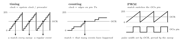
Figure 1: The three jobs of a timer/counter, all built from the same two parts: a count that climbs, and a compare register that marks a value on the way up. Timing: the count is driven by the system clock, so each sweep takes a fixed time and the compare match is a regular event, good for toggling a pin or an LED every so many milliseconds. Counting: the count is driven by edges on an external pin, so the match means a fixed number of events has occurred. PWM: the match is used to switch an output pin partway through every sweep, so the pin carries a pulse whose width is set by the compare value. The hardware does all three without the CPU touching the count.
Timer/counters — separate hardware, configured through I/O registers
A timer/counter:
- can be used to perform actions with pre-defined timing, e.g. do some action every 100 ms;
- can be used to generate PWM;
- can be used to count pulses (logic transitions on a given pin);
- is separate hardware to the CPU;
- is tied to particular pins on the microcontroller. Configuring the timer/counter changes these pins from their default GPIO operation to timer/counter operation;
- is configured by reading and writing I/O registers:
| Register | Kind |
|---|---|
| Timer/Counter register | data: the current value of the count |
| Control registers | control |
| Output compare registers | control |
| Interrupt registers | interrupt |
Every I/O register met so far is one of the same three kinds:
\[\text{I/O reg} \leftarrow \begin{cases} \text{data} & (\texttt{PORT}, \texttt{PIN}, \texttt{TCNT}) \\ \text{control} & (\texttt{DDR}, \texttt{OCR}, \texttt{TCCR}\ldots) \\ \text{interrupt} & (\texttt{TIMSK}, \texttt{TIFR}\ldots) \end{cases}\]
A timer is another peripheral configured through I/O registers, exactly like a port. TCNT is the timer’s PIN, the value you read. TCCR and OCR are its DDR, how it is set up. The interrupt registers are new and are covered in Lecture 17 (2026-09-21-interrupts, avr-interrupts). Separate hardware is the important property: once configured, the timer counts, compares and drives its pin with the CPU doing nothing, which is what makes hardware PWM free.
Timer/counters — the pins
Pins 1–8, at the top left of the pinout, are GPIO port B. Six pins carry the output-compare functions:
| Timer | Pins |
|---|---|
| 0 | PB3 = OC0A, PB4 = OC0B |
| 1 | PD5 = OC1A, PD4 = OC1B |
| 2 | PD7 = OC2A, PD6 = OC2B |
Each timer has two compare units, A and B, each with its own register and its own pin. The two give two independent match events per sweep of one counter. With OCR0A = 200 and OCR0B = 128, timer 0’s count from 0 to 255 crosses both values on every sweep, and each crossing is its own match.
AVR timers/counters summary — ATmega324A
| Timer/Counter 0 | Timer/Counter 1 | Timer/Counter 2 | |
|---|---|---|---|
| Pins | PB3 (OC0A) & PB4 (OC0B) | PD5 (OC1A) & PD4 (OC1B) | PD7 (OC2A) & PD6 (OC2B) |
| Width | 8-bit (counts to 255) | 16-bit | 8-bit |
| Supports PWM | ✓ | ✓ | ✓ |
| Modes of operation | Normal, CTC, Fast-PWM, phase correct PWM | Normal, CTC, Fast-PWM, PC-PWM and PFC-PWM | Normal, CTC, Fast-PWM and phase correct PWM |
| Clock prescaler (\(PRE\)) | No clock, F, F/8, F/64, F/256, F/1024 | No clock, F, F/8, F/64, F/256, F/1024 | No clock, F, F/8, F/32, F/64, F/128, F/256, F/1024 |
| I/O registers | TCNT0 (data); TCCR0A, TCCR0B, OCR0A, OCR0B (control); TIMSK0, TIFR0 (interrupt) |
TCNT1H, TCNT1L; TCCR1A, TCCR1B, TCCR1C; OCR1AH, OCR1AL, OCR1BH, OCR1BL; TIMSK1, TIFR1 |
TCNT2; TCCR2A, TCCR2B; OCR2A, OCR2B; TIMSK2, TIFR2 |
The three modes that matter:
| Mode | Behaviour |
|---|---|
| Normal | the count climbs from 0 to 255 and wraps to 0. It runs freely; a compare value (say OCR = 128) is just a marker on the way |
| CTC — clear on compare | the count resets when it reaches OCR, so the compare value becomes the top of the count |
| PWM | the output is a pulse train |
Timer 1 is 16 bits wide, so every one of its data registers is a pair of bytes with H and L suffixes, and it has a third control register, TCCR1C. Timers 0 and 1 have the same prescaler list. Timer 2’s list adds F/32 and F/128, the two extra taps met in Lecture 15. The register-by-register detail, and Lab 12’s walk through TCCR1A/B/C, are in avr-timers-and-counters and week8-lab-avr-timers.
Pulse width modulation (PWM)
PWM is varying the duty cycle of a periodic pulse. The duty cycle is the percentage of time that the signal is on (high):
\[\text{duty cycle} = \frac{T_{ON}}{T} \cdot 100\%\]
The pulse train switches between 5 V and 0. \(T\) is one full period, in seconds, and \(T_{ON}\) is the high part of it. The frequency is \(f = 1/T\), in Hz. At the same period, a duty cycle of 0 % is flat low, 25 % a narrow pulse, 50 % a square wave, 75 % a wide pulse and 100 % flat high.
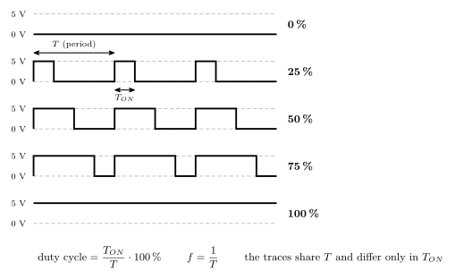
Figure 2: One period of a PWM signal and the two numbers that describe it. The period \(T\) is fixed and sets the frequency \(f = 1/T\); the on-time \(T_{ON}\) is the part of each period the output spends high. Their ratio is the duty cycle. The five traces have the same period and differ only in \(T_{ON}\): from 0,% (never high) through a square wave at 50,% to 100,% (never low). Modulating the pulse width means moving \(T_{ON}\) while leaving \(T\) alone, which is exactly what changing a compare register does.
PWM — average value
If the periodic pulse is “fast enough”, the signal looks like its average value. The average rises with the duty cycle: the 75 % waveform has a higher average than the 50 % one, and the 50 % one a higher average than the 25 % one. So PWM can be used to control the average voltage delivered to a load, for example to control the speed of a DC motor.
The average over one period, for a 5 V pulse:
\[V_{avg} = \frac{\int_0^{T} v(t)\,dt}{T} = \frac{\int_0^{T_{ON}} 5\,dt}{T} = \frac{T_{ON}}{T} \cdot 5 \;\propto\; \text{duty cycle}\]
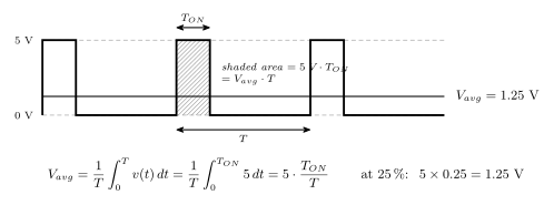
Figure 3: Why a PWM signal has an average, and why it is proportional to the duty cycle. The average of any periodic voltage is the area under one period divided by the period. For a pulse the area is a rectangle, \(5,\text{V} \times T_{ON}\), so dividing by \(T\) leaves \(5,\text{V} \times T_{ON}/T\): the supply voltage scaled by the duty cycle. A load that cannot follow the individual pulses — a motor’s inertia, an LED as seen by the eye, a loudspeaker cone — responds to this average and not to the pulses, which is how a pin that is only ever at 0 V or 5 V delivers 1.25 V.
Fast enough means the load has to be slow compared with the period: a motor’s inertia, a lamp’s thermal mass, the eye’s persistence, or an explicit low-pass filter. If the period is long enough for the load to follow the pulses, it sees pulses. So the PWM frequency is chosen for the load, and then the duty cycle is the only thing varied.
PWM — an average that changes over time
The pulse width can be varied so that the “average value” changes over time. A train of pulses whose widths grow and shrink has an average that follows a sine wave, a sine tone: the pulses are wide at the peak and narrow at the trough. Vary \(T_{ON}\) smoothly from period to period and the average traces out whatever waveform you like; filter off the pulses and that waveform is what comes out. This is how PWM generates audio.
Uses of PWM
PWM is useful for generating signals that look analog from a purely digital source. It can be used for:
- varying the brightness of lights/LEDs (e.g. fading)
- motor control (variable speed)
- generating audio (with appropriate filtering)
The AVR has no digital-to-analog converter; PWM plus the load’s own filtering is how it gets an analog-looking output.
LED brightness fading
Take two pulse trains driving an LED, one with a large duty cycle and one with a small one. Each has its own \(V_{avg}\), and the one with the large duty cycle has the higher \(V_{avg}\). Brightness rises with \(V_{avg}\), so it gives the brighter LED. A wider pulse means a higher average current, and the eye — the low-pass filter in this case — sees a brighter LED. Fading is ramping the duty cycle.
PWM on the AVR: Fast PWM mode (example with Timer/Counter 0)
Fast PWM has two options, chosen by the Waveform Generation Mode bits. The other modes are in Lab 12 (week8-lab-avr-timers), which introduced modes 0 (normal) and 4 (CTC) for timer 1.
The two options are two values of the three WGM bits. In each, the timer value against time is a sawtooth, the compare register is a horizontal line across it, and the pin’s waveform sits underneath:
Mode 3: WGM[2:0] = 011 (0x3) |
Mode 7: WGM[2:0] = 111 (0x7) |
|
|---|---|---|
| Top of the count | 255 — the counter always sweeps 0 to 255 | OCR0A — TOP is OCR0A in place of 255; the count sweeps 0 to OCR0A |
| Compare line | OCR0A or OCR0B, the Output Compare Register values. Can have two separate PWMs on one timer |
OCR0A sets the top, OCR0B sets the pulse |
| Pin waveform | for one compare value, say 100, there are two waveforms: inverting and non-inverting — the same match, the opposite polarity, each with its own pulse width | the high part of the waveform is the duty cycle; the period is now the shorter sweep |
The count is a sawtooth, the compare register is a horizontal line across it, and the pin changes state where they cross. The crossing moves up and down the ramp as the register value changes, and that moves the edge of the pulse, which is what modulating the width means. Whether the pin goes high or low at the crossing is a separate choice, the COM bits, and gives the inverting and non-inverting pair. Mode 3 fixes the period at 256 counts; mode 7 lets OCR0A shorten it, at the price of one of the two compare units.
Fast PWM mode — WGM[2:0] = 011 (0x3)
The count climbs from 0 to 255, so one period is 256 ticks. One tick lasts
\[T_{tick} = \frac{1}{CLK / PRE}\]
so the period and the frequency are
\[T = \frac{256}{CLK / PRE} \qquad\qquad f = \frac{CLK}{256 \cdot PRE}\]
Take a compare value of 191. The gap between it and 255 is 64 counts, so
\[\text{duty cycle} = \frac{T_{ON}}{T} = \frac{64}{256} \cdot 100\% = \mathbf{25\%}\]
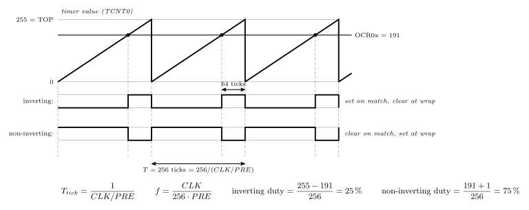
Figure 4: Fast PWM with a fixed top of 255 (mode 3, WGM[2:0] = 011) on an 8-bit timer. The count climbs one step per prescaled clock tick from 0 to 255 and wraps, so every period is exactly 256 ticks and the frequency is \(CLK/(256 \cdot PRE)\) regardless of the compare value. The compare register draws a line across the ramp; the pin switches at the crossing and switches back at the wrap. In inverting mode the pin goes high at the match and low at the wrap, so it is high for \(255 - OCR\) ticks; with \(OCR = 191\) that is 64 ticks of 256, a 25,% duty cycle. Non-inverting mode is the same crossing with the polarity swapped: high for \(OCR + 1\) ticks, 75,% here. The two outputs always add up to a full period, so the two modes are one signal and its complement.
Reading the formulas. The prescaler sets the tick, the fixed 256-count sweep sets the period, and only the compare value moves the edge. So in mode 3 frequency and duty cycle are set by different registers and do not interact, which is convenient. The cost is that the frequency can only take the eight values \(CLK/(256 \cdot PRE)\) allows: at 8 MHz, from 31.25 kHz down to 30.5 Hz. If none of those is right, mode 7.
Fast PWM mode — WGM[2:0] = 111 (0x7)
The count now climbs from 0 to OCR0A, which is 1 + OCR0A ticks. TOP is OCR0A, not 255. Take OCR0A = 127 and OCR0B = 95, a gap of 32 counts.
\[T_{tick} = \frac{1}{CLK / PRE} \qquad\qquad T = \frac{1 + OCR0A}{CLK / PRE} \qquad\qquad f = \frac{CLK}{(1 + OCR0A) \cdot PRE}\]
\[\text{duty cycle} = \frac{32}{128} \cdot 100\% = \mathbf{25\%}\]
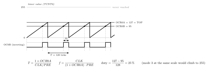
Figure 5: Fast PWM with OCR0A as the top (mode 7, WGM[2:0] = 111). The count now wraps when it reaches OCR0A instead of 255, so the period is \(OCR0A + 1\) ticks and can be chosen freely instead of being fixed at 256; the frequency becomes \(CLK/((OCR0A+1)\cdot PRE)\). The pulse is generated on the other compare unit: OCR0B draws the line across the shorter ramp and the OC0B pin switches at that crossing. With \(OCR0A = 127\) and \(OCR0B = 95\) the period is 128 ticks and the inverting output is high for \(127 - 95 = 32\) of them, again 25,%. Compare unit A is spent on setting the period, so mode 7 buys frequency control by giving up one of the two PWM outputs; OC0A can at most toggle at each wrap.
The trade. Mode 3 gives two PWM outputs at a fixed frequency; mode 7 gives one PWM output at a chosen frequency. The general formula behind both, \(f = CLK / (PRE \cdot (TOP + 1))\), is the master formula Lab 12 works from, with \(TOP\) = 255 or \(OCR0A\) as the mode dictates (avr-timers-and-counters).
Phase correct PWM
- The centres of the pulses remain at the same point in the period. At 25 %, 50 % and 75 % the centres line up.
- It is better for motor speed control.
- It is implemented by having the timer count up and then down.
- It is not used in this course, which uses fast PWM mode only.
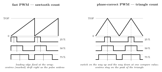
Figure 6: Fast PWM against phase-correct PWM, for the same three duty cycles. In fast PWM the count is a sawtooth and every pulse starts at the wrap, so its leading edge is fixed and widening the pulse moves only the trailing edge: the pulse’s centre drifts as the duty cycle changes. In phase-correct PWM the count climbs and then descends, and the pin switches on the way up and back on the way down at the same compare value, so the pulse is symmetric about the peak of the triangle: its centre stays put and both edges move outward together. For a motor that is smoother, because the current pulse’s timing relative to the period does not shift as the speed is changed; the price is that the triangle takes twice as long, halving the frequency. This course uses fast PWM only.
Counting up and then down is the whole mechanism: the compare line is crossed twice per triangle, once rising and once falling, and the two crossings are equidistant from the peak. Nothing in the labs or the assignment needs it; fast PWM is the mode the course uses, and it is the one Lab 12’s master formula and the WGM tables describe.
See also
- pulse-width-modulation — duty cycle, average value, the two fast PWM modes and their formulas, inverting versus non-inverting
- avr-timers-and-counters — the three timers, their registers, prescaler, modes and pins
- 2026-09-14-flow-of-control — Lecture 15, where the timers were introduced
- week8-lab-avr-timers — Lab 12:
TCCR1A/B/C,WGM,CSandCOMbit by bit, and the master formula - week9-lab-avr-pwm — Lab 13: PWM on the board
- avr-io-ports · avr-architecture · timing-diagrams · counters