CSSE2010 — Week 10 Notes
Lecture 19 — More I/O
Two more ways for a microcontroller to talk to other chips, and the habits that make I/O code correct and readable. The first half is about buses: which device is in charge of a transfer, the two-wire I²C bus (TWI on the AVR), and SPI, a synchronous serial bus built from two shift registers joined in a ring, with the ATmega324A’s SPI port, its pins and its clock rates, and bit bashing for when the hardware is missing. The second half is AVR I/O coding: volatile for variables an interrupt handler changes, and setting, clearing and toggling bits of I/O registers by name. The reference notes are serial-communication, avr-spi, bit-masking and avr-io-ports.
Goals
- Say what makes a device a bus master or a bus slave, and why memory is always a slave.
- Describe the I²C bus and find the ATmega324A’s TWI pins.
- Explain how SPI sends a byte each way at once, using two shift registers joined in a ring.
- Connect several SPI slaves to one master, with a select line each or as a daisy chain.
- Find the SPI pins on the ATmega324A and work out an SPI clock rate from its divider.
- Say what bit bashing is and when it is the answer.
- Declare a variable
volatilewhen an interrupt handler changes it, and say what the optimiser does otherwise. - Set, clear and toggle single bits of an I/O register, with the bits named.
Bus masters and slaves
When several devices share wires, one of them has to decide when a transfer happens and which way it goes.
- The master is the device that initiates and controls the transfer of data. It decides when a transfer starts and which device it is with, and on a synchronous bus it also drives the clock.
- A slave waits for requests and responds to the master. It never starts a transfer of its own.
The roles belong to a transfer, not to a device for all time. Some devices can be masters and slaves, at different times. The ATmega324A’s SPI port and its TWI port can each be set up as either.
Memory can never be a bus master. It only ever answers a read or a write of an address that something else has chosen. On the AVR’s memory bus the CPU is the master and the memories are slaves.
Check. A CPU, a memory chip and an ATmega324A’s SPI port are on buses together. Which of them could start a transfer? The CPU, always. The SPI port, when it is set up as a master. The memory, never: it has no way to begin anything, only to answer.
I²C and TWI
I²C is the Inter-Integrated Circuit bus, created by Philips Semiconductor, now NXP. TWI, the Two-wire Interface, is the name Atmel uses for it. Both are synchronous serial: one of the wires is a clock (serial-communication).
Every device on the bus, device 1 to device n, connects to the same two wires:
| Wire | Carries |
|---|---|
| SDA | serial data, in either direction |
| SCL | serial clock, driven by the master |
Two wires serve many devices, and adding one adds no wires. The price is that every device sees every transfer, so the master begins each one by sending the address of the slave it wants, and the others ignore it. With one data wire, data goes one way at a time. The bus is drawn, with the pull-up resistors that make the sharing work, in serial-communication.
TWI on the ATmega324A
- The ATmega324A has one TWI port.
- Its two wires are an alternate use of two port C pins: PC0 is SCL and PC1 is SDA. While the TWI is switched on, those pins belong to it, not to
PORTC. - The datasheet describes the TWI in full on pages 211 to 239.
SPI
SPI is the Serial Peripheral Interface. The master and the slave each hold an 8-bit shift register (shift-registers), and the wires join the two registers into one ring. There are four signals:
| Signal | Driven by | Carries |
|---|---|---|
| SCK (also written SCLK) | master | the serial clock, one pulse per bit |
| MOSI | master | Master Out, Slave In: data to the slave |
| MISO | slave | Master In, Slave Out: data to the master |
| \(\overline{\text{SS}}\) | master | Slave Select, active low: 0 selects the slave |
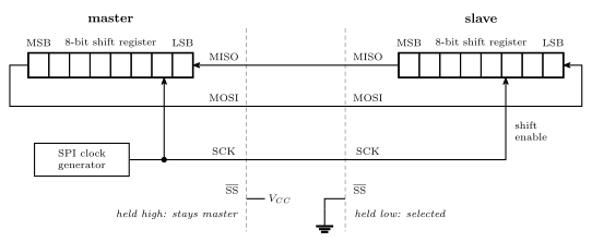
Figure 1: SPI as two 8-bit shift registers joined in a ring. Each pulse of SCK, made by the master’s clock generator, shifts both registers one place towards the MSB. At the slave, SCK is the register’s shift enable, so the slave’s register moves only when a pulse arrives from the master. The master’s MSB leaves on MOSI and enters the slave at its LSB, while the slave’s MSB leaves on MISO and enters the master at its LSB. After eight pulses the two bytes have changed places, so every transfer moves a byte in each direction. The dashed lines are the edges of the two chips, with the pin names just inside them and the wiring between. The slave’s \(\overline{\text{SS}}\) is tied to ground, so it is always selected; the master’s own \(\overline{\text{SS}}\) is tied to \(V_{CC}\), which keeps it a master.
How the ring moves a byte. On each clock pulse both registers shift one place towards the MSB, at the same moment. At the slave, SCK is the register’s shift enable: the slave’s register moves only when a pulse arrives from the master. The bit that falls off the master’s MSB end goes out on MOSI and into the slave’s LSB end; the bit that falls off the slave’s MSB end goes out on MISO and into the master’s LSB end. Neither register gains or loses anything overall: the two of them are a single 16-bit register rotating. After eight pulses every bit has moved eight places, which carries the master’s byte entirely into the slave and the slave’s byte entirely into the master.
So every SPI transfer is an exchange. To read a byte from a slave the master has to send one, even a meaningless one, and every byte sent brings one back, which the master may simply ignore.
The master’s clock generator decides when every bit moves, so the slave never has to time a bit for itself, and nothing has to be agreed about speed beyond the fastest the slave can follow. That is the advantage of a synchronous link over a UART, where both ends must be set to the same baud rate beforehand.
Worked: one exchange
The master’s register holds 0x4D and the slave’s holds 0x73, most significant bit first. What travels on each data wire, and what does each register hold after eight clocks?
MOSI carries the master’s byte, MSB first: 0 1 0 0 1 1 0 1. MISO carries the slave’s: 0 1 1 1 0 0 1 1. After eight clocks the master holds 0x73 and the slave holds 0x4D. The register contents after each clock are tabulated in avr-spi.
Several slaves
One master can drive several slaves, wired in either of two ways.
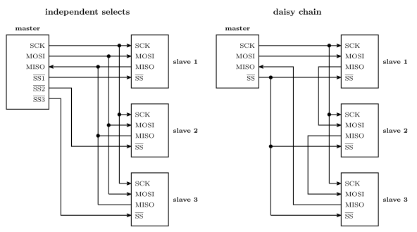
Figure 2: Two ways to give one SPI master three slaves. Left, independent selects: SCK and MOSI go to every slave, every slave’s MISO joins the one wire back to the master, and each slave has a select line of its own. The master pulls one select low at a time, and a slave that is not selected lets go of MISO, which is what lets them share it. Right, a daisy chain: one select line goes to all three, and the data goes through them in turn, from the master’s MOSI into slave 1, out of each slave’s MISO into the next one’s MOSI, and from the last slave’s MISO back to the master. A dot is a connection; lines that cross without a dot are not connected.
Independent selects. SCK and MOSI go to every slave, and all the slaves’ MISO pins share the one wire back. Each slave gets its own select line, \(\overline{\text{SS1}}\), \(\overline{\text{SS2}}\), \(\overline{\text{SS3}}\), and the master pulls exactly one of them low for a transfer. An unselected slave ignores the clock and lets go of MISO, so only the selected one drives it. Each extra slave costs the master one more pin.
Daisy chain. One select line for all of them, and the data passes through each slave on its way round: master MOSI to slave 1, each slave’s MISO to the next slave’s MOSI, the last slave’s MISO back to the master’s MISO. The registers now make one long ring, 8 bits for the master and 8 more for each slave. It needs no extra pins however many slaves there are, but every transfer goes through all of them.
Worked: loading a daisy chain
Three slaves are daisy-chained and the master wants 0xA1 in slave 3, 0xB2 in slave 2 and 0xC3 in slave 1. In what order does it send the bytes, for how many clocks, and what comes back?
Each byte sent pushes every byte already in the chain one slave further along, so the byte meant for the farthest slave has to go first: 0xA1, then 0xB2, then 0xC3, with \(\overline{\text{SS}}\) held low for all 24 clocks. After the first 8, 0xA1 is in slave 1; the next 8 push it to slave 2 and put 0xB2 in slave 1; the last 8 push it to slave 3. What comes back to the master is what the slaves held before, the farthest slave’s old byte first: if they held 0x11, 0x22 and 0x33, the master receives 0x33, 0x22, 0x11. The step-by-step picture is in avr-spi.
SPI on the ATmega324A
- The ATmega324A has one SPI port.
- It shares pins with the upper half of port B: PB4 is \(\overline{\text{SS}}\), PB5 is MOSI, PB6 is MISO and PB7 is SCK.
- The hardware generates the signals. The program writes one byte; the port makes the eight clock pulses and does the shifting by itself.
- It can be a master or a slave, chosen by a bit in its control register.
- The datasheet covers it on pages 166 to 174.
- The USARTs can also be used as SPI masters, which gives the chip up to three (avr-spi).
Inside the chip the SPI block is wired to port B, the TWI block to port C, and the two USARTs to port D, apart from USART0’s clock pin on port B (the chip’s other blocks are in avr-architecture). The pins are:
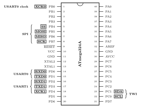
Figure 3: The ATmega324A’s 40 pins, with the serial interfaces marked. Each pin is named for its port bit, and the boxed names are the alternate uses that matter here. The SPI port is the upper half of port B, PB4 to PB7. The TWI is PC0 and PC1. USART0 receives and transmits on PD0 and PD1, and USART1 on PD2 and PD3; XCK0 and XCK1 are the USARTs’ clock pins, which is where the clock comes out when a USART works as an SPI master. Whichever interface is switched on takes its pins over from the port.
The datasheet’s pinout is shared with bigger chips in the same family, and some pins also list functions of a fourth timer (T3, ICP3, OC3A, OC3B) that the ATmega324A does not have, just as its block diagram shows a 16-bit T/C 3 (2026-08-27-avr-introduction).
The SPI clock rate
As a master, the AVR makes SCK by dividing its own clock, and the divider can be chosen. With the 8 MHz clock:
| Divider | SCK |
|---|---|
| 2 | 4 MHz |
| 4 | 2 MHz |
| 8 | 1 MHz |
| 16 | 500 kHz |
| 32 | 250 kHz |
| 64 | 125 kHz |
| 128 | 62.5 kHz |
As a slave, the fastest SCK it can follow is \(f_{OSC}/4\), 2 MHz at 8 MHz. A slave does not run its SPI logic from SCK directly. It samples the incoming SCK with its own clock, and each high and each low half of SCK has to last a couple of its own clock cycles to be seen reliably. Which bits choose the divider is in avr-spi.
Worked: how long does a byte take?
A byte is 8 SCK periods, and each period is divider CPU clock cycles.
| Divider | CPU cycles per byte | Time per byte at 8 MHz |
|---|---|---|
| 2 | \(8 \times 2 = 16\) | 2 µs |
| 16 | \(8 \times 16 = 128\) | 16 µs |
| 128 | \(8 \times 128 = 1024\) | 128 µs |
For comparison, one 8N1 UART frame at 9600 baud takes \(10 / 9600 \approx 1.04\) ms, about 500 times as long as an SPI byte at the fastest rate.
Worked: two AVRs
Two ATmega324As, both on 8 MHz clocks, are joined by SPI. What is the fastest master setting that works? The slave can follow at most \(8\text{ MHz}/4 = 2\) MHz, so the master’s divider must be 4 or more. Divider 2 gives 4 MHz, which a master can produce but this slave cannot follow.
Bit bashing
Sometimes a microcontroller has no hardware support for a bus standard, or not enough interfaces of that standard: a second SPI bus wanted on a chip with one SPI port, say. The standard can then be simulated with general purpose port pins. The program drives each output pin and reads each input pin itself, one edge at a time, in the order the standard lays down. This is bit bashing, also called bit banging.
For an SPI master, each of the eight bits is four steps on ordinary pins: put the next bit on the MOSI pin, raise the SCK pin, read the MISO pin, lower the SCK pin. The code, and what it costs, are in serial-communication.
Bit bashing suits a synchronous standard well. The master makes the clock, so if the program is held up between two edges, by an interrupt for instance, the transfer just pauses and nothing goes wrong. An asynchronous standard such as a UART has no clock to wait for, so a bit-bashed UART has to time every bit exactly.
Worked: one SPI port, two SPI buses
A design on the ATmega324A needs to be the master on two separate SPI buses, and the SPI port is already in use for one of them. What are the options for the other?
- A USART in master SPI mode. Hardware does the shifting, as with the SPI port, on the USART’s XCK, TXD and RXD pins (avr-spi).
- Bit bashing on any three spare port pins, plus one for the select. It works anywhere, but the CPU does all of the work and the bus runs much slower.
If the second “bus” is really just more slaves, neither is needed: one SPI port drives several slaves through separate select lines.
AVR I/O coding
Volatile variables
volatile int running;volatile tells the compiler that the variable can change outside the standard flow of control: in an interrupt handler, or in another thread. The compiler must then not apply the optimisations that assume only the code in front of it changes the variable. Every read in the source becomes a real read of memory, and every write a real write.
Worked: a loop that never ends
A button on INT0 is meant to start the program running:
volatile int running;

ISR(INT0_vect) {
    running = 1;              /* the button has been pushed */
}

int main(void) {
    /* ... set up INT0 for the button, then sei() ... */
    running = 0;
    while (!running) {
        ;                     /* do nothing until the button is pushed */
    }
    /* carry on */
}
What does an optimising compiler do with the loop if running is declared without volatile?
It changes the loop to
while (1) {
    ;
}
The compiler looks at main on its own. It has just set running to 0, and nothing inside the loop writes running, so as far as it can tell !running is true every time and testing it again is wasted work. The handler is a separate function that main never calls, so its write is invisible to that reasoning. The result is a program that never leaves the loop, however often the button is pushed. With volatile, each test of !running reads the variable from memory, and the first test after the handler has run sees 1 and the loop ends.
The register names PINC, PORTA and the rest are volatile for the same reason: a pin can change without the program changing it (c-preprocessor-and-avr-headers). On this 8-bit CPU a one-byte uint8_t is a better type for a flag than int, because it is read in a single instruction and an interrupt cannot land halfway through (avr-interrupts). The two-column picture of what volatile changes is in 2026-09-21-interrupts.
Setting I/O register bits
When setting or clearing particular bits of an I/O register, be explicit about which bits. These three lines all have the same effect:
| Code | What the reader has to do | |
|---|---|---|
| Poor | TCCR1B = 10; |
convert 10 to binary, then look up what each 1 is |
| Better | TCCR1B = 0x0A; |
read the bits off the hex, then look them up |
| Best | TCCR1B = (1<<WGM12)\|(1<<CS11); |
nothing: the two bits being set are named |
Worked: are they really the same?
\(10 = 8 + 2\), which is 0000 1010, which is 0x0A. In TCCR1B, WGM12 is bit 3 and CS11 is bit 1, so
\[(1 \ll 3)\ |\ (1 \ll 1) = \texttt{0000 1000}\ |\ \texttt{0000 0010} = \texttt{0000 1010}\]
All three are the same byte, and since the compiler works out (1<<WGM12)|(1<<CS11) while compiling, all three produce the same machine code. The readable form costs nothing.
And what does it do? WGM12 = 1, with WGM13 cleared by the same write and WGM11:10 left at 0 in TCCR1A, makes WGM13:0 = 0100: CTC mode with the top of the count in OCR1A. CS12:0 = 010 divides the clock by 8. It is the set-up for the 10 ms tick in week9-lab-avr-interrupts (avr-timers-and-counters). The best form says so to anyone who knows the bit names. The poor form says nothing.
Where the names come from
The register and bit names are the datasheet’s. Each register is drawn in its section of the datasheet with its address and its bits. The datasheet has errors in places, so check a name against the I/O register summary at the back before trusting it. The SPI port is a case in point: its own chapter calls the enable bit SPE and the master bit MSTR, but the names that compile are SPE0 and MSTR0, which is how the summary writes them (avr-spi). For timer/counter 0’s TCCR0B, on page 112:
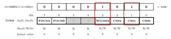
Figure 4: Timer/counter 0’s control register B in the datasheet’s three-row form: bit numbers above, names in the boxes, then whether each bit can be read or written and its value after reset. The register is I/O register 0x25, data address 0x45. Bits 5 and 4, shaded grey, are unused and read as 0; the two FOC bits can only be written. Each bit name is defined in the device header as its bit number, so WGM02 is 3 and CS01 is 1, and shifting 1 left by that number puts a 1 in the named column. The two outlined columns follow each name up through its bit number to its 1 in the top row: ORed together, (1<<WGM02)|(1<<CS01) is 0000 1010, which is 0x0A.
Bit names are macros, defined in the device header that <avr/io.h> pulls in:
#define WGM02 3A bit name is the bit’s number, not its mask. That is why it is always written (1<<WGM02): the shift turns the number 3 into the mask 0000 1000.
The same names work in assembly, where the assembler works out the expression:
ldi r16, (1<<WGM02)|(1<<CS01)Worked: what does that load?
WGM02 is 3 and CS01 is 1, so the constant is 0000 1000 | 0000 0010 = 0x0A, and the instruction in flash is simply ldi r16, 0x0A. To put it in the register takes out TCCR0B, r16, which works because TCCR0B is I/O register 0x25, inside the 64 that out can reach (avr-io-ports).
It is the same byte as TCCR1B = 0x0A above, and it shows why the names matter. In TCCR1B, bit 3 is WGM12, one bit of timer 1’s four-bit mode, and 0x0A gives CTC. In TCCR0B, bit 3 is WGM02, the top bit of timer 0’s three-bit mode, and with TCCR0A’s two mode bits at 0 it makes the mode 100, which is reserved: no use at all. Timer 0’s CTC mode is WGM01, in TCCR0A. A bit name means something only in its own register, and (1<<WGM12) written into TCCR0B would quietly set WGM02, because both are bit 3.
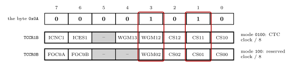
Figure 5: One byte, two registers, two meanings. The byte 0x0A has its 1s in bits 3 and 1, outlined. In TCCR1B those bits are WGM12 and CS11; in TCCR0B the same positions are WGM02 and CS01, because bit names are only bit numbers. The clock select field lines up in both, so the clock is divided by 8 either way. The mode does not: with the mode bits in TCCR1A and TCCR0A left at 0, bit 3 makes timer 1’s four-bit mode 0100, CTC, and timer 0’s three-bit mode 100, a reserved code that should not be used. Unused bits are shaded grey.
Clearing and toggling I/O register bits
The same rules apply: name the bit, and change only that bit.
PORTC &= ~(1<<5);         /* clear bit 5 of port C's output: PC5 driven low   */
TIMSK2 ^= (1<<OCIE2A); /* toggle the timer 2 output compare A interrupt enable */- To clear a bit, AND with a mask that has a 0 on that bit and 1s everywhere else.
~(1<<5)is the complement of0010 0000, which is1101 1111. ANDing with 1 keeps a bit and ANDing with 0 clears it. - To toggle a bit, XOR with a mask that has a 1 on that bit.
OCIE2Ais bit 1 ofTIMSK2, so the mask is0000 0010. XOR with 1 flips a bit and XOR with 0 keeps it. - To set a bit, OR with a 1 on it, as above.
Each of these reads the register, changes one bit and writes it back, leaving the other seven alone. Set, clear and toggle side by side on one byte are drawn in bit-masking.
Worked: clear bit 5 of port C
Which register does the clear go to?
PORTC, the register that holds the values port C drives: PORTC &= ~(1<<5); makes PC5 go low and leaves the other seven outputs as they were. Not PINC. PINC holds the levels on the pins, it is not a store, and on this chip writing a 1 to a bit of PINC toggles the matching bit of PORTC. PINC &= ~(1<<5) reads the pins, clears bit 5 of that reading and writes it back, which flips every other output that happened to read high and leaves PC5 alone: the opposite of what was wanted. The details are in avr-io-ports.
Worked: does this line enable the interrupt?
/* enable output compare A interrupt for timer 2 */
TIMSK2 ^= (1<<OCIE2A);
Only if it was off. XOR flips the bit. If OCIE2A was 0 this sets it and the interrupt is enabled; if it was already 1, the same line clears it and disables the interrupt. Run twice, it undoes itself. To enable, whatever the bit was before, set it:
TIMSK2 |= (1<<OCIE2A);    /* enable  */
TIMSK2 &= ~(1<<OCIE2A);   /* disable */
Toggling is for things that are meant to alternate, like blinking an LED with PORTC ^= (1<<0); from a timer handler.
See also
- serial-communication — masters and slaves, I²C with its pull-ups, SPI next to the UART, bit bashing in code
- avr-spi — the SPI port in full: the exchange clock by clock, timing, several slaves, the registers, the clock rate bits, code
- bit-masking — set, clear and toggle as bitwise operations, and writing registers by bit name
- avr-io-ports — changing one bit of a port, writing to
PINx, the pins’ alternate functions - avr-interrupts · 2026-09-21-interrupts —
volatileand interrupt handlers - c-preprocessor-and-avr-headers — where the register and bit names are defined
- avr-timers-and-counters — the fields of
TCCR0BandTCCR1B - shift-registers — the heart of SPI
- week10-lab-adc-and-spi — Lab 16, the SPI port driving an LED matrix
- 2026-09-24-serial-io — Lecture 18 · 2026-10-08-assembly-process — Lecture 20
Lecture 20 — Assembly Process
Assembly language is more than instructions, and turning it into machine code takes more than translating one line at a time. This covers the four fields of a statement, the directives that speak to the assembler instead of the CPU, the AVR’s three memory segments, and the two-pass assembler that gets round the forward reference problem. Two programs are traced to find the address every label is given. The reference note is assembly-process. The program skeleton it all fits into is avr-program-structure, and the memories behind the segments are in memory-models.
Goals
- See that an assembly program holds more than instructions: directives tell the assembler where things go and what names mean.
- Know the AVR’s memory segments and which directives put what in each.
- Understand how an assembly program becomes machine code, and why the assembler reads the source twice.
- Be able to work out by hand the address each label is given.
Where assembly sits
The six levels of a computer are in 2026-07-27-course-intro-bits-bytes-binary. There are two roads down to machine code:
- a C program, at the problem-oriented language level, is compiled, and one line can become many instructions (2026-09-07-introduction-to-embedded-c-programming; the rest of that road is 2026-10-15-compilation-and-linking);
- an assembly program, one level down, is assembled, each instruction to exactly one machine instruction.
Each instruction on its own has a fixed binary form, its machine code (avr-instructions). That leaves two questions: what else goes in an assembly program, and how does the assembler turn a whole program into machine code?
The four fields of a statement
A statement has four parts, called fields:
formula: ldi r20, i ; register r20 = i| Field | Here | What it is |
|---|---|---|
| label | formula: |
a name for the address this statement lands at |
| operation (opcode) | ldi |
the mnemonic |
| operand(s) | r20, i |
what the operation works on |
| comment | ; register r20 = i |
explanation, ignored by the assembler |
The fields are drawn one by one in assembly-process.
- Labels are needed so that statements can be jumped to, and so that data can be referred to. The label’s value is an address:
formulais the address of thatldi. A label usually starts in column 1, with everything else indented. - The operation is a symbolic abbreviation for the opcode, for example
LDS, Load Direct from data Space. - The operand field gives the addresses and registers the instruction uses. Register names vary from machine to machine: the Pentium has
eax,ebx,esi,ediand so on; SPARC haso0..o7,i0..i7,l0..l7andg0..g7; the AVR simply hasr0..r31. - The comment is for people only, and in assembly it is vital: the instructions say what happens, never why.
- Some assemblers require a semicolon to end each statement and some do not. The AVR’s does not, and there a semicolon begins a comment.
Directives
The assembler needs information that is not an instruction:
- where in memory the program and its data should go;
- nicer names to use for registers and addresses, such as
temporSPH.
That information is a command to the assembler itself, a pseudo-instruction or directive. Directives are preceded by a dot: .byte reserves space for a variable, and .def temp = r16 lets the program say temp for register r16.
Memory segments
To the assembler, the different types of memory are segments, and directives choose which segment code and data go into. The AVR has three:
| Segment | Directive | Memory | What goes there |
|---|---|---|---|
| data | .dseg |
RAM (SRAM) | nothing can be placed: only space reserved, for variables |
| code | .cseg |
flash | program code or constant data |
| EEPROM | .eseg |
EEPROM | constants |
One source file can switch between segments as often as it likes. Each piece goes to its own memory, and pieces of the same segment are joined end to end, as Figure 6 below shows for data and assembly-process shows for all three.
The directives
The assembler in Microchip Studio (formerly Atmel Studio) is AVRASM2. It has these directives, among others:
| Kind | Directives |
|---|---|
| choosing a segment | .cseg code, .dseg data, .eseg EEPROM; .csegsize sets the program memory size |
| reserving and defining data | .byte reserves bytes for a variable; .db defines constant bytes; .dw defines constant words |
| naming | .def gives a register a symbolic name; .equ sets a symbol to an expression; .set does the same but can be changed |
| placing | .org sets the program origin, the location counter |
| files | .include reads source from another file; .exit stops reading this one |
| list file | .list and .nolist turn list-file generation on and off; .listmac shows macro expansions in it |
| macros | .macro begins one; .endm or .endmacro ends it |
| conditional assembly | .if opens a block that is assembled only when its condition holds; .else, .elif and .endif continue and close it |
Each is described in assembly-process.
Reserving space and defining constants
.byte reserves space, and it is allowed only in the data segment.
.cseg and .dseg let the code and data segments be built up in pieces: switching back to a segment carries on where it left off.
Worked: a data segment built in pieces
Where do amount and count go?
        .dseg
amount: .byte 2
        .cseg
formula: ...
        .dseg
count:  .byte 2
The data counter starts at 0x0100 (256), the first SRAM address after the 32 registers, the 64 I/O registers and the 160 extended I/O registers.
.dseg: use the data counter, at0x0100.amount=0x0100..byte 2reserves0x0100and0x0101; the counter moves to0x0102..cseg:formulaand whatever follows it go to program memory, under the code counter. The data counter is left alone at0x0102..dseg: back to the data counter, still0x0102.count=0x0102(258). It reserves0x0102and0x0103, and the counter ends at0x0104.
So count sits immediately after amount in SRAM, although the code for formula lies between them in the file.
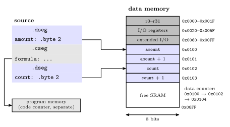
Figure 6: A data segment built in two pieces. The data counter starts at 0x0100, just past the registers and the I/O registers, so amount gets the two bytes there. The code in the middle of the file goes to program memory under the code counter and does not move the data counter, so when the file returns to the data segment count takes the next two bytes, 0x0102 and 0x0103. Nothing is written into these bytes: the assembler only gives out addresses, and the rest of SRAM up to 0x08FF stays free. Blue marks the data segment and grey the code segment.
.db initialises constants in the code or EEPROM segment, 8 bits each. .dw does the same with 16-bit words. Program memory is 16 bits wide, so .db bytes go two to a word, and an odd count is padded with a zero byte.
Worked: a lookup table
Where do the three tables go, and what is in each word?
        .cseg
table1: .db  11, 12, 30
table2: .dw  100, 133
        .org 500
table3: .dw  ...
With the code counter at 0:
table1= 0. Word 0 holds 11 and 12; word 1 holds 30 and a pad 0. The counter moves to 2. Writing the pad as a fourth value,.db 11, 12, 30, 0, gives exactly the same two words, without the assembler’s padding warning.table2= 2. Word 2 is 100 and word 3 is 133. The counter moves to 4..org 500sets the counter to 500, skipping words 4 to 499.table3= 500.
The layout is drawn in assembly-process.
Registers, devices and files
.defmakes a definition, for registers only:.def ZH=r31 .def ZL=r30.devicesays exactly which processor the program is for, as in.device ATmega324A. The assembler then refuses any instruction that chip does not implement..includeincludes another file at that point, as.include "m324Adef.inc"does in every program so far (avr-program-structure)..exitstops processing the file.
Symbols and the location counter
.equequates a symbol to a value, and the value cannot be changed..setequates too, but the value can be changed by a later.set..equ sreg = 0x3f ; Status register .set io_offset = 0x23 ; For nowsregis fixed for the whole file.io_offsetis 0x23 for now: a later.set io_offset = ...replaces it from that line on..orgsets the location counter, the address the next item will be placed at, in whichever segment is current.
All of these are the syntax of the assembler built into Microchip Studio. Other assemblers, even ones for the AVR, use different syntax: avr-gcc’s assembler reads .byte as “store these bytes”, not “reserve this many”.
The forward reference problem
An assembly program is a sequence of one-line statements, but the assembler cannot always read a statement and produce its machine code on the spot. add r1, r2 is fine: the opcode and both registers are known, so the word can be written immediately. A program’s first statement is usually
jmp RESETand the RESET: label is further down. At the jmp, the assembler knows the opcode but not the operand: it has no address for RESET, so it cannot generate the instruction. This is the forward reference problem.
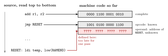
Figure 7: Why a single pass from top to bottom is not enough. The add names only registers, so its machine word is complete the moment the line is read. The jmp is two words: the first holds the opcode and can be written, but the second must hold the address of RESET, and RESET is defined further down. By the time the assembler reaches that definition and learns the address, the jmp is already behind it. Red marks the word that cannot be filled in yet and the line that supplies its value.
Two passes
The solution is to process the file twice.
- Pass one defines all the symbols: labels, and the names made by
.equ,.setand.def. It keeps a location counter for each segment and records every symbol’s value in a symbol table. It does not need any operand to do this, only each statement’s size. - Pass two starts again from the top. The values of all the symbols are now known, so it can assemble each instruction, which means producing the actual machine code.
The pipeline is drawn in assembly-process.
Worked: the two-pass example
At what program address will the instruction at label RESET be placed, and what are the other symbols’ values?
        .equ    RAMEND = $08FF
        .equ    SPH = $3E
        .equ    SPL = $3D
        .def    ZH = r31
        .def    ZL = r30
        jmp     RESET
        .dseg
var1:   .byte   2
var2:   .byte   2
        .cseg
        .def    temp = r16
mesg:   .db     72,101,108,108,111
table:  .dw     var1, var2
RESET:  ldi     temp, low(RAMEND)
        out     SPL, temp
        ldi     temp, high(RAMEND)
        out     SPH, temp
        ...
        ldi     ZH, high(mesg*2)
        ldi     ZL, low(mesg*2)
        lpm                     ;R0 <= M[Z]
Pass one, one line at a time. Code counter from 0 (in words), data counter from 256, 0x0100 (in bytes), EEPROM counter not used.
| Line | Segment | Placed at | Size | Counter after | Symbol table gains |
|---|---|---|---|---|---|
.equ RAMEND = $08FF |
0 | RAMEND = 0x08FF |
|||
.equ SPH = $3E |
0 | SPH = 0x3E |
|||
.equ SPL = $3D |
0 | SPL = 0x3D |
|||
.def ZH = r31 |
0 | ZH = r31 |
|||
.def ZL = r30 |
0 | ZL = r30 |
|||
jmp RESET |
code | 0, 1 | 2 words | code 2 | |
.dseg |
data | 0 | data 256 | ||
var1: .byte 2 |
data | 256, 257 | 2 bytes | data 258 | var1 = 256 |
var2: .byte 2 |
data | 258, 259 | 2 bytes | data 260 | var2 = 258 |
.cseg |
code | 0 | code 2 | ||
.def temp = r16 |
0 | temp = r16 |
|||
mesg: .db 72,101,108,108,111 |
code | 2, 3, 4 | 5 bytes + pad = 3 words | code 5 | mesg = 2 |
table: .dw var1, var2 |
code | 5, 6 | 2 words | code 7 | table = 5 |
RESET: ldi temp, low(RAMEND) |
code | 7 | 1 word | code 8 | RESET = 7 |
out SPL, temp |
code | 8 | 1 word | code 9 | |
ldi temp, high(RAMEND) |
code | 9 | 1 word | code 10 | |
out SPH, temp |
code | 10 | 1 word | code 11 |
The data counter runs 256, 258, 260, and the code counter 0, 2, 5, 7 and on.
The instruction at RESET is at program address 7. The full table, and the trace drawn line by line, are in assembly-process.
| Symbol | Segment | Value |
|---|---|---|
RAMEND |
0x08FF |
|
SPH |
0x3E |
|
SPL |
0x3D |
|
ZH |
r31 |
|
ZL |
r30 |
|
RESET |
code | 7 |
var1 |
data | 256 |
var2 |
data | 258 |
temp |
r16 |
|
mesg |
code | 2 |
table |
code | 5 |
RESET can go in the table the moment the jmp mentions it, with its value left blank until RESET: turns up; the finished table is the same either way.
Pass two fills in every operand:
jmp RESETbecomesjmp 7, two words0x940C 0x0007..dw var1, var2writes the two data addresses, 256 and 258 (0x0100and0x0102), into words 5 and 6.ldi temp, low(RAMEND)becomesldi r16, 0xFFandldi temp, high(RAMEND)becomesldi r16, 0x08. With the twoouts toSPLandSPH(I/O addresses0x3Dand0x3E), they set the stack pointer to the top of SRAM (procedures-and-the-stack).mesg*2= 4, soldi ZH, high(mesg*2)loads 0 andldi ZL, low(mesg*2)loads 4.mesgis word 2, which starts at byte 4, andlpmwants a byte address in Z. It loadsr0with the byte there: 72, theHofHello(memory-models).
Every encoded word is listed in assembly-process.
Worked: where does RESET land?
At what program address will the instruction at label RESET be placed?
        jmp RESET
        jmp ISR1
        jmp ISR2
.dseg
var1: .BYTE 1
var2: .BYTE 3
var3: .BYTE 2
.cseg
.def temp=r20
message1: .DB 72,101,111,111,0
message2: .DB 0,65,66,68,0
RESET:
        ldi temp, low(RAMEND)
        out SPL, temp
        ldi temp, high(RAMEND)
out SPH, temp- A. 9
- B. 12
- C. 15
- D. 18
- E. None of the above
B, 12. Follow the code counter only:
- Three
jmps at 2 words each: addresses 0, 2 and 4. The counter is at 6. - The
.dsegblock moves the data counter:var1=0x0100,var2=0x0101,var3=0x0104, ending at0x0106. The code counter does not move. .csegreturns to the code counter, still 6..deftakes no space.message1: 5 bytes, padded to 6, is 3 words: 6, 7 and 8. The counter is at 9.message2: another 5 bytes, padded to 6, so 3 words: 9, 10 and 11. The counter is at 12.RESET:labels the next instruction: 12.
\[\underbrace{3 \times 2}_{\texttt{jmp}} + \underbrace{3}_{\texttt{message1}} + \underbrace{3}_{\texttt{message2}} = 12\]
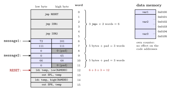
Figure 8: Program memory for the question, one 16-bit word per row, lowest address at the top. Each jmp takes two words, the opcode and the target address. Each .DB line of five bytes fills two and a half words, and the assembler pads the last half with a zero so the next line starts on a whole word. That puts message1 at 6, message2 at 9 and RESET at 12. The variables are in data memory under their own counter, so they take no program memory at all. Light grey marks instructions, blue the .DB bytes and the variables, and dark grey the pad bytes.
Each wrong answer matches a slip worth recognising:
- A, 9, counts each
jmpas one word: \(3 + 3 + 3\). - C, 15, lets the six bytes of variables into the code counter as three words: \(6 + 3 + 3 + 3\). The
.dseglines have their own counter and take no program memory. - D, 18, makes the same mistake with the six bytes as six words, \(6 + 6 + 3 + 3\), or gives every
.DBbyte a word of its own, \(6 + 6 + 6\) with the pads. - E would be right if the two strings were packed together with no padding between them, \(6 + 5 = 11\). The assembler pads each
.DBline separately.
See also
- assembly-process — the reference note: statement fields, every directive, segments and location counters, the two-pass assembler with figures, and the encoded output of the example
- avr-program-structure — the program skeleton, now with its directives and segments
- memory-models — word addresses against byte addresses, and the AVR’s separate address spaces
- avr-branches-and-jumps — why
jmpis two words andrjmpone - avr-interrupts — the vector table that the three
jmps at the top belong to - procedures-and-the-stack — the stack-pointer set-up after
RESET: - 2026-10-05-more-io — Lecture 19
- 2026-10-15-compilation-and-linking — Lecture 22: the road from C
Lab 16 — A/D and SPI
Learning Lab 16: two more of the ATmega324A’s peripherals, each with a device to drive. The analog to digital converter reads a joystick, and the SPI port sends commands to an LED matrix. Five tasks build from wiring the joystick up to an Etch-A-Sketch that draws on the matrix with it. The converter is in analog-to-digital-conversion, the SPI bus in avr-spi, the joystick and the LED matrix in io-board, and the timer used to pace the programs in avr-timers-and-counters. The lectures behind it are 2026-09-24-serial-io (Lecture 18) and 2026-10-05-more-io (Lecture 19).
Outline
- The A/D converter, used to read the joystick
- SPI, used to drive the LED matrix
- One timer question, about a slow count for pacing a program
- Five tasks, worked in full at the end
The A/D converter
The facts the lab relies on (analog-to-digital-conversion):
- The port A pins can be used as analog inputs.
- There is one converter, behind an analog multiplexer, so one input is converted at a time.
- The reference voltage can be chosen. The lab uses the supply, \(V_{cc} = 5\ \text{V}\), which reaches the converter as AVCC.
- The resolution is 10 bits: results from 0 to 1023.
- A conversion takes time: up to 3200 clock cycles, 0.4 ms at 8 MHz. The converter runs on its own clock, and a conversion takes 13 of its cycles, 25 for the first one after it is switched on. At the slowest setting, the clock divided by 128, that first conversion is \(25 \times 128 = 3200\) cycles. A faster converter clock gives a quicker answer with fewer accurate bits.
- So the program has to find out when a conversion has finished, either by polling the start bit
ADSC, which reads 1 until the result is ready, or by taking the interrupt at the end of the conversion (polling-and-interrupts).
Worked: the ADC clock prescaler
The ADC clock needs to run between 50 kHz and 200 kHz for full precision. What are the bounds for the ADC clock prescaler?
A. 80 to 320 · B. 40 to 160 · C. 20 to 80 · D. 25 to 100 · E. 50 to 150 · F. 160 to 640 · G. 30 to 120 · H. 10 to 40
B. The ADC clock is the 8 MHz system clock divided by the prescaler \(N\), so
\[50\ \text{kHz} \le \frac{8\ \text{MHz}}{N} \le 200\ \text{kHz} \quad\Longleftrightarrow\quad \frac{8\ \text{MHz}}{200\ \text{kHz}} \le N \le \frac{8\ \text{MHz}}{50\ \text{kHz}} \quad\Longleftrightarrow\quad 40 \le N \le 160.\]
A bigger divisor gives a slower clock, so the upper frequency limit sets the lower bound on \(N\). The bounds are in the ratio 4 to 1 because the frequencies are, and most of the other options have that ratio too: A, C, D, F, G and H are the right answers for system clocks of 16, 4, 5, 32, 6 and 2 MHz. E, 50 to 150, is not in the ratio 4 to 1 and is right for no clock.
The prescaler only offers powers of two, 2 to 128, so two settings land in the window: 64, giving 125 kHz, and 128, giving 62.5 kHz. The programs below use 64, which puts the clock in the middle of the window and makes a conversion \(13 \times 64 = 832\) cycles, 104 µs.
Worked: the ADMUX value
What value needs to go in ADMUX to use AVCC as the reference voltage, right adjust the result and select input ADC1?
ADMUX holds three fields (analog-to-digital-conversion):
| Field | Bits | Wanted | Value |
|---|---|---|---|
REFS1:0, reference |
7, 6 | AVCC | 01 |
ADLAR, adjust |
5 | right adjusted | 0 |
MUX4:0, input |
4 to 0 | ADC1 on its own | 00001 |
Put together, 0100 0001, which is 0x41. In C, ADMUX = (1<<REFS0) | 1;, or (1<<REFS0) | (1<<MUX0).

Figure 9: The value 0x41 in ADMUX, bit by bit. The top two bits choose the reference voltage, and 01 means AVCC, the 5 V supply. Bit 5 chooses how the 10-bit result sits in its 16-bit register, and 0 means right adjusted, so it reads as a number from 0 to 1023. The bottom five bits choose the input, and 00001 is ADC1, pin PA1. The two shaded bits are the ones set.
The joystick
The joystick is a small board made to sit in the breadboard. Each axis is a potentiometer between its own supply pin and ground, and the stick moves the wiper, so each axis gives a voltage between 0 and 5 V (io-board):
| Pin | Connect to | What it is |
|---|---|---|
| L/R+ and U/D+ | VCC, 5 V, both of them | the top end of each potentiometer |
| GND (two of them) | GND, one is enough | the bottom end of both |
| L/R (two of them) | an analog input | x: 0 V with the stick to the left, 5 V to the right |
| U/D (two of them) | an analog input | y: 0 V at the bottom, 5 V at the top |
The pins come in pairs that are joined on the board, so only one L/R, one U/D and one GND need a wire. The two + pins are not joined to each other, so both need one.
Where it goes. At the right-hand end of the breadboard, leaving room for the microcontroller board and its programmer to the left. Turned the right way, the X arrow printed on the board points to the top of the breadboard. So the stick’s own left and right, the direction x measures, run along the breadboard from bottom to top, and its up and down run from right to left. The board’s pins are protected by a piece of black foam when it is not in use, which is worth keeping.
The programs below use PA0 (ADC0) for x and PA1 (ADC1) for y.
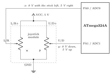
Figure 10: The joystick wired to the microcontroller. Each axis is a potentiometer from its own supply pin down to ground, and the stick sets the wiper, so the wiper voltage goes from 0 V to 5 V as the stick crosses from one side to the other. The two supply pins, L/R+ and U/D+, are separate and both go to VCC. The x output goes to PA0, which is analog input ADC0, and the y output to PA1, ADC1. The module’s second L/R, U/D and GND pins are joined to these inside it and are left unconnected.
Worked: the stick pulled down
The joystick is seen from above, turned a quarter turn clockwise from the way it sits in the breadboard, so that its L/R+ and U/D+ pins are at the top corners and its two GND pins at the bottom corners. That puts its own x axis across and its y axis up. The stick is pulled straight towards the bottom edge. What (x, y) should the ADC read?
A. (−511, 0) · B. (−511, 511) · C. (−511, 1023) · D. (0, −511) · E. (0, 511) · F. (0, 1023) · G. (511, −511) · H. (511, 0) · I. (1023, −511) · J. (1023, 0)
H, (511, 0). Straight down leaves x where it rests, in the middle, and takes y as low as it goes.
- x is in the middle of its range. The wiper sits halfway, 2.5 V, and halfway through 0 to 1023 is 511.5. A reading of 511 or 512 both mean centred.
- y is at the bottom of its range, 0 V, which reads 0.
- No reading is negative. The converter’s result is an unsigned number from 0 to 1023, so every option with \(-511\) in it is out. Those are what a reading measured from the centre would look like, which a program can work out by subtracting 511, but the converter itself never reports.
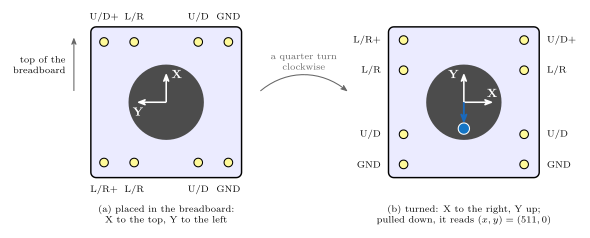
Figure 11: Why the stick’s x runs across and its y runs up in this view. The X and Y arrows printed under the stick mark the directions in which L/R and U/D rise from 0 V to 5 V. Placed in the breadboard (a), X points to the top of the breadboard and Y to the left. A quarter turn clockwise (b) puts L/R+ and U/D+ at the top corners and the GND pins at the bottom corners, and turns X to point right and Y up, so the readings are laid out the usual way. The blue dot is the stick, pulled towards the bottom edge. That is at right angles to X, so x stays at the centre of its range, and straight against Y, so y is at its lowest.
It is “should”, not “will”. A real stick at rest sits a few counts away from 511, and when pulled all the way it may not quite reach 0 V. A program that tests for “centred” or “pushed down” needs a margin either side, as the programs below have.
Worked: where is (614, 689)?
The ADC is reading (x, y) = (614, 689). Where is the joystick? There are two parts to the answer, which way the stick is pushed and how far.
A. 15° anticlockwise of the right half-axis · B. 30° · C. 45° · D. 60° · E. 75°
F. 20 % tilted · G. 40 % tilted · H. 60 % tilted · I. 80 % tilted · J. 100 % tilted
D and G: 60° anticlockwise of the right half-axis, 40 % tilted. Measure from the centre, (511, 511):
\[\Delta x = 614 - 511 = 103, \qquad \Delta y = 689 - 511 = 178.\]
Both are positive, so the stick is up and to the right. Its direction, as an angle measured anticlockwise from straight right, is
\[\theta = \tan^{-1}\frac{\Delta y}{\Delta x} = \tan^{-1}\frac{178}{103} = \tan^{-1} 1.728 = 59.9^\circ \approx 60^\circ.\]
How far it is pushed is its distance from the centre, as a fraction of the 511 counts from the centre to full deflection:
\[\frac{\sqrt{103^2 + 178^2}}{511} = \frac{205.7}{511} = 0.40, \quad\text{so } 40\,\%.\]
Working backwards confirms it. Taking the exact centre, 511.5, full deflection is 511.5 counts, and 40 % of it is 204.6. At 60° that is \(204.6 \cos 60^\circ = 102.3\) across and \(204.6 \sin 60^\circ = 177.2\) up, which lands on (613.8, 688.7), and the converter reports whole numbers, (614, 689). Mixing up the axes gives 30°, since (689, 614) is the reading at 30°.
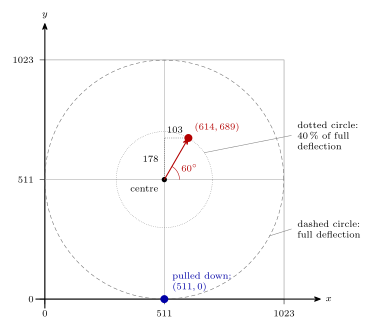
Figure 12: The joystick’s readings as a plane, x across and y up, each from 0 to 1023, with the centre at (511, 511). The dashed circle is full deflection, 511 counts from the centre. Pulling the stick straight down gives (511, 0): x stays centred and y goes to the bottom of its range. The reading (614, 689) is 103 counts right of the centre and 178 up. That is 206 counts from the centre, 40 % of full deflection, at 60° anticlockwise from the right half-axis. No reading is ever negative: the converter’s result runs from 0 to 1023.
SPI
SPI, the Serial Peripheral Interface, is the AVR’s synchronous serial port (avr-spi). The master and the slave each have an 8-bit shift register, and the two are joined in a ring: MOSI carries bits out of the master’s most significant end into the slave’s least significant end, and MISO carries bits out of the slave’s most significant end back into the master’s least significant end. The master makes the clock, SCK, and each pulse shifts both registers one place, so after eight pulses the two bytes have changed places. The slave takes part only while its select line, \(\overline{\text{SS}}\), is held low. With one master and one slave, the simplest arrangement holds the master’s own \(\overline{\text{SS}}\) high, so that it stays the master, and ties the slave’s low, so that it is always selected.
Sending a byte is writing it to the data register, and like a conversion it takes time: eight clock pulses. The program finds out it has finished by polling the flag SPIF0, or by taking the “serial transfer complete” interrupt, SPI_STC.
The names in code
The datasheet describes the SPI registers on pages 172 and 173 as SPCR and SPSR, but the ATmega324A header names them SPCR0 and SPSR0, with a 0 for SPI port 0. Their bit names take a 0 on the end as well: SPIE is SPIE0, SPE is SPE0, and SPR1 is SPR10. The data register follows the same pattern, SPDR0.
The datasheet’s register summary already has the 0s, with one slip: the bit printed there as SPR01 is SPR10.
Worked: master mode, slowest clock
Which bits of the SPI control registers SPCR and SPSR need to be set (1) to enable SPI in master mode with the slowest possible clock rate?
In SPCR0: SPE0, MSTR0, SPR10 and SPR00. In SPSR0: none. So SPCR0 = 0x53.
SPE0, bit 6 ofSPCR0, switches SPI on.MSTR0, bit 4, makes the AVR the master, the end that drives the clock.- The clock rate is set by three bits in two registers,
SPI2X0inSPSR0andSPR10:SPR00inSPCR0:
SPI2X0 |
SPR10 |
SPR00 |
SCK |
|---|---|---|---|
| 0 | 0 | 0 | clock / 4 |
| 0 | 0 | 1 | clock / 16 |
| 0 | 1 | 0 | clock / 64 |
| 0 | 1 | 1 | clock / 128 |
| 1 | 0 | 0 | clock / 2 |
| 1 | 0 | 1 | clock / 8 |
| 1 | 1 | 0 | clock / 32 |
| 1 | 1 | 1 | clock / 64 |
SPI2X0 doubles the speed, so the slowest rate has it at 0 and both SPR bits at 1: \(8\ \text{MHz} / 128 = 62.5\ \text{kHz}\). One byte then takes \(8 / 62\,500 = 128\ \text{µs}\).
The other bits stay 0: no interrupt (SPIE0), the most significant bit first (DORD0), and the clock idling low with data sampled on its rising edge (CPOL0, CPHA0). SPIF0 and WCOL0, the top two bits of SPSR0, are flags the hardware sets, not settings.
SPCR0 = (1<<SPE0) | (1<<MSTR0) | (1<<SPR10) | (1<<SPR00); /* 0x53 */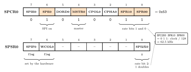
Figure 13: The two SPI registers set for master mode at the slowest clock. In SPCR0 the shaded bits are set: SPE0 turns SPI on, MSTR0 makes the AVR the master, and SPR10 and SPR00 select the slowest rate. The rate is the one setting split across two registers. Its third bit, SPI2X0, is bit 0 of SPSR0, and it stays 0, since setting it would double the speed. The top two bits of SPSR0 are status flags that the hardware sets.
The LED matrix
The LED matrix is 16 columns by 8 rows of pixels, each with a red and a green LED. It is an SPI slave: it takes commands, one byte at a time, from the AVR. It has two connection headers (io-board):
- K1, two pins, is its power. A two-wire lead joins it to the I/O board’s connector J1, VCC on the left pin and GND on the right.
- K2, four pins, is the SPI connection. It goes to the AVR’s SPI port, PB7 to PB4: SCK on PB7, MISO on PB6, MOSI on PB5 and \(\overline{\text{SS}}\) on PB4. The order of the four pins on K2 has to be matched against the pin names in the datasheet before the lead is plugged in.
The matrix’s reference manual describes everything it understands. The programs here use two commands, which are enough to draw anything.
The SPI pins are also the programming pins. The programmer loads the AVR’s flash through PB7 to PB5, so the matrix sees the programming traffic too, takes it for nonsense commands, and can end up showing Err. To clear it, hold the AVR’s reset button down for at least half a second after programming, then let the program start.
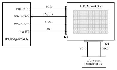
Figure 14: How the LED matrix is connected. Its SPI header K2 takes the four SPI pins of port B: the clock SCK, the data MOSI and the select line SS, which the AVR drives, and the data MISO coming back. Its power header K1 is fed from connector J1 on the I/O board, VCC on the left pin and GND on the right. The matrix only acts on bytes sent while SS is low.
The commands and the colour byte
Every message starts with a command byte. The two used here:
| Command | Bytes | Does |
|---|---|---|
| clear | 0x0F |
turns every pixel off |
| set one pixel | 0x01, position, colour |
sets the pixel at position to colour |
- The position byte is the row in the high nibble and the column in the low nibble:
(y << 4) | x, with x from 0 to 15 across and y from 0 to 7 up, (0, 0) being the bottom-left pixel. - The colour byte is the green brightness in the high nibble and the red brightness in the low nibble, each from 0 (off) to 15 (full):
(green << 4) | red. Mixing the two gives the colours between red and green.
| Colour byte | Green | Red | Colour |
|---|---|---|---|
0x00 |
0 | 0 | off (black) |
0x0F |
0 | 15 | red |
0x7F |
7 | 15 | orange |
0xFF |
15 | 15 | yellow |
0xF7 |
15 | 7 | chartreuse, a yellow-green |
0xF0 |
15 | 0 | green |
Worked: what colour is 0x7F?
What colour would a 0x7F colour data byte produce?
A. Red · B. Orange · C. Yellow · D. Chartreuse · E. Green · F. Black · G. Blue · H. Octarine
B, orange. 0x7F splits into a green nibble of 7 and a red nibble of 15: full red with about half as much green. Full red with full green, 0xFF, is yellow, so red with half the green sits between red and yellow, which is orange. Swapping the nibbles, 0xF7, gives chartreuse, the colour halfway from yellow to green. Blue is impossible on a matrix with only red and green LEDs, and octarine is a colour from fiction.
Worked: what do these bytes draw?
What would the LED matrix look like after receiving the bytes 0x0F, 0x01 0x24 0xF0, 0x01 0x46 0x0F? The six candidate pictures, A to F in Figure 15, each show one red and one green pixel, with each place given as (x, y): x across from the left and y up from the bottom, both counted from 0.
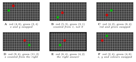
Figure 15: The six candidate pictures, each a 16 by 8 matrix with one red and one green pixel. E is what the bytes draw. Each of the others is the same two commands read with one slip, and the slip shows in where the pixels land. Reading the position byte’s nibbles the wrong way round swaps each pixel’s x and y (A). Counting x from the right mirrors the picture left to right (D). Counting from 1 instead of 0 moves every pixel one place down and one to the left (B). Reading the colour byte’s nibbles the wrong way round leaves the places alone but swaps the colours (C). F makes both swaps, A’s and C’s.
E. Split the bytes into commands:
0x0F: clear the display.0x01 0x24 0xF0: set one pixel. The position0x24is y = 2, x = 4, and the colour0xF0is green 15, red 0. Green at (4, 2).0x01 0x46 0x0F: set one pixel. Position0x46is y = 4, x = 6, colour0x0Fis red. Red at (6, 4).
Each wrong picture comes from one slip. A reads the position nibbles the wrong way round, taking 0x24 as x = 2, y = 4. C swaps the colour nibbles, so 0xF0 becomes red. F does both. D counts x from the right-hand edge, putting x = 4 in column 11 from the left. B counts from 1 instead of 0, so every pixel lands one column left and one row down.
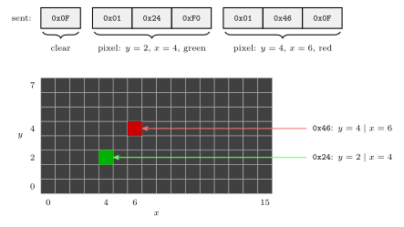
Figure 16: Seven bytes sent to the LED matrix, and what they draw. The stream divides into commands: 0x0F clears the display, and each 0x01 is followed by a position and a colour. A position byte holds y in its high nibble and x in its low nibble, so 0x24 is the pixel at x = 4, y = 2, counting from 0 at the bottom-left. A colour byte holds green in its high nibble and red in its low nibble, so 0xF0 is full green and 0x0F full red. Here red and green are the colours the LEDs show.
Worked: how fast does TCNT1 >> 8 count?
With a \(clk_{I/O}/1024\) prescaler, how quickly does TCNT1>>8 increment?
A. 7812 Hz · B. 3906 Hz · C. 1953 Hz · D. 976 Hz · E. 488 Hz · F. 244 Hz · G. 122 Hz · H. 61 Hz · I. 31 Hz · J. 15 Hz
I, 31 Hz. Timer/counter 1 counts at \(8\ \text{MHz} / 1024 = 7812.5\) counts a second. Shifting right by 8 throws away the bottom eight bits, so TCNT1>>8 goes up by one every \(2^8 = 256\) counts:
\[\frac{7812.5}{256} = 30.5\ \text{Hz}.\]
Each option is half the one before, and they line up with the shifts: A is TCNT1 itself, B is TCNT1>>1, and so on down to I for TCNT1>>8. TCNT1>>8 is the high byte of the count, 0 to 255, and it comes back round to 0 every \(65\,536 / 7812.5 = 8.4\) seconds (avr-timers-and-counters).
This is the timing the programs below use. Nothing has to be set up beyond the prescaler: the timer runs freely in normal mode, and a program that wants to do something every tenth of a second or so waits for TCNT1>>8 to move on by 3.
The tasks
- Joystick wiring test. Wire up the joystick and connect its two outputs to two LEDs on the I/O board. Wobble the stick: the LEDs’ brightness should change. Then unplug the LEDs, which upset the ADC readings if they are left connected.
- Joystick demo. Create a project with
lab16-1.c. Consult the datasheet and update the code as needed, then build and test it. - LED matrix demo. Create a project with
lab16-2.c. Consult the datasheet and update the code as needed, then build and test it. - Marquee. Needs two LED matrices, so work with someone else. Create a project with
lab16-3.c, which runs on one matrix as it is. Change it to drive two devices on the same MOSI, MISO and SCK pins but different SS pins. - Etch-A-Sketch. Create a project with
lab16-4.c: draw on the LED matrix with the joystick.
Working — Task 0
Join both + pins to VCC and one GND pin to GND. Run a wire from one L/R pin to LED L0 on the I/O board and one from a U/D pin to L1 (io-board). As the stick moves, each LED’s brightness follows the voltage on its axis, dim at one side and bright at the other. That shows both potentiometers are powered and both outputs move, before any code is involved.
Why the LEDs have to come off. A potentiometer’s wiper is a weak source. It sets the voltage, but it cannot supply current without that voltage changing. An LED draws current from it and pulls the voltage away from where the stick has put it, so the ADC would read the LED’s effect and not the stick’s position. The ADC input itself draws almost nothing.
Working — Task 1
lab16-1.c needs the converter’s register values from the datasheet. This is a complete program that does the job, to compare against. It reads both axes about ten times a second and prints them over the serial port, with the direction the stick is pushed. The serial set-up is the one from avr-usart.
#include <avr/io.h>
#include <stdint.h>

/* L/R (x) on PA0 = ADC0, U/D (y) on PA1 = ADC1.
   TXD0 (PD1) to the I/O board's serial receive, 9600 baud. */
#define X_CHANNEL 0
#define Y_CHANNEL 1

void adc_init(void) {
    ADMUX  = (1<<REFS0);                            /* AVCC, right adjusted, ADC0 */
    ADCSRA = (1<<ADEN) | (1<<ADPS2) | (1<<ADPS1);   /* on, clock = 8 MHz / 64     */
}

uint16_t adc_read(uint8_t channel) {
    ADMUX = (1<<REFS0) | channel;     /* for channel 1 this is 0x41        */
    ADCSRA |= (1<<ADSC);              /* start one conversion              */
    while (ADCSRA & (1<<ADSC)) { }    /* ADSC goes back to 0 when finished */
    return ADC;                       /* ADCL then ADCH: 0 to 1023         */
}

void uart_init(void) {
    UBRR0  = 51;                      /* 9600 baud                      */
    UCSR0B = (1<<TXEN0);              /* transmitter on; 8 data bits,   */
                                      /* no parity, 1 stop from reset   */
}

void uart_put(char c) {
    while (!(UCSR0A & (1<<UDRE0))) { }
    UDR0 = c;
}

void uart_print(const char *s) {
    while (*s) {
        uart_put(*s++);
    }
}

void uart_number(uint16_t n) {        /* four characters, right aligned */
    char d[4];
    int8_t i;

    for (i = 3; i >= 0; i--) {
        d[i] = '0' + n % 10;
        n /= 10;
    }
    for (i = 0; i < 3 && d[i] == '0'; i++) {
        d[i] = ' ';                   /* blank the leading zeros */
    }
    for (i = 0; i < 4; i++) {
        uart_put(d[i]);
    }
}

/* Which way the stick is pushed. Readings within 128 of the
   centre count as centred, so a stick at rest reads "centre". */
const char *direction(uint16_t x, uint16_t y) {
    static const char *name[3][3] = {
        /* x low        x middle    x high       */
        { "down-left", "down",     "down-right" },   /* y low    */
        { "left",      "centre",   "right"      },   /* y middle */
        { "up-left",   "up",       "up-right"   },   /* y high   */
    };
    uint8_t col = (x < 384) ? 0 : (x > 640) ? 2 : 1;
    uint8_t row = (y < 384) ? 0 : (y > 640) ? 2 : 1;
    return name[row][col];
}

int main(void) {
    uint16_t x, y;
    uint8_t now, last = 0;

    adc_init();
    uart_init();
    TCCR1A = 0;
    TCCR1B = (1<<CS12) | (1<<CS10);   /* timer 1 free running at 8 MHz / 1024 */

    while (1) {
        now = TCNT1 >> 8;                     /* advances 30.5 times a second */
        if ((uint8_t)(now - last) >= 3) {     /* so about 10 reports a second */
            last = now;
            x = adc_read(X_CHANNEL);
            y = adc_read(Y_CHANNEL);
            uart_print("x = ");
            uart_number(x);
            uart_print("   y = ");
            uart_number(y);
            uart_print("   ");
            uart_print(direction(x, y));
            uart_print("\r\n");
        }
    }
}
What each piece does.
adc_initsets the reference to AVCC and switches the converter on with its clock at 8 MHz / 64 = 125 kHz, the setting chosen above:ADPS2:0 = 110(analog-to-digital-conversion).adc_readselects the input, starts a conversion by settingADSC, and waits forADSCto drop back to 0, which the hardware does when the result is ready.REFS0is written again every time, because writingADMUXreplaces all eight bits.ADCis the 16-bit result register. The compiler reads its low byteADCLfirst and thenADCH, which is the order the hardware needs.- The pacing. Timer 1 runs freely at 8 MHz / 1024, so
TCNT1 >> 8goes up 30.5 times a second (worked above). A report goes out each time it has moved on by 3, about every 0.1 s. Subtracting asuint8_tkeeps the comparison right when the count wraps from 255 to 0. directionsorts each axis into low, middle or high with a margin of 128 either side of the centre, so that a stick at rest, which is never exactly at 511, readscentre.
Run on the joystick, it prints lines like
x =  511   y =  511   centre
x =  511   y =    0   down
x =  614   y =  689   up
x = 1023   y =  511   right
The reading (614, 689) comes out as up because its x is within the margin. At 60°, it is nearer straight up than the diagonal.
Working — Task 2
lab16-2.c needs the SPI register values from the datasheet. This program sets SPI up, sends the seven bytes decoded above, waits about two seconds, and then fills the matrix with every mix of red and green.
#include <avr/io.h>
#include <stdint.h>

#define CMD_PIXEL  0x01     /* then a position byte and a colour byte */
#define CMD_CLEAR  0x0F     /* every pixel off                         */

#define COLOUR(green, red)  (((green) << 4) | (red))    /* each 0 to 15 */

void spi_init(void) {
    DDRB  |= (1<<DDB7) | (1<<DDB5) | (1<<DDB4);   /* SCK, MOSI and SS out; MISO in */
    PORTB |= (1<<PORTB4);                          /* SS high to start with         */
    SPCR0  = (1<<SPE0) | (1<<MSTR0) | (1<<SPR10) | (1<<SPR00);   /* master, / 128  */
    /* SPI2X0 in SPSR0 stays 0 from reset */
    PORTB &= ~(1<<PORTB4);                         /* SS low: the matrix listens    */
}

uint8_t spi_send(uint8_t byte) {
    SPDR0 = byte;                       /* writing SPDR0 starts the transfer  */
    while (!(SPSR0 & (1<<SPIF0))) { }   /* SPIF0 is set after eight clocks    */
    return SPDR0;                       /* and reading SPDR0 next clears it   */
}

void matrix_clear(void) {
    spi_send(CMD_CLEAR);
}

void matrix_pixel(uint8_t x, uint8_t y, uint8_t colour) {
    spi_send(CMD_PIXEL);
    spi_send(((y & 0x07) << 4) | (x & 0x0F));   /* row high nibble, column low */
    spi_send(colour);
}

int main(void) {
    uint8_t x, y, start;

    spi_init();
    TCCR1A = 0;
    TCCR1B = (1<<CS12) | (1<<CS10);   /* 8 MHz / 1024 */

    /* the bytes 0x0F, 0x01 0x24 0xF0, 0x01 0x46 0x0F */
    matrix_clear();
    matrix_pixel(4, 2, COLOUR(15, 0));        /* green */
    matrix_pixel(6, 4, COLOUR(0, 15));        /* red   */

    start = TCNT1 >> 8;
    while ((uint8_t)((TCNT1 >> 8) - start) < 61) { }   /* about 2 seconds */

    /* every mix of the two colours: red grows to the right, green upwards */
    for (y = 0; y < 8; y++) {
        for (x = 0; x < 16; x++) {
            matrix_pixel(x, y, COLOUR(2 * y + 1, x));
        }
    }

    while (1) { }
}
Points to notice.
- Direction bits. In master mode the AVR drives SCK, MOSI and SS, so their
DDRBbits must be 1. MISO is made an input by the SPI hardware whatever itsDDRBbit says. - SS must be an output, or held high. If PB4 were an input and something pulled it low, the AVR would take that as another master claiming the bus, clear
MSTR0and drop out of master mode. As an output it is just a pin the program controls, here the matrix’s select line. spi_sendwaits onSPIF0. The flag is cleared by readingSPSR0while it is set and then readingSPDR0, which is what the loop and thereturndo. The byte returned is whatever the matrix shifted back, which these programs ignore.COLOUR(green, red)builds the colour byte from two brightnesses. The chart has red rising from 0 at the left to 15 at the right, and green from 1 at the bottom to 15 at the top. The bottom-right pixel is0x1F, nearly pure red, and the top-right is0xFF, yellow. The orange of0x7Fis at the right-hand end of row 3.- Speed. At 62.5 kHz a byte takes 128 µs, so the 128 pixel commands of the chart, 384 bytes, take about 49 ms.
Working — Task 3
Two matrices can share SCK, MOSI and MISO, because only the one whose \(\overline{\text{SS}}\) is low takes any notice of the bus. Each gets its own select line: the left matrix keeps PB4, and the right one is given PB3. The program selects a matrix, sends it complete commands, and selects the other. The two set-ups also need their grounds joined, since a signal on a wire only means something against a ground both ends share.
PB4 stays an output even when the right-hand matrix is the one selected, which keeps the AVR in master mode, for the reason given under Task 2.
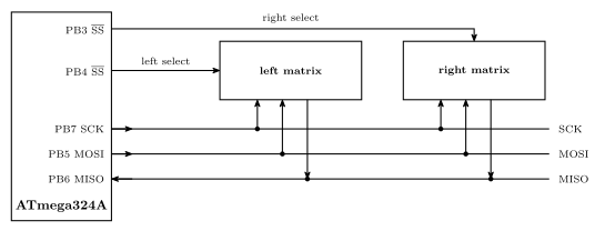
Figure 17: Two LED matrices on one SPI port. SCK, MOSI and MISO run to both, and a dot marks each real connection. Lines that cross without a dot are not connected. Each matrix has its own select line, PB4 for the left one and PB3 for the right one, and the program holds at most one of them low at a time. Only the selected matrix acts on the bytes on the bus. PB4 stays an output throughout, so the AVR stays the master.
The marquee. The message is laid out as a strip of columns: 32 blank ones, then each letter as five columns from a 5 by 7 font with one blank column after it. “CSSE2010” makes \(32 + 8 \times 6 = 80\) columns. The two matrices together are a window 32 columns wide onto the strip. At step \(s\) the left matrix shows columns \(s\) to \(s + 15\) and the right one \(s + 16\) to \(s + 31\). Each step moves the window one column to the right, which moves the text one column left, and after 80 steps the window is back at the start. The 32 blank columns let the text come in from the right-hand edge and go fully off the left before it starts again.
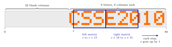
Figure 18: The marquee as a window sliding along a strip. The strip is 80 columns: 32 blank, so that the text can enter from the right, and then CSSE2010 in a 5 by 7 font with a blank column after each letter. At step s the left matrix shows columns s to s + 15 and the right matrix columns s + 16 to s + 31. Here s = 34. Each step adds 1 to s, and the text appears to move one column to the left.
#include <avr/io.h>
#include <stdint.h>

#define CMD_PIXEL  0x01
#define CMD_CLEAR  0x0F
#define COLOUR(green, red)  (((green) << 4) | (red))
#define TEXT       COLOUR(7, 15)            /* 0x7F, orange */

/* Both matrices are on SCK (PB7), MISO (PB6) and MOSI (PB5).
   Each has its own select line: the left one PB4, the right one PB3. */
#define SS_LEFT    PORTB4
#define SS_RIGHT   PORTB3

/* 5 x 7 letters, one byte per column, bit 0 the top row */
const char    letters[] = "CSE210 ";
const uint8_t font[][5] = {
    { 0x3E, 0x41, 0x41, 0x41, 0x22 },   /* C     */
    { 0x46, 0x49, 0x49, 0x49, 0x31 },   /* S     */
    { 0x7F, 0x49, 0x49, 0x49, 0x41 },   /* E     */
    { 0x42, 0x61, 0x51, 0x49, 0x46 },   /* 2     */
    { 0x00, 0x42, 0x7F, 0x40, 0x00 },   /* 1     */
    { 0x3E, 0x51, 0x49, 0x45, 0x3E },   /* 0     */
    { 0x00, 0x00, 0x00, 0x00, 0x00 },   /* space */
};

const char message[] = "CSSE2010";
#define MESSAGE_LENGTH  8
#define LEAD_IN         32                              /* blank columns first */
#define STRIP_LENGTH    (LEAD_IN + 6 * MESSAGE_LENGTH)  /* 80 columns          */

uint8_t shown[2][16];        /* the columns each matrix is showing now */

void spi_init(void) {
    DDRB  |= (1<<DDB7) | (1<<DDB5) | (1<<DDB4) | (1<<DDB3);
    PORTB |= (1<<SS_LEFT) | (1<<SS_RIGHT);       /* neither matrix selected */
    SPCR0  = (1<<SPE0) | (1<<MSTR0) | (1<<SPR10) | (1<<SPR00);
}

uint8_t spi_send(uint8_t byte) {
    SPDR0 = byte;
    while (!(SPSR0 & (1<<SPIF0))) { }
    return SPDR0;
}

void matrix_select(uint8_t m) {                  /* 0 = left, 1 = right */
    PORTB |= (1<<SS_LEFT) | (1<<SS_RIGHT);
    if (m == 0) {
        PORTB &= ~(1<<SS_LEFT);
    } else {
        PORTB &= ~(1<<SS_RIGHT);
    }
}

void matrix_pixel(uint8_t x, uint8_t y, uint8_t colour) {
    spi_send(CMD_PIXEL);
    spi_send(((y & 0x07) << 4) | (x & 0x0F));
    spi_send(colour);
}

/* Column i of the strip: 32 blank columns, then each letter
   as five columns and one blank column after it. */
uint8_t strip_column(uint8_t i) {
    uint8_t n, c, k;

    if (i < LEAD_IN) {
        return 0;
    }
    i -= LEAD_IN;
    n = i / 6;                        /* which letter of the message  */
    c = i % 6;                        /* which column of that letter  */
    if (c == 5) {
        return 0;                     /* the gap between letters      */
    }
    for (k = 0; letters[k] != message[n]; k++) { }
    return font[k][c];
}

/* Change column x of matrix m (already selected) to show bits,
   sending only the pixels that differ from what it shows now. */
void show_column(uint8_t m, uint8_t x, uint8_t bits) {
    uint8_t changed = bits ^ shown[m][x];
    uint8_t k;

    for (k = 0; k < 7; k++) {
        if (changed & (1<<k)) {
            matrix_pixel(x, 7 - k, (bits & (1<<k)) ? TEXT : 0x00);
        }
    }
    shown[m][x] = bits;
}

int main(void) {
    uint8_t step = 0, m, x, now, last;

    spi_init();
    TCCR1A = 0;
    TCCR1B = (1<<CS12) | (1<<CS10);         /* TCNT1 >> 8 counts at 30.5 Hz */

    for (m = 0; m < 2; m++) {
        matrix_select(m);
        spi_send(CMD_CLEAR);
    }

    last = TCNT1 >> 8;
    while (1) {
        now = TCNT1 >> 8;
        if ((uint8_t)(now - last) >= 3) {   /* one step about every 0.1 s */
            last = now;
            for (m = 0; m < 2; m++) {
                matrix_select(m);
                for (x = 0; x < 16; x++) {
                    show_column(m, x, strip_column((step + 16 * m + x) % STRIP_LENGTH));
                }
            }
            step = (step + 1) % STRIP_LENGTH;
        }
    }
}
How it works.
- The font. Each letter is five bytes, one per column, with bit 0 the top row. A row number \(k\) from the top becomes \(y = 7 - k\) on the matrix, so the letters fill rows 7 down to 1 and row 0 stays blank.
- Only changes are sent.
shownremembers what each column of each matrix is showing. XOR with the new column gives a 1 for every pixel that has to change, and only those get a command. Redrawing both matrices in full would be \(2 \times 128 \times 3 = 768\) bytes, about 0.1 s at 128 µs a byte, which would use up the whole step. Sending only the changes is a few dozen pixels a step. - Selecting.
matrix_selectraises both select lines and then lowers one, so the two are never low together, and it is only called between complete commands. A matrix deselected halfway through a command would be left waiting for the rest of it. - The pace is three counts of
TCNT1 >> 8, \(3 \times 256 / 7812.5 = 98\) ms a step, so the 80-step cycle takes just under 8 seconds.
Working — Task 4
The Etch-A-Sketch has a pen, a red pixel that blinks, and the stick moves it one pixel at a time. Wherever the pen has been is left green. A push of button B0 on the I/O board, wired to PD2, wipes the drawing.
#include <avr/io.h>
#include <stdint.h>

#define CMD_PIXEL  0x01
#define CMD_CLEAR  0x0F
#define COLOUR(green, red)  (((green) << 4) | (red))
#define TRAIL      COLOUR(15, 0)     /* green: the line drawn */
#define PEN        COLOUR(0, 15)     /* red: where the pen is */
#define BLANK      0x00

/* Joystick x on PA0 (ADC0), y on PA1 (ADC1). LED matrix on PB7 to PB4.
   Push button B0 on PD2 clears the drawing. */

uint8_t drawn[16];           /* bit y of drawn[x] is 1 where the line has been */

void adc_init(void) {
    ADMUX  = (1<<REFS0);
    ADCSRA = (1<<ADEN) | (1<<ADPS2) | (1<<ADPS1);
}

uint16_t adc_read(uint8_t channel) {
    ADMUX = (1<<REFS0) | channel;
    ADCSRA |= (1<<ADSC);
    while (ADCSRA & (1<<ADSC)) { }
    return ADC;
}

void spi_init(void) {
    DDRB  |= (1<<DDB7) | (1<<DDB5) | (1<<DDB4);
    PORTB |= (1<<PORTB4);
    SPCR0  = (1<<SPE0) | (1<<MSTR0) | (1<<SPR10) | (1<<SPR00);
    PORTB &= ~(1<<PORTB4);
}

uint8_t spi_send(uint8_t byte) {
    SPDR0 = byte;
    while (!(SPSR0 & (1<<SPIF0))) { }
    return SPDR0;
}

void matrix_pixel(uint8_t x, uint8_t y, uint8_t colour) {
    spi_send(CMD_PIXEL);
    spi_send(((y & 0x07) << 4) | (x & 0x0F));
    spi_send(colour);
}

void clear_drawing(void) {
    uint8_t x;

    spi_send(CMD_CLEAR);
    for (x = 0; x < 16; x++) {
        drawn[x] = 0;
    }
}

/* -1, 0 or +1 for one axis: it has to be pushed past half way */
int8_t step_for(uint16_t reading) {
    if (reading < 256) {
        return -1;
    }
    if (reading > 767) {
        return 1;
    }
    return 0;
}

int main(void) {
    uint8_t x = 8, y = 4;                /* the pen starts in the middle */
    int8_t nx, ny;
    uint8_t now, last_move, blink, shown_blink = 2;
    uint8_t button, last_button = 0;

    adc_init();
    spi_init();
    DDRD &= ~(1<<DDD2);                  /* the clear button is an input */
    TCCR1A = 0;
    TCCR1B = (1<<CS12) | (1<<CS10);      /* 8 MHz / 1024 */

    clear_drawing();
    last_move = TCNT1 >> 8;

    while (1) {
        /* clear on the push of the button, not for as long as it is held */
        button = (PIND >> PIND2) & 1;
        if (button && !last_button) {
            clear_drawing();
            shown_blink = 2;             /* make the pen be drawn again */
        }
        last_button = button;

        /* move at most one pixel every 4 counts of TCNT1 >> 8: 7.6 a second */
        now = TCNT1 >> 8;
        if ((uint8_t)(now - last_move) >= 4) {
            last_move = now;
            nx = x + step_for(adc_read(0));
            ny = y + step_for(adc_read(1));
            if (nx < 0)  { nx = 0; }
            if (nx > 15) { nx = 15; }
            if (ny < 0)  { ny = 0; }
            if (ny > 7)  { ny = 7; }
            if (nx != x || ny != y) {
                drawn[x] |= (1<<y);          /* leave the line where the pen was */
                matrix_pixel(x, y, TRAIL);
                x = nx;
                y = ny;
                shown_blink = 2;
            }
        }

        /* the pen blinks: bit 12 of TCNT1 flips every 4096 counts, 0.52 s */
        blink = (TCNT1 >> 12) & 1;
        if (blink != shown_blink) {
            if (blink) {
                matrix_pixel(x, y, PEN);
            } else {
                matrix_pixel(x, y, (drawn[x] & (1<<y)) ? TRAIL : BLANK);
            }
            shown_blink = blink;
        }
    }
}
How it works.
- Reading the stick as a step.
step_forturns a reading into \(-1\), 0 or \(+1\), with the stick pushed past half way, below 256 or above 767, before it counts. Both axes are read each time, so a diagonal push moves the pen diagonally. - Pacing from the timer. The pen moves at most once per 4 counts of
TCNT1 >> 8, which is \(4 \times 256 / 7812.5 = 131\) ms, about 7.6 moves a second. Without it the pen would cross the matrix in a few milliseconds. - Blinking from the timer. Bit 12 of
TCNT1changes every \(2^{12} = 4096\) counts, 0.52 s, so(TCNT1 >> 12) & 1is a square wave with a period of just over a second, for nothing more than a read of the count. The pixel is only resent when that bit changes, not on every pass of the loop. - Remembering the drawing.
drawnholds one bit per pixel, so that when the pen blinks off it shows the line underneath, or nothing, as it should. shown_blink = 2is a value the bit can never have, which forces the pen to be redrawn on the next pass after a move or a clear.- The button clears on its rising edge, the moment it goes down, using the same comparison with the previous reading as the stopwatch in week9-lab-avr-interrupts.
Which way is up. The program moves the pen in the joystick’s own frame: right with x, up with y. Set in the breadboard as described above, the joystick’s x points to the top of the breadboard (Figure 11), so pushing the stick away moves the pen right. To have the pen follow the stick as seen from in front of the breadboard, swap the axes and reverse one: move right as y falls and up as x rises, which is nx = x - step_for(adc_read(1)) and ny = y + step_for(adc_read(0)).
See also
- analog-to-digital-conversion — the converter’s registers, its clock, a conversion step by step
- avr-spi — the SPI bus, its registers and the shift-register ring
- io-board — the joystick’s pins and the LED matrix’s commands
- avr-timers-and-counters — the prescaler and the slow count from
TCNT1 >> 8 - avr-usart — the serial port Task 1 prints through
- polling-and-interrupts — the two ways to wait for a conversion or a transfer
- week9-lab-avr-interrupts — Lab 14
- 2026-09-24-serial-io — Lecture 18 · 2026-10-05-more-io — Lecture 19
Reference material
Analog to Digital Conversion
Turning a voltage into a number the processor can use. A digital input pin only distinguishes 0 from 1. An analog to digital converter (ADC) reports how big a voltage is, to a fixed number of bits. First met in 2026-09-24-serial-io, and used to read a joystick in week10-lab-adc-and-spi.
What a converter does
An ADC takes an input voltage between 0 and a maximum, the reference voltage \(V_{ref}\), and produces an unsigned integer in proportion to it. Zero volts gives 0, and a voltage just under \(V_{ref}\) gives the largest value the result can hold.
The number of bits in the result is the converter’s resolution. With \(n\) bits there are \(2^n\) possible results, 0 to \(2^n - 1\):
| Resolution | Results | Range |
|---|---|---|
| 8 bits | 256 | 0 to 255 |
| 10 bits | 1024 | 0 to 1023 |
| 12 bits | 4096 | 0 to 4095 |
From voltage to number
The converter divides the range from 0 to \(V_{ref}\) into \(2^n\) equal steps and reports which step the input is on. For a 10-bit converter:
\[\text{result} = \left\lfloor \frac{V_{in}}{V_{ref}} \times 1024 \right\rfloor, \qquad \text{at most } 1023\]
and the size of one step is
\[\frac{V_{ref}}{1024} = \frac{5\ \text{V}}{1024} \approx 4.9\ \text{mV} \quad\text{when } V_{ref} = 5\ \text{V}.\]
| \(V_{in}\) (with \(V_{ref}\) = 5 V) | Result |
|---|---|
| 0 V | 0 |
| 1.25 V | 256 |
| 2.5 V | 512 |
| 3.75 V | 768 |
| 5 V | 1023 |
Two things follow from the staircase in Figure 19.
- The result is rounded down to a step. Every voltage within one step gives the same number, so a result is only known to within one step, 4.9 mV here. More bits means smaller steps.
- The top result is \(2^n - 1\), not \(2^n\). There are 1024 steps numbered from 0, so full scale reads 1023.
Going the other way, a result \(r\) stands for a voltage of about \(r \times V_{ref} / 1024\). A reading of 300 with a 5 V reference is about \(300 \times 4.88\ \text{mV} = 1.46\ \text{V}\).
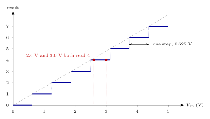
Figure 19: Conversion with a 3-bit converter and a 5 V reference, drawn with few enough steps to see. The input range is cut into \(2^3 = 8\) equal steps of 0.625 V, and the result is the number of the step the input is on, from 0 to 7. Every voltage within a step gives the same result, so 2.6 V and 3.0 V both read 4. A 10-bit converter does the same thing with 1024 steps of about 4.9 mV.
The ATmega324A’s converter
- Inputs. The eight port A pins can be used as analog inputs. A pin used this way is not read through
PINA. The result comes from the converter’s own data register,ADC, which is 16 bits wide to hold the 10-bit result. - One at a time. There is a single converter, with an analog multiplexer in front of it that connects one of the pins to it. To read two voltages, such as the two axes of a joystick, select one pin and convert, then select the other and convert.
- Reference. \(V_{ref}\) can be chosen. The course uses the supply, \(V_{cc} = 5\ \text{V}\).
- Resolution. 10 bits: results from 0 to 1023.
- Time. A conversion is not instant. It takes up to 3200 clock cycles, which is 0.4 ms with the 8 MHz clock. The converter can be run faster at the cost of accuracy.
Because a conversion takes thousands of clock cycles, starting one and getting the answer are separate moments. Between them the program either waits and checks whether the converter has finished, or does something else and lets the converter raise an interrupt when it has (polling-and-interrupts). The interrupt has its own vector, written ISR(ADC_vect) in C (avr-interrupts).
Worked: a joystick
A joystick gives two voltages between 0 and 5 V, one for left-right and one for up-down. Pushed three-quarters of the way right and a quarter of the way up, it gives 3.75 V and 1.25 V, which convert to 768 and 256. Centred, each axis is near 2.5 V and reads near 512. Each reading takes its own conversion, so the two numbers are from slightly different moments.
Inside, each axis is a potentiometer between 5 V and ground, and the stick moves its wiper, so the wiper’s voltage follows the stick from one side to the other (io-board).
Worked: where is the stick?
A joystick’s reading is easiest to interpret measured from the centre. Half of 1023 is 511.5, so 511 and 512 do equally well as the centre. Taking 511 on both axes,
\[\Delta x = x - 511, \qquad \Delta y = y - 511,\]
the direction of the stick is the angle \(\tan^{-1}(\Delta y / \Delta x)\), measured anticlockwise from straight right and put in the right quadrant by the signs, and how far it is pushed is \(\sqrt{\Delta x^2 + \Delta y^2} / 511\) of full deflection.
- (511, 0): \(\Delta x = 0\), \(\Delta y = -511\). Straight down, all the way.
- (614, 689): \(\Delta x = 103\), \(\Delta y = 178\). The angle is \(\tan^{-1}(178/103) = 60^\circ\), and the distance is \(\sqrt{103^2 + 178^2} = 206\), which is \(206 / 511 = 40\,\%\) of full deflection.
The readings themselves are never negative: \(\Delta x\) and \(\Delta y\) are what a program works out, not what the converter reports. And the centre is only roughly 511, since a real stick at rest sits a few counts to one side, so a program tests against a margin, as in week10-lab-adc-and-spi.
The registers
A program runs the converter through three registers, counting the 16-bit result as one:
| Register | Holds |
|---|---|
ADMUX |
which reference, which input, and how the result is lined up |
ADCSRA |
on and off, start, the finished flag and its interrupt enable, and the clock prescaler |
ADC, as ADCH and ADCL |
the result |
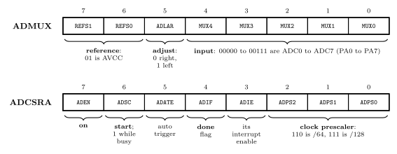
Figure 20: The converter’s two control registers, with their bits grouped by what they do. In ADMUX the top two bits choose the reference voltage, bit 5 chooses whether the 10-bit result is lined up at the right or the left of its 16-bit register, and the bottom five choose the input pin. In ADCSRA bit 7 switches the converter on, bit 6 starts a conversion and stays 1 while it runs, bit 4 is the flag set when a result is ready and bit 3 its interrupt enable, and the bottom three bits divide the system clock down to the converter’s own clock.
ADMUX: what to convert
REFS1 |
REFS0 |
Reference voltage |
|---|---|---|
| 0 | 0 | whatever is on the AREF pin |
| 0 | 1 | AVCC, the converter’s supply, 5 V on the lab boards |
| 1 | 0 | an internal 1.1 V |
| 1 | 1 | an internal 2.56 V |
ADLAR, ADC left adjust result, is 0 for a result lined up at the right of the 16-bit register, so that it reads as a number from 0 to 1023. Set to 1, it is lined up at the left instead (below).MUX4:0picks the input.00000to00111are the pins ADC0 to ADC7, which are PA0 to PA7, each on its own. The other codes select differential pairs of pins and two internal test voltages, which the course does not use.
Worked: the value for ADC1
AVCC as the reference, right adjusted, input ADC1:
\[\underbrace{01}_{\texttt{REFS1:0}}\ \underbrace{0}_{\texttt{ADLAR}}\ \underbrace{00001}_{\texttt{MUX4:0}} = \texttt{0100 0001} = \texttt{0x41}\]
In C, ADMUX = (1<<REFS0) | 1;. Writing the register replaces all eight bits, so the reference bits have to be included every time the input is changed. ADMUX = 1; alone would select ADC1 with the AREF pin as the reference, which on a board with nothing connected to AREF gives meaningless results.
ADCSRA: control and status
| Bit | Name | |
|---|---|---|
| 7 | ADEN |
enable: 1 switches the converter on. Nothing happens without it |
| 6 | ADSC |
start conversion: write a 1 to start one. It reads 1 while the conversion runs and drops to 0 when the result is ready |
| 5 | ADATE |
auto trigger: start conversions automatically, for example one after another. Left 0 here |
| 4 | ADIF |
interrupt flag: set when a conversion finishes. Cleared by writing a 1 to it, or by the hardware when the interrupt is taken |
| 3 | ADIE |
interrupt enable for that flag |
| 2–0 | ADPS2:0 |
prescaler: what the system clock is divided by to make the ADC clock |
ADPS2:0 |
000 | 001 | 010 | 011 | 100 | 101 | 110 | 111 |
|---|---|---|---|---|---|---|---|---|
| Divide by | 2 | 2 | 4 | 8 | 16 | 32 | 64 | 128 |
| ADC clock at 8 MHz | 4 MHz | 4 MHz | 2 MHz | 1 MHz | 500 kHz | 250 kHz | 125 kHz | 62.5 kHz |
ADEN and the prescaler are set once. ADSC is set for every conversion.
The result: ADCH and ADCL
The 10-bit result sits in a 16-bit register made of two bytes, ADCH and ADCL. ADLAR decides where.
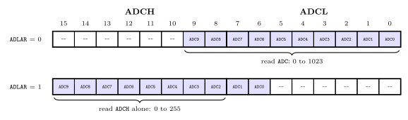
Figure 21: Where the 10 result bits go in ADCH:ADCL. Right adjusted, with ADLAR = 0, bits 9 and 8 are the bottom two bits of ADCH and the rest fill ADCL, so the 16-bit register reads as a number from 0 to 1023 and the six unused bits are 0. Left adjusted, with ADLAR = 1, the result starts at the top, so ADCH on its own holds the top 8 bits, a result from 0 to 255 for a program that does not need all 10.
- Read the low byte first. Reading
ADCLlocks the register, so that a conversion finishing in between cannot replace one byte and not the other, and readingADCHunlocks it. The order isADCL, thenADCH. - In C, read
ADC. The header definesADCas the 16-bit register, and the compiler reads the two bytes in the right order. - Left adjusted,
ADCHalone will do. WithADLAR= 1 the top 8 bits are all inADCH, and readingADCHby itself is allowed. It gives an 8-bit result, steps of about 20 mV with a 5 V reference.
The ADC clock
The converter has its own clock, made by dividing the system clock with the prescaler in ADCSRA. For the full 10 bits of precision, the ADC clock must be between 50 kHz and 200 kHz. A faster clock gives a quicker conversion with fewer accurate bits, which is the trade between accuracy and speed.
A conversion takes 13 ADC clock cycles. The first one after ADEN is set takes 25, because the analog circuits have to settle. At the slowest setting, the system clock divided by 128, that first conversion is \(25 \times 128 = 3200\) system clock cycles, 0.4 ms at 8 MHz, which is the “up to 3200 clock cycles” above.
Worked: choosing the prescaler
With the 8 MHz system clock, the ADC clock is \(8\ \text{MHz} / N\). For it to lie between 50 and 200 kHz,
\[\frac{8\ \text{MHz}}{200\ \text{kHz}} \le N \le \frac{8\ \text{MHz}}{50\ \text{kHz}} \quad\Longrightarrow\quad 40 \le N \le 160.\]
Of the settings on offer, 64 (125 kHz) and 128 (62.5 kHz) are in range. Either is right. 64 is the faster of the two: a conversion takes \(13 \times 64 = 832\) system cycles, 104 µs.
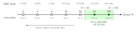
Figure 22: The prescaler settings against the window for full precision. Each setting divides the 8 MHz system clock, giving the ADC clock above the axis and the time for one 13-cycle conversion below it. Only the shaded band, an ADC clock from 50 to 200 kHz, gives all 10 bits. That band is a divisor from 40 to 160, and the two settings inside it are 64 and 128. Settings to the left are faster but less accurate.
A conversion, step by step
- Choose the reference and the input in
ADMUX. - Switch on the converter and set its clock:
ADENand the prescaler bits inADCSRA. Once is enough. - Start a conversion by setting
ADSC. - Wait until it has finished.
ADSCreads 1 until then, and at the end the hardware clears it and setsADIF. - Read the result from
ADC.
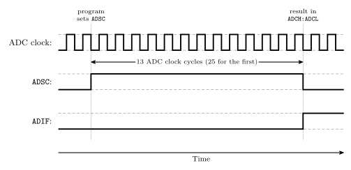
Figure 23: One conversion against time. The program writes a 1 to ADSC and the conversion starts. ADSC stays at 1 for the 13 cycles of the ADC clock that the conversion takes, 25 for the first one after the converter is switched on. At the end the hardware puts ADSC back to 0, sets the flag ADIF and leaves the new result in ADCH:ADCL. A program can wait for either bit, or enable the interrupt and be told.
By polling. Wait for ADSC to drop:
#include <avr/io.h>
#include <stdint.h>

uint16_t adc_read(uint8_t channel) {
    ADMUX = (1<<REFS0) | channel;     /* AVCC, right adjusted, this input */
    ADCSRA |= (1<<ADSC);              /* start                             */
    while (ADCSRA & (1<<ADSC)) { }    /* busy while ADSC reads 1           */
    return ADC;                       /* ADCL, then ADCH                   */
}

int main(void) {
    uint16_t x, y;

    ADCSRA = (1<<ADEN) | (1<<ADPS2) | (1<<ADPS1);   /* on, 8 MHz / 64 = 125 kHz */
    while (1) {
        x = adc_read(0);
        y = adc_read(1);
        (void)x; (void)y;
    }
}
Waiting on ADSC needs no clearing up afterwards. Waiting on ADIF works too, but the flag stays set until a 1 is written to it, so the program has to clear it before the next conversion.
By interrupt. Set ADIE and write a handler for ADC_vect (avr-interrupts). The handler here collects each result and starts the next conversion, so the converter runs continuously and the main program reads the latest value whenever it wants one:
#include <avr/io.h>
#include <avr/interrupt.h>
#include <stdint.h>

volatile uint16_t latest;             /* the newest result */

ISR(ADC_vect) {
    latest = ADC;                     /* ADIF is cleared as the handler starts */
    ADCSRA |= (1<<ADSC);              /* start the next conversion             */
}

int main(void) {
    uint16_t x;

    ADMUX  = (1<<REFS0);                                      /* AVCC, ADC0 */
    ADCSRA = (1<<ADEN) | (1<<ADIE) | (1<<ADPS2) | (1<<ADPS1); /* / 64       */
    sei();
    ADCSRA |= (1<<ADSC);              /* the first conversion */

    while (1) {
        cli();                        /* a 16-bit copy must not be split */
        x = latest;
        sei();
        /* ... use x ... */
        (void)x;
    }
}
latest is two bytes, so the main program copies it with interrupts off, for the reason in software-timers.
Changing input. A change to ADMUX during a conversion only takes effect when that conversion has finished. Change the input between conversions, as adc_read does.
Common mistakes
- Expecting 1024 at full scale. The largest 10-bit result is 1023.
- Forgetting the reference. The same result means a different voltage with a different \(V_{ref}\). A result is a fraction of the reference.
- Treating the result as exact. It is the step the voltage was on, good to one step.
- Expecting two inputs to be read together. One converter, one input at a time.
- Using the result the instant a conversion is started. It is not ready for up to 0.4 ms.
- Forgetting
ADEN. SettingADSCon a converter that is switched off starts nothing. - Losing the reference bits.
ADMUX = 1;selects ADC1 but also setsREFS1:0to00, the AREF pin. Keep(1<<REFS0)in every write. - A prescaler outside the window. At 8 MHz only 64 and 128 put the ADC clock between 50 and 200 kHz. Anything faster gives fewer good bits.
- Reading
ADCHbeforeADCL. ReadingADCLlocks the result untilADCHis read. Read the 16-bitADCin C and the order is right. - Expecting negative readings. The result is unsigned, 0 to 1023. A joystick’s offset from its centre is something the program works out by subtracting.
- Loading the input. An LED, or the pin’s own pull-up resistor switched on through
PORTA, draws current from the voltage being measured and changes it. A potentiometer’s wiper in particular cannot supply current without its voltage moving.
See also
- 2026-09-24-serial-io — Lecture 18, where the converter is introduced
- week10-lab-adc-and-spi — Lab 16: the prescaler and
ADMUXworked, reading a joystick, and four programs that use it - io-board — the joystick module and its pins
- avr-io-ports — the digital side of the same pins
- polling-and-interrupts · avr-interrupts — the two ways to find out a conversion has finished
- avr-architecture — the A/D converter on the block diagram
- binary-number-representations — unsigned integers, and why 10 bits hold 0 to 1023
The Assembly Process
How an assembly language program becomes machine code. It covers the four fields of a statement, the directives that tell the assembler what to do as opposed to the CPU, the three memory segments of the AVR and the location counter that walks through each, and the two-pass assembler with its symbol table, which is how a program can jump to a label it has not reached yet. The program skeleton these pieces fit into is avr-program-structure, and the memories the segments map onto are in memory-models and avr-architecture. First met in 2026-10-08-assembly-process.
What an assembler does
An assembler turns a text file of assembly language into the bits that go into the chip’s memories. Most of that is translation, one statement at a time: add r1, r2 has a fixed binary form, 0000 1100 0001 0010, and nothing else in the file can change it (avr-instructions). Each instruction becomes exactly one machine instruction (instruction-set-architecture).
Two things make it more than a lookup table:
- A program is more than instructions. It has to say where things go in memory, reserve space for variables, put constant tables in flash and give registers and addresses readable names. None of that is an instruction for the CPU. These lines are directives, commands to the assembler itself.
- Names stand for numbers that are not known yet.
jmp RESETneeds the address ofRESET, and ifRESET:is further down the file, a single read from top to bottom cannot supply it. The cure is to read the file twice.
C reaches machine code by a different road: the compiler turns one line of C into many instructions (2026-09-07-introduction-to-embedded-c-programming), and how that output is joined into a program is compilation-and-linking.
The format of a statement
An assembly program is a sequence of one-line statements. A statement has up to four fields, and any of them may be empty:
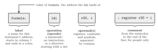
Figure 24: The four fields of one assembly statement. The label names the address this statement ends up at, so other statements can jump to it or refer to the data there. The operation field holds the mnemonic, which is either an instruction for the CPU or, if it starts with a dot, a directive for the assembler. The operands are what the operation works on: registers, constants or symbols, separated by commas. The comment runs from the semicolon to the end of the line and is thrown away by the assembler.
Label. A name for a position in memory. Labels exist so that statements can be jumped to and so that data can be referred to by name. Its value is the address the statement lands at: a word address in program memory for code, a byte address in data memory for a variable. By convention a label starts in column 1 and everything else is indented, so labels stand out down the left edge. In AVR assembly it ends with a colon.
Operation. A symbolic abbreviation for an instruction’s opcode, a mnemonic: LDS for Load Direct from data Space, ldi for load immediate. Or a directive, which starts with a dot.
Operands. The registers and addresses the instruction uses. Register names belong to the machine:
| Machine | Register names |
|---|---|
| Pentium | eax, ebx, esi, edi, … |
| SPARC | o0..o7, i0..i7, l0..l7, g0..g7 (out, in, local and global) |
| AVR | simply r0..r31 |
An address operand is usually written as a label, lds r16, count, and the assembler substitutes the number.
Comment. Space for explanation, only for people: the assembler discards it. In assembly comments are not optional politeness. ldi r20, 13 says nothing about why; the comment is the only place the intent is written down.
Ending a statement. Some assemblers want a semicolon at the end of every statement and others do not. AVR assembly does not: the end of the line ends the statement, and a semicolon starts a comment.
Directives
Besides instructions, the assembler needs other information, for example:
- where in memory the code and data should go;
- nicer names for registers and addresses, such as
tempforr16orSPHfor I/O address0x3E; - space for variables and tables of constants.
That information is given as a directive, also called a pseudo-instruction: a command to the assembler itself, written where an instruction would be and preceded by a dot, as in .byte or .def temp = r16. Most directives produce no machine code at all. They change what the assembler knows or where it is putting things.
The assembler in Microchip Studio, AVRASM2, has these, among others:
| Directive | What it does |
|---|---|
.byte |
reserve bytes for a variable |
.cseg |
switch to the code segment |
.csegsize |
set the program memory size |
.db |
define constant byte(s) |
.def |
give a register a symbolic name |
.device |
name the exact processor the program is for |
.dseg |
switch to the data segment |
.dw |
define constant word(s) |
.equ |
set a symbol equal to an expression, permanently |
.eseg |
switch to the EEPROM segment |
.exit |
stop processing this file |
.include |
read source from another file, here |
.list, .nolist |
turn generation of the list file on, off |
.listmac |
show macro expansions in the list file |
.macro, .endm (or .endmacro) |
begin, end a macro |
.org |
set the location counter: the address of what comes next |
.set |
set a symbol equal to an expression, changeably |
.if, .else, .elif, .endif |
conditional assembly: include lines only if a condition holds |
All of this is AVRASM2’s syntax. Other assemblers, even ones for the AVR, spell things differently. The GNU assembler used behind avr-gcc has a .byte directive too, and there it stores the bytes listed instead of reserving space.
Segments and location counters
The AVR has three memories (avr-architecture), and to the assembler each is a segment. Directives choose which segment the following lines go into:
| Segment | Directive | Memory | What can go there |
|---|---|---|---|
| code | .cseg |
flash, program memory | instructions, and constant data |
| data | .dseg |
SRAM, data memory | space only, reserved for variables |
| EEPROM | .eseg |
EEPROM | constants |
The data segment cannot be given values. The assembler’s output is programmed into flash and EEPROM, which keep their contents with the power off. SRAM is empty at power-up and holds nothing until the running program writes to it, so all the assembler can do there is decide which addresses each variable will use.
Each segment has its own location counter: the address the next thing in that segment will be placed at. A label takes the current value of its segment’s counter, and every statement that places something advances the counter by its size. Switching segment does not reset anything. It only changes which counter is in use, so a segment can be built up in pieces, and each piece carries on where the last piece of the same segment stopped.
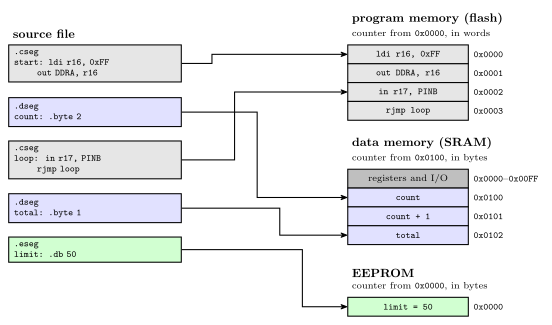
Figure 25: One source file feeding three memories. The file switches segment four times, and each piece goes to the memory its directive names, carrying on from where the previous piece of the same segment stopped: the second code piece follows the first in flash, and total follows count in SRAM. Each segment has its own location counter. The code counter starts at 0 and counts 16-bit words. The data counter starts at 0x0100, the first address after the registers and I/O, and counts bytes. The EEPROM counter starts at 0 and counts bytes. Grey marks code, blue data and green EEPROM.
Where each counter starts:
- Code: at 0, the reset address, and the assembler starts in the code segment, so a file with no segment directives is all code. The counter counts 16-bit words, because each program-memory address names a word (memory-models).
- Data: at the first free SRAM address,
0x0100on the ATmega324A, since0x0000to0x00FFare the registers and I/O registers. The counter counts bytes. - EEPROM: at 0, counting bytes.
.org sets the counter of the current segment to a given value, so whatever follows is placed there. It works in any segment, in that segment’s units.
Reserving and defining data
Three directives put data in memory:
| Directive | Segment | Places | Size |
|---|---|---|---|
.byte n |
data | nothing: reserves n bytes |
n bytes |
.db a, b, … |
code or EEPROM | constant bytes, 8 bits each | one byte each |
.dw a, b, … |
code or EEPROM | constant words, 16 bits each | two bytes each |
.byte is allowed only in the data segment: it is how a variable gets an address. .db and .dw initialise constants, so they belong where constants can live: the code segment or the EEPROM segment.
.db in the code segment packs two bytes per word. Program memory is 16 bits wide, so consecutive bytes share a word, the first in the low byte and the second in the high byte. A .db line with an odd number of bytes leaves half a word over, and the assembler fills it with a zero pad byte so that the next line starts on a whole word. Each .db line is padded on its own, so two 5-byte lines take 3 words each, not 5 words between them. AVRASM2 warns when it pads. Writing the 0 yourself gives the same layout without the warning.
.dw takes one whole word per value, so it is the natural way to store numbers bigger than 255, or addresses.
Worked: a lookup table in flash
A lookup table (LUT) is a table of constants a program reads instead of computing. Lay out:
        .cseg
table1: .db  11, 12, 30
table2: .dw  100, 133
        .org 500
table3: .dw  ...
The code counter starts at 0.
table1= 0. Three bytes: 11 and 12 share word 0, 30 takes the low half of word 1, and a pad 0 fills its high half. The counter moves to 2.table2= 2. Two words, 100 at word 2 and 133 at word 3. The counter moves to 4..org 500sets the counter to 500. Words 4 to 499 are skipped, and nothing is placed there.table3= 500 (0x01F4).
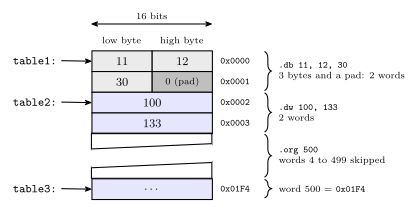
Figure 26: The lookup table laid out in program memory, one 16-bit word per row, lowest address at the top. A .db puts two bytes in each word, the first in the low byte, and pads an odd count with a zero byte so that the next label starts on a whole word: here 30 shares word 1 with a pad. Each .dw value fills a whole word. The .org moves the location counter forward and leaves words 4 to 499 untouched, so table3 lands at word 500. The diagonal break means the gap is not drawn to scale. Grey marks the .db bytes, dark grey the pad and blue the .dw words.
On the data side, two .byte 2 lines in separate .dseg pieces end up next to each other, at 0x0100 and 0x0102, whatever code sits between them in the file. That is worked in 2026-10-08-assembly-process.
Naming things: .def, .equ and .set
Three directives give a name to something. None of them places anything or moves a location counter.
| Directive | Names | Can it be changed later? | Example |
|---|---|---|---|
.def |
a register, and only a register | yes, by another .def |
.def ZH = r31 |
.equ |
a value: a number, an I/O address, an expression | no | .equ sreg = 0x3f ; Status register |
.set |
a value | yes, by another .set |
.set io_offset = 0x23 ; For now |
.equ is the usual choice for a constant, because a second definition is an error and catches a clash of names. .set is for a value that a later part of the file deliberately redefines, which is what for now in the comment above says.
Check. The same program defines .equ SPH = $3E and .def ZH = r31. Why .equ for one and .def for the other? SPH is an I/O register, which instructions such as out reach by its I/O address, 0x3E. To the assembler that is just a number, so .equ. ZH is general-purpose register r31, the high byte of the Z pointer, which instructions name as a register operand, so .def.
Two more directives are about files and the processor rather than names:
.include "file"reads another file in at that point, as if its text were typed there..include "m324Adef.inc"is howPORTA,SPH,RAMENDand the rest get defined: the file is mostly.equand.deflines (avr-io-ports)..device ATmega324Anames the exact processor. The assembler then rejects any instruction that chip does not implement..exitstops reading the file at that line. Anything after it is ignored.
The forward reference problem
Read top to bottom, most statements can be translated on the spot. add r1, r2 names two registers and nothing else, so its machine word is known at once.
A label used before it is defined is different. A program usually starts with
        jmp  RESET
        ...
RESET:  ldi  temp, low(RAMEND)
When the assembler reaches the jmp, it knows the opcode but not the operand: RESET has not been seen, so there is no address to put in the instruction. This is the forward reference problem. One forward reference anywhere in a file is enough to stop a single top-to-bottom pass from finishing the job.
The two-pass assembler
The fix is to process the file twice.
Pass one: define every symbol. Go through the file without generating anything. Keep a location counter for each segment, starting at 0 for code and EEPROM and at 0x0100 for data. For each line:
- if it has a label, enter the label in the symbol table with its segment and the current value of that segment’s counter;
- if it is
.equ,.setor.def, enter that name and its value; - if it is
.cseg,.dsegor.eseg, switch counters; if it is.org, set the current counter; - advance the current counter by the line’s size: 1 or 2 words for an instruction, the padded number of words for
.db, a word per value for.dw,nbytes for.byte n, and 0 for a line that only names something.
Pass one only needs each line’s size, and every instruction’s size is known without knowing its operands: jmp RESET takes 2 words whatever RESET turns out to be.
Pass two: assemble. Go through the file again with the counters reset. Now every symbol’s value is in the table, so each instruction can be assembled, turned into actual machine code, with its operands filled in, and each .db and .dw value can be written.
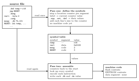
Figure 27: The two-pass assembler. Pass one reads the whole source and produces no code: it steps the location counters and records each symbol’s segment and value in the symbol table. Pass two reads the same source again from the top and, with every value now in the table, encodes each instruction and writes each constant. Its output is the contents of flash and of EEPROM. The data segment produces no output, only the addresses its labels were given.
Worked: a two-pass trace
The program:
        .equ    RAMEND = $08FF
        .equ    SPH = $3E
        .equ    SPL = $3D
        .def    ZH = r31
        .def    ZL = r30
        jmp     RESET
        .dseg
var1:   .byte   2
var2:   .byte   2
        .cseg
        .def    temp = r16
mesg:   .db     72,101,108,108,111
table:  .dw     var1, var2
RESET:  ldi     temp, low(RAMEND)
        out     SPL, temp
        ldi     temp, high(RAMEND)
        out     SPH, temp
        ...
        ldi     ZH, high(mesg*2)
        ldi     ZL, low(mesg*2)
        lpm                     ;R0 <= M[Z]
Pass one. The code counter starts at 0 and the data counter at 0x0100 (256).
- The five
.equand.deflines enterRAMEND,SPH,SPL,ZHandZLin the table and place nothing. jmp RESETis a 2-word instruction, so it takes words 0 and 1 and the code counter goes to 2.RESETis not known yet, and pass one does not need it to be..dsegswitches to the data counter.var1= 256 (0x0100) and.byte 2moves the counter to 258.var2= 258 (0x0102) and the counter goes to 260..csegswitches back to the code counter, still at 2..def temp = r16enterstemp.mesg= 2. Five bytes need three words with a pad, words 2 to 4, and the counter goes to 5.table= 5. Two words, 5 and 6, and the counter goes to 7.RESET= 7. Each of the four instructions from here is one word:ldiat 7,outat 8,ldiat 9,outat 10.
The counters run code 0, 2, 5, 7, 8, 9, 10, 11 and data 256, 258, 260. The EEPROM counter is never used.
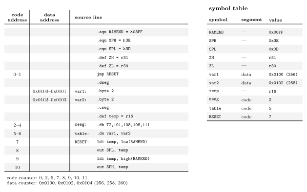
Figure 28: Pass one over the example, line by line. The two address columns show where each line is placed in its own segment, so a range means the line takes several words or bytes: the jmp two words, the 5-byte .db three words with its pad, the .dw two words, each .byte 2 two bytes. Lines that only name something or switch segment take no space and have no address. The code and data counters advance independently, which is why mesg comes straight after the jmp even though the data lines sit between them in the file. On the right is the symbol table pass one leaves behind: every name, the segment its value belongs to, and the value. The .equ and .def names have no segment.
So the instruction at RESET is at program address 7, mesg is at 2, table at 5, and the variables at 256 and 258.
Only one reference in the program is forward: jmp RESET. Every other symbol (RAMEND, var1, var2, mesg, SPL, SPH, ZH, ZL, temp) is defined above the line that uses it. One is enough to need the second pass.
Worked: what pass two writes
With the table complete, pass two replaces every symbol by its value and encodes:
| Address | Statement | With symbols replaced | Machine word(s) |
|---|---|---|---|
| 0–1 | jmp RESET |
jmp 7 |
0x940C 0x0007 |
| 2–4 | .db 72,101,108,108,111 |
bytes 72, 101, 108, 108, 111 and a pad 0 | 0x6548 0x6C6C 0x006F |
| 5–6 | .dw var1, var2 |
.dw 0x0100, 0x0102 |
0x0100 0x0102 |
| 7 | ldi temp, low(RAMEND) |
ldi r16, 0xFF |
0xEF0F |
| 8 | out SPL, temp |
out 0x3D, r16 |
0xBF0D |
| 9 | ldi temp, high(RAMEND) |
ldi r16, 0x08 |
0xE008 |
| 10 | out SPH, temp |
out 0x3E, r16 |
0xBF0E |
| later | ldi ZH, high(mesg*2) |
ldi r31, 0x00 |
0xE0F0 |
| later | ldi ZL, low(mesg*2) |
ldi r30, 0x04 |
0xE0E4 |
| later | lpm |
lpm |
0x95C8 |
Points worth checking by hand:
ldi r16, 0xFF. The form is1110 KKKK dddd KKKK, withddddthe register number minus 16.K=1111 1111anddddd=0000, so1110 1111 0000 1111=0xEF0F.- The
.dbwords. The first byte of each pair is the low byte: 72 and 101 make0x6548. The odd fifth byte, 111 =0x6F, shares its word with the pad. low()andhigh()split a 16-bit value into its bytes at assembly time.RAMEND=0x08FFgives0xFFand0x08: this is the stack pointer being set to the top of SRAM (procedures-and-the-stack).mesg*2.mesgis a word address, 2.lpmreads one byte of program memory from the byte address in Z, and word 2 starts at byte 4. So Z =0x0004, andlpmloadsr0with the byte there, 72, theHofHello. The two kinds of address are drawn in memory-models.tableholds the two variables’ addresses,0x0100and0x0102: a table of pointers, in flash, into the data segment.
Common mistakes
- Counting
jmpas one word. It is two, because it carries a full program address (avr-branches-and-jumps).rjmpis one. - Forgetting the pad. A
.dbline with an odd number of bytes takes a whole extra word, and each line is padded separately. - Counting
.dbbytes as words. Two bytes share a word in program memory. - Letting
.dseglines move the code counter, or the other way round. Each segment has its own counter, and switching segments only chooses which one is in use. - Giving size to lines that only name things.
.equ,.set,.def,.cseg,.dseg,.includeand comments place nothing. - Expecting
.byteto store a value..byte 2reserves two bytes. It does not put a 2 anywhere. Constants go in flash or EEPROM with.dbor.dw. .deffor a constant, or.equfor a register..defis for registers only.- Redefining an
.equ. It cannot be changed; that is what.setis for. - Handing a code label straight to
lpm. A code label is a word address.lpmwants the byte address, the label times 2. - Ending statements with a semicolon out of habit from another language. In AVR assembly it starts a comment.
- Assuming another assembler reads the same way. Directive names and meanings change between assemblers, even for the same chip.
See also
- avr-program-structure — the skeleton: vector table,
RESET, the main loop, and where segments and directives go in it - memory-models — word and byte addresses, cell sizes, and the AVR’s separate address spaces
- avr-architecture — flash, SRAM and EEPROM, the three memories behind the three segments · memory-technologies — what each of the three is as a technology
- avr-instructions · avr-branches-and-jumps — instruction sizes, which decide how far the code counter moves
- avr-interrupts —
.orgplacing eachjmpin the vector table - procedures-and-the-stack — the stack pointer set-up the worked example starts with
- instruction-set-architecture — assembly as a level, one line to one instruction
- compilation-and-linking — the road to machine code from C
- 2026-10-08-assembly-process — Lecture 20
AVR Architecture
The Atmel AVR: what is on the chip, how the CPU is laid out, and where the fetch-decode-execute cycle happens in it. See cpu-organisation for the generic picture this specialises and avr-instructions for what it executes.
Microcontroller, not microprocessor
Atmel AVR devices are microcontrollers. A microcontroller includes lots of components on one chip:
- CPU
- Memory (RAM)
- Program memory
- Input/output devices
That is the distinction from a microprocessor, which is the CPU alone. An ATmega324A is not a CPU — it contains a CPU, alongside memory and a large collection of peripherals, so that a useful system can be one chip rather than a board full of them.
The AVR CPU
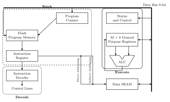
Figure 29: The AVR CPU core, with the three stages of the cycle marked. Fetch (dashed) reads the next instruction from flash under the program counter into the instruction register; decode (dotted) turns it into control lines; execute (solid) runs it over the register file, ALU and status register, with the 8-bit data bus tying everything together. The two lines dropping to the Data SRAM are the direct and indirect addressing routes — both come out of the instruction, which is why they leave from the instruction register. The execute group takes in the status register, the register file and the ALU; the Data SRAM sits outside it.
Reading the diagram as the cycle of fetch-decode-execute-cycle:
| Stage | Blocks involved |
|---|---|
| Fetch | Program Counter → Flash Program Memory → Instruction Register |
| Decode | Instruction Register → Instruction Decoder → Control Lines |
| Execute | General purpose registers → ALU → back to registers, with Status and Control updated |
Because these three groups are largely separate hardware, the AVR overlaps them: while one instruction executes, the next is being fetched. This course calls it a three-stage pipeline. The ATmega164A/324A/644A/1284P datasheet describes the core as “single level pipelining”, i.e. fetch and execute overlapping, which is two stages. Answer three-stage pipeline in the exam, but the datasheet is the authority on the hardware.
The pieces
| Block | Notes |
|---|---|
| Flash program memory | Holds the program. 32 kB on the ATmega324A, and non-volatile — it survives power loss |
| Program Counter | Addresses flash to select the next instruction — the PC of cpu-organisation |
| Instruction Register | Holds the instruction currently being worked on |
| Instruction Decoder | Turns the instruction’s bits into control lines — this is the control unit |
| 32 × 8 general purpose registers | R0–R31, each 8 bits wide, built from flip-flops |
| ALU | 8-bit, so AVR is an 8-bit machine |
| Status and Control | Holds the flags the ALU produces — N, Z, C, V among others |
| Data SRAM | 2 kB, volatile — static RAM, i.e. flip-flops |
| Data bus | 8 bits wide, tying the execute-side blocks together |
Two addressing routes reach the SRAM, drawn as the two vertical paths in Figure 29 — direct addressing (the address is in the instruction) and indirect addressing (the address is in a register). Both leave from the instruction register, because in either case it is the instruction that says which cell is wanted; they differ only in whether it says so with a literal address or with the name of a pointer. Both, and the other two modes, are in addressing-modes.
Four numbers define the chip: the flash is 32 kB and non-volatile; the SRAM is 2 kB, volatile, and made of static flip-flops; the register file is 32 registers, r0…r31, each 8 bits wide and made of flip-flops; and the ALU is 8-bit, which makes the AVR an 8-bit machine.
The register file
General purpose registers (0–31) are quite regular and can be used interchangeably. Two exceptions are worth having by heart:
- A few instructions work on half the registers (r16–r31), because only 4 bits are used to represent the operand in the instruction and \(2^4 = 16\).
LDI,SER,ANDI,ORIandCPIare among them — see avr-instructions. - X, Y and Z are register pairs that double as 16-bit pointers.
X, Y and Z
The top six registers of the file are those three pairs, low byte in the lower-numbered register:
| Pointer | High : Low | Register addresses |
|---|---|---|
| X | R27 : R26 | 0x1B : 0x1A |
| Y | R29 : R28 | 0x1D : 0x1C |
| Z | R31 : R30 | 0x1F : 0x1E |
Two 8-bit registers side by side make a 16-bit address — which is what the data space needs and no single 8-bit register can hold. They are what indirect addressing uses: ld r5, X means “load from wherever X points”, and the instruction only has to name which pointer, so it stays one word (addressing-modes).
The low byte living in the lower-numbered register is the same little-endian convention the AVR uses in memory (memory-models).
Address spaces
The AVR is a Harvard machine — separate address spaces for instructions and data — so 0x0000 names two entirely different locations depending on which space is meant, and the instruction decides.
Data address space — 0x0000 to 0x08FF
| Region | Addresses | Size |
|---|---|---|
| 32 Registers | 0x0000–0x001F |
32 |
| 64 I/O Registers | 0x0020–0x005F |
64 |
| 160 Ext I/O Reg. | 0x0060–0x00FF |
160 |
| Internal SRAM | 0x0100–0x08FF |
2048 bytes (2 kB) |
The register file and all 224 I/O registers are mapped into the data space, ahead of the SRAM. That is what lets lds/sts reach an I/O register by its data address while in/out reach the first 64 by their I/O register number — the two numbering systems differ by exactly the 0x20 the register file occupies. Details in avr-io-ports.
The datasheet draws the SRAM box as 1024/2048/4096/16384 × 8 because the diagram covers the whole ATmega164A/324A/644A/1284P family; the 324A is the 2048 entry, which is what puts the top of the data space at 0x08FF.
Program memory — 0x0000 to 0x3FFF
\(2^{14}\) 16-bit words: 16,384 instruction words = 32,768 bytes = 32 kB. The datasheet splits it into an Application Flash Section and, at the highest addresses, a Boot Flash Section.
0x3FFF \(= 2^{14} - 1\), and the sizing arithmetic — why 32 kB of program memory is 14 address bits rather than 15 — is worked through in memory-models. The short version: the cells are 16 bits wide, so there are half as many of them as there are bytes.
The AVR status register
8 bits, all readable and writable, all reset to 0:
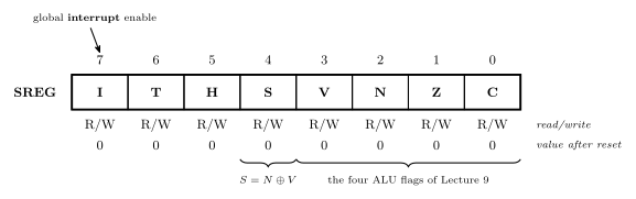
Figure 30: The status register, in the three-row form the datasheet uses: bit numbers above, flag names in the boxes, then the access row and the value each bit takes after reset. The callout names bit 7, the global interrupt enable; the braces underneath mark the four ALU flags and the sign flag \(S = N \oplus V\).
Instruction descriptions refer to these as SREG(n) by bit number:
| Flag | Bit | Meaning |
|---|---|---|
| C | SREG(0) | carry — was a carry out generated? |
| Z | SREG(1) | zero — was the result 0? |
| N | SREG(2) | negative — the sign bit of the result |
| V | SREG(3) | overflow — did a two’s complement addition/subtraction overflow? |
| S | SREG(4) | sign, \(= N \oplus V\) — the sign of the result corrected for any overflow |
| H | SREG(5) | half-carry — carry out of bit 3 |
| T | SREG(6) | transfer bit, used by BLD and BST |
| I | SREG(7) | global interrupt enable — set by sei, cleared by cli; cleared by the hardware when it takes an interrupt and set again by reti (avr-interrupts) |
C, Z, N and V are exactly the four flags of fetch-decode-execute-cycle.
S is not simply “the sign bit” — that is N. \(S = N \oplus V\) means: the result is negative (with no overflow), or would have been negative had overflow not occurred. That correction is what makes signed comparisons work, which is why the signed branches (BRLT, BRGE) test S while the unsigned ones (BRLO, BRSH) test C. The four cases — including the overflow case where N alone gives the wrong answer — are drawn in 2026-09-14-flow-of-control, and the branch pairs are tabulated in avr-branches-and-jumps.
The one-line meanings and the SREG(n) numbering are those of Atmel’s AVR Instruction Set Manual and the instruction summary in the ATmega324A datasheet. The I/O register map is the I/O register summary, pages 636–639 of the ATmega164A/324A/644A/1284P datasheet, which writes the I/O register number first and the data memory address in parentheses after it.
On-chip peripherals (ATmega324A)
Beyond the CPU and its memories, the chip carries a large set of peripherals — this is what makes it a microcontroller rather than a processor. The two figures nest: the whole of Figure 29 is what sits inside the single box marked AVR CPU in Figure 31.
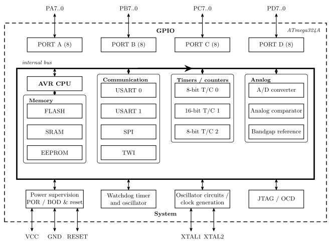
Figure 31: What is on the ATmega324A: the datasheet block diagram, rearranged into clusters by kind of thing — GPIO, memory, communication, timers/counters, analog and system. The dashed outline is the package boundary and the heavy rectangle inside it the internal bus, both as the datasheet draws them; the individual peripheral-to-port wiring is left out.
| Group | On the chip |
|---|---|
| General purpose I/O | PORT A, PORT B, PORT C, PORT D — four 8-bit ports |
| Communication | USART 0, USART 1, SPI, TWI |
| Timers/counters | 8-bit T/C 0, 16-bit T/C 1, 8-bit T/C 2 (T/C 3 is on the ATmega1284/1284P, not the 324A — the family datasheet’s block diagram covers both) |
| Analog | A/D converter, analog comparator, internal bandgap reference |
| Memory | Flash (program), SRAM (data), EEPROM (data, non-volatile) |
| System | Power supervision (POR/BOD & reset), watchdog timer and oscillator, oscillator/clock generation (XTAL1, XTAL2), JTAG/OCD |
There are three memories with three different jobs: flash for the program, SRAM for volatile working data, and EEPROM for data that must survive a power cycle. SRAM and EEPROM are the pair to keep straight: both hold data, and they differ only in surviving a power cycle.
See also
- cpu-organisation · fetch-decode-execute-cycle · instruction-set-architecture
- avr-instructions — the instruction set this hardware runs
- avr-io-ports — the I/O registers and the four GPIO ports
- avr-interrupts — the I bit, the vector table and the peripherals’ interrupt sources
- avr-timers-and-counters · avr-usart · avr-spi · analog-to-digital-conversion — four of the peripherals in detail
- memory-models · addressing-modes — the two address spaces, and how instructions name them
- assembly-process — flash, SRAM and EEPROM as the assembler’s three segments
- memory-technologies — flash, SRAM and EEPROM as technologies, and what the boot loader section is for · memory-hierarchy-and-cache — where the registers and SRAM sit by speed, and why the AVR needs no cache
- binary-number-representations — the flags’ two’s complement interpretation
- 2026-08-27-avr-introduction — Lecture 10
- 2026-08-31-instruction-set-architecture-part-1 — Lecture 11
AVR Branches and Jumps
How an AVR program’s control leaves the straight line: the ten conditional branches and which status flag each one reads, why greater than needs two different instructions for signed and unsigned bytes, the three unconditional jumps and how far each can reach, and the assembly idioms — if, if … else, counted and conditional loops — built from them. First met in 2026-09-14-flow-of-control, with the compare instructions and breq/brne first met in 2026-09-03-instruction-set-architecture-part-2. Procedure calls, the other way control moves, are in procedures-and-the-stack.
Flow of control
The flow of control is the sequence in which instructions actually execute. By default it is linear: every fetch-decode-execute cycle ends with \(PC \leftarrow PC + 1\) (fetch-decode-execute-cycle), so the next instruction is the next one in memory. Four kinds of instruction replace that increment with a new value:
| Decides | ||
|---|---|---|
| Branches | conditional | a status-register flag |
| Jumps | unconditional | nothing — always taken |
| Procedure calls and returns | unconditional, and they remember where they came from | procedures-and-the-stack |
| Interrupts / traps | triggered by hardware, not by an instruction | polling-and-interrupts · avr-interrupts |
Everything below is one instruction that writes the PC.
Conditional branches
A conditional branch tests one bit of the status register (avr-architecture) and, if the bit has the value the instruction wants, loads the PC with the address of a label; otherwise execution falls through to the next instruction. There is one instruction per flag per value:
| Branch if flag = | C | N | V | S = N ⊕ V | Z | T | H | I |
|---|---|---|---|---|---|---|---|---|
| 0 | brsh (= brcc) |
brpl |
brvc |
brge |
brne |
brtc |
brhc |
brid |
| 1 | brlo (= brcs) |
brmi |
brvs |
brlt |
breq |
brts |
brhs |
brie |
The first five columns are the ten branches counted above; the last three are the same pattern applied to the remaining flags and are in the instruction set reference. The mnemonics read as the condition, not the flag: brsh is branch if same or higher and happens to be branch if carry clear; brge is branch if greater or equal and happens to be branch if S clear. Learn them as conditions and the flags take care of themselves.
Every branch is relative and short. The offset is seven bits, so a conditional branch can reach only about 64 words either side of itself. For a farther target, branch on the opposite condition around a jmp:
    cp   r5, r6
    brne skip          ; opposite of the condition wanted
    jmp  far_away      ; taken only when r5 == r6
skip:
A taken branch costs two cycles, a not-taken one; the branch itself is one 16-bit word.
Setting the flags first
A branch reads flags; something has to have written them. Usually that is a compare (avr-instructions):
| Computes | Keeps | |
|---|---|---|
cp rd, rr |
rd − rr |
flags only |
cpi rd, K |
rd − K |
flags only — rd must be r16–r31 |
tst rd |
rd AND rd |
flags only — Z and N say whether rd is zero or negative |
but any ALU instruction sets flags, and a branch straight after an add, sub, dec or andi tests the result of that. dec r17 followed by brne loop is the standard loop counter, and no cp is needed. The rule from avr-program-structure holds either way: nothing that disturbs the flag may sit between the setter and the branch.
Signed and unsigned comparisons
Equality is the same question for signed and unsigned bytes, so breq and brne serve both. Ordering is not: whether 1111 1111 is bigger than 0000 0001 depends on whether it means 255 or −1, and the bits alone cannot say (binary-number-representations). The cp sets the same flags either way; the programmer chooses which pair of branches to read them with, and thereby declares the type:
Branch if rd ≥ rr |
Branch if rd < rr |
Reads | |
|---|---|---|---|
| unsigned | brsh — same or higher |
brlo — lower |
C: an unsigned subtraction needs a borrow exactly when the result went below zero |
| signed | brge — greater or equal |
brlt — less than |
S = N ⊕ V: the sign of the result, corrected for overflow |
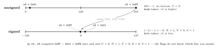
Figure 32: The same two bit patterns on the two number lines an 8-bit register can be read against. As unsigned values, 0xFF is 255 and sits at the far right, above 0x01; as two’s complement values it is \(-1\) and sits just left of zero, below 0x01. One cp r5, r6 produces one set of flags for both readings. The unsigned branches take their answer from the carry flag, which records whether the subtraction had to borrow; the signed branches take theirs from S, which is the sign of the difference with any overflow undone. Choosing brsh or brlt after the compare is the only place the program says which line it meant.
Why S and not N. N is the top bit of the 8-bit result. When a signed subtraction overflows — a large positive minus a large negative, say — the true difference does not fit in 8 bits, the stored result wraps, and its top bit is the opposite of the true sign. V is set in exactly that case. So \(S = N \oplus V\) is the true sign whether or not overflow happened, and one flag test decides < correctly across the whole range; the four cases are drawn in 2026-09-14-flow-of-control. In C none of this is visible: the compiler reads the variable’s declared type and emits brlo for unsigned char and brlt for char, the same way it picks lsr or asr for >> (c-operators).
Unconditional jumps
| Instruction | Target | Size | Cycles | Reach |
|---|---|---|---|---|
jmp label |
absolute address | 32-bit (two words) | 3 | anywhere in program memory |
rjmp label |
PC + signed offset | 16-bit | 2 | ±2 K words (12-bit offset, −2048 to +2047) |
ijmp |
the address held in Z | 16-bit | 2 | anywhere; the target is a run-time value |
jmp carries a full program-memory address — 14 bits for the ATmega324A’s 16 K words of flash — which does not fit beside an opcode in one 16-bit word, so it takes two words and an extra cycle. rjmp carries a 12-bit offset from the instruction’s own position in one word, one cycle less, and reaches ±2 K words; in a program of a few hundred instructions every jump is within range, and it is the normal choice. ijmp takes the destination from Z, the pointer register of addressing-modes, so a program can compute where to go — a jump table, or C’s switch. The assembler resolves labels to addresses or offsets for all three; the programmer writes the label.
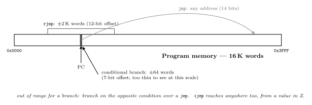
Figure 33: How far each kind of jump can reach from the instruction executing it. Program memory is the ATmega324A’s 16,K words; the marker is the current PC. A conditional branch carries a 7-bit offset and reaches about 64 words either way, an rjmp carries a 12-bit offset and reaches 2,K words either way, and a jmp carries the whole 14-bit address and reaches anywhere. The three are drawn to scale against the memory: the branch window is a sliver, the rjmp window covers a quarter of the chip, and the labs’ programs never leave either. The narrower the reach, the shorter and faster the instruction.
The idioms
Every C control structure (c-control-flow) compiles to a handful of these shapes. The branch is always on the opposite of the source condition, because what the branch does is skip the body.
if:
    cp   r5, r6
    brlt endif         ; skip the body when r5 < r6 (signed)
    ...                ; body: runs when r5 >= r6
endif:
if … else — the else part is the code the branch does not skip, and it needs a jmp past the if part:
    cp   r5, r6
    brge then
    ...                ; else part
    rjmp endif
then:
    ...                ; if part
endif:
while — test at the top, jump back at the bottom:
loop:
    cp   r5, r6
    brsh done          ; exit when r5 >= r6 (unsigned)
    ...                ; body
    rjmp loop
done:
Counted loop — count down to zero so the decrement sets Z for free:
    ldi  r17, 10       ; ten times
loop:
    ...                ; body
    dec  r17           ; sets Z when r17 reaches 0
    brne loop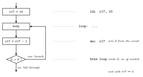
Figure 34: A counted loop, as a flowchart and as the four instructions that implement it. The counter is loaded once; the body runs; the decrement both updates the counter and sets the zero flag from the result; brne reads that flag and either returns to the label or falls out. Counting down rather than up saves the compare: dec leaves Z = 1 exactly when the counter has reached zero, so the branch tests the arithmetic directly. The body executes ten times, with r17 holding 10 down to 1 inside it and 0 on exit — the assembly form of for (i = 10; i != 0; i--).
Picking the branch. Write the C condition, decide signed or unsigned, and take the opposite instruction from the table:
| Source condition | Unsigned: skip with | Signed: skip with |
|---|---|---|
a == b |
brne |
brne |
a != b |
breq |
breq |
a < b |
brsh |
brge |
a >= b |
brlo |
brlt |
a > b |
swap operands: cp b, a then brsh |
cp b, a then brge |
a <= b |
cp b, a then brlo |
cp b, a then brlt |
There is no greater than branch; a > b is b < a, so compare the other way round.
See also
- avr-program-structure — labels, the template, and compare-then-branch drawn out
- procedures-and-the-stack —
call,rcall,icallandret: the jumps that come back - polling-and-interrupts — the fourth way the PC leaves its sequence, with no instruction asking
- avr-instructions —
cp,cpi,tst,dec, and which flags each instruction sets - avr-architecture — the status register; \(S = N \oplus V\)
- c-control-flow — the same shapes in C · binary-number-representations — signed and unsigned bytes
- assembly-process — how the assembler gives a label its address, counting each
jmpas two words - 2026-09-14-flow-of-control — Lecture 15 · 2026-09-03-instruction-set-architecture-part-2 — Lecture 12
AVR Instructions
The AVR instructions introduced so far, in assembly and in machine code. See instruction-set-architecture for what an instruction set is and avr-architecture for the hardware that runs these.
The full alphabetical instruction set — each mnemonic with its operation, description, flags affected, clock count, opcode pattern and an example — is in the AVR instruction set reference: Atmel’s AVR Instruction Set Manual, and the instruction summary in the ATmega324A datasheet the course says to keep open. The notation key immediately below and the per-instruction flag table at the end are unverified against that reference — check them against your own copy before leaning on them.
Reading the instruction set reference
Operand notation — how an operand’s allowed values map onto opcode bits:
| Notation | Meaning | Values | Opcode pattern |
|---|---|---|---|
Rd |
destination register (may be a source too) | r0…r31 | ddddd |
| r16…r31 | dddd (register number − 16) |
||
Rr |
source register | r0…r31 | rrrrr |
Rh:Rl |
register pair as a 16-bit quantity | r25:r24 / X / Y / Z | dd (00 / 01 / 10 / 11) |
K |
constant data | 0…255 | KKKKKKKK |
k |
constant address | −64…63, −2048…2047, 0…65535 | kkkkkkk … kkkk kkkk kkkk kkkk |
b |
bit number in a register | 0…7 | bbb |
s |
bit in the status register | 0…7 | sss |
P |
I/O register number | 0…63 | PPPPPP |
q |
displacement for direct addressing | 0…63 | qqqqqq |
The Rd row is the whole story behind LDI’s restriction — an instruction spending five bits on the register gets all 32; one spending four gets sixteen, and pays for it by starting at r16.
Operation notation — used in the Operation column:
M[a] / PM[a] / IO[a] |
SRAM cell / program memory (flash) byte / I/O register at address a |
PC / SP / STACK |
program counter / stack pointer / M[SP] |
← |
assigned value |
reg(a) |
bit a of register reg, numbered 7…0 most to least significant |
Flag names in the Flags Affected column are the SREG bits of avr-architecture.
Register conventions
Two operand names recur throughout the instruction set:
rd— the destination register.rr— the source register.
AVR is a two-operand machine: the destination is also one of the sources, so add rd, rr means rd ← rd + rr. (Contrast a three-operand ISA such as ARM, where add rd, r1, r2 leaves both sources untouched.) This matters when reading code — an AVR arithmetic instruction always overwrites one of its inputs.
Instructions by type
The instruction set can be cut two ways.
By what the instruction touches — the instruction-type list of instruction-set-architecture, filled in with the instructions so far:
| Type | Does | AVR so far |
|---|---|---|
| Input/Output | communicate with I/O devices/ports | IN, OUT |
| Load/Store | move data from/to memory | LD, LDS, ST, STS |
| Move | copy data between registers | MOV |
| Arithmetic | addition, subtraction, … | ADD, ADC, SUB, INC, NEG |
| Logical | Boolean operations | AND, ANDI, OR, ORI, EOR, COM |
| Branching | deciding which instruction to perform next | JMP, BREQ, BRNE |
By operand count, which splits the arithmetic and logical group instead:
| AVR examples | ||
|---|---|---|
| Dyadic | combine 2 operands to produce a result | add r5, r6 (arithmetic) · and r5, r6 (logical, bitwise) |
| Monadic | one operand → one result | ser r16 (set) · clr r5 (clear) · neg r5 (2’s complement) · com r5 (1’s complement) · the shifts and rotates |
The second cut is the one that predicts the syntax: a dyadic instruction has a comma in it, a monadic one does not.
The instructions so far
| Instruction | Meaning | Example |
|---|---|---|
MOV rd, rr |
copy contents of rr into rd — rd ← rr |
mov r3, r14 |
ADD rd, rr |
add contents of rr to rd — rd ← rd + rr |
add r5, r6 |
ADC rd, rr |
add with carry — rd ← rd + rr + C |
adc r11, r5 |
AND rd, rr |
bitwise AND, result into rd |
|
OR rd, rr |
bitwise OR, result into rd |
|
EOR rd, rr |
bitwise exclusive-OR, result into rd |
|
INC rd |
rd ← rd + 1 |
inc r22 |
LDI rd, number |
load immediate — put the number into rd |
ldi r16, 73 |
SER rd |
set all bits — rd ← $FF. Same as ldi rd, 0xFF, so r16–r31 only |
ser r17 |
CLR rd |
clear all bits — rd ← 0. Same as eor rd, rd, so any register |
clr r3 |
SUB rd, rr |
rd ← rd − rr |
sub r7, r19 |
COM rd |
one’s complement — flip all bits | com r8 |
NEG rd |
two’s complement — negate | neg r9 |
ANDI rd, K |
bitwise AND with a constant — r16–r31 only | andi r16, 0x01 |
ORI rd, K |
bitwise OR with a constant — r16–r31 only | ori r16, 0xF0 |
MOV is named misleadingly: it copies, it does not move. The source register is unchanged. It also affects no flags, which is what makes it safe to shuffle values between operations without disturbing the status register.
SER and CLR are short-hand ways of setting/clearing all bits of a register, and their restrictions differ because their expansions do:
| Exactly the same as | Reaches | |
|---|---|---|
ser rd (set register) |
ldi rd, 0xFF |
r16–r31 only — it inherits LDI’s four-bit register field |
clr rd (clear register) |
eor rd, rd |
any register, r0–r31 — EOR is a two-register instruction with five bits for each |
So clr r3 is legal and ser r3 is not, which looks arbitrary until you look at what each one assembles to. clr is also the reason \(X \oplus X = 0\) from bit-masking is worth remembering: XORing a register with itself is how the machine zeroes one.
Compare instructions
These do the arithmetic, discard the result, and keep only the flags — which is exactly what a conditional branch needs.
| Instruction | Does | Note |
|---|---|---|
CP rd, rr |
rd − rr |
compares two registers |
CPI rd, K |
rd − K |
compares against a constant — like ldi, r16–r31 only |
TST rd |
rd AND rd |
examines one register; literally the same operation as and rd, rd |
tst looks odd until you notice that ANDing a value with itself leaves it unchanged (\(X \cdot X = X\)) but still sets N and Z from it — so it is a zero/sign test that costs nothing and clobbers nothing. See bit-masking.
A comparison is the same as subtraction, with the result not saved — it exists only to set status register flags (Z, N, C, V …). And the instruction reference specifies which status register bits are set by which instructions: the flags are defined per instruction rather than falling out of one shared adder, which is the point of the table at the end of this note.
Branch instructions
Based on status register values — the flags a compare just set:
Branches to label if |
|
|---|---|
BREQ label |
Z = 1 |
BRNE label |
Z = 0 |
Together with CP that is a complete conditional: compare, which sets Z exactly when the two operands were equal, then branch on Z.
    cp   r5, r6          ; r5 - r6, result thrown away, flags kept
    breq same            ; Z = 1, i.e. r5 == r6
JMP label is the unconditional version — it tests nothing and always goes. Labels, and the program skeleton the branches live in, are in avr-program-structure.
breq/brne are two of ten: there is one branch per status flag per value, and the pairs that matter for ordering are brsh/brlo (unsigned, on C) and brge/brlt (signed, on S) — the full table, and why the signed pair reads S rather than N, are in avr-branches-and-jumps.
Control flow
The instructions that write the PC, and the two stack instructions that go with the calls (avr-branches-and-jumps, procedures-and-the-stack):
| Instruction | Does | Words | Cycles |
|---|---|---|---|
BRxx label |
branch if a flag has the wanted value; reach ±64 words | 1 | 1 (not taken) / 2 (taken) |
JMP label |
PC ← address of label |
2 | 3 |
RJMP label |
PC ← PC + offset; reach ±2 K words | 1 | 2 |
IJMP |
PC ← Z | 1 | 2 |
CALL label |
push the return address, then as JMP |
2 | 4 |
RCALL label |
push the return address, then as RJMP |
1 | 3 |
ICALL |
push the return address, then as IJMP |
1 | 3 |
RET |
pop the return address into PC | 1 | 4 |
PUSH rr |
store rr at SP, SP ← SP − 1 |
1 | 2 |
POP rd |
SP ← SP + 1, load rd from SP |
1 | 2 |
None of these touches the status register except by what the pushed and popped values happen to be; a call between a cp and its branch is safe only if the procedure preserves the flags, which in practice means it is not.
Three more belong to interrupts, and between them they are the only instructions that change the I bit (avr-interrupts):
| Instruction | Does | Words | Cycles |
|---|---|---|---|
SEI |
I ← 1: interrupts enabled | 1 | 1 |
CLI |
I ← 0: interrupts disabled | 1 | 1 |
RETI |
pop the return address into PC, and I ← 1 | 1 | 4 |
RETI is RET plus set I. A handler that ends in RET returns to the right place and leaves interrupts off for good.
Data movement
Data is usually copied, not moved — in every instruction below the source is left alone. What changes is where the two ends are:
| Direction | Called | AVR |
|---|---|---|
| register → register | move | mov |
| memory → register | load | lds, ld |
| register → memory | store | sts, st |
| I/O register → register | input | in |
| register → I/O register | output | out |
Three different places a value can live — a general purpose register, data memory, an I/O register — and a different instruction family for each. The one thing that is genuinely out of reach is SRAM from in/out: P only goes up to 0x3F, so those two never leave the first 64 I/O registers.
Everything else is a question of cost and numbering, not reachability. Because the I/O registers are mapped into the data space (avr-io-ports), lds/sts can reach one — in r16, 0x09 and lds r16, 0x29 both read PIND, the second for two instruction words instead of one. The bug to actually watch for is writing the I/O register number where the data address belongs, or the reverse.
Load and store
| Does | Addressing | Words | Cycles | |
|---|---|---|---|---|
LD rd, X |
rd ← Mem[X] |
indirect — address in the pointer register | 1 | 2 |
ST X, rr |
Mem[X] ← rr |
indirect | 1 | 2 |
LDS rd, k |
rd ← Mem[k] |
direct — 16-bit address in the instruction | 2 (32 bits) | 2 |
STS k, rr |
Mem[k] ← rr |
direct | 2 | 2 |
For example:
    ld   r5, X           ; r5 <- Mem[X]
    st   X, r5           ; Mem[X] <- r5
    lds  r5, 0x20        ; r5 <- Mem[0x20]
    sts  0x20, r5        ; Mem[0x20] <- r5
Both pairs reach the same data space — the difference is only where the address comes from (addressing-modes), and lds/sts pay a second instruction word for spelling it out. X here is the pointer pair of avr-architecture.
In and out
| Does | Words | Cycles | |
|---|---|---|---|
IN rd, P |
rd ← I/O register P |
1 | 1 |
OUT P, rr |
I/O register P ← rr |
1 | 1 |
rd/rr may be any of r0–r31 — unlike ldi, these are not restricted to the top half — and P is an I/O register number 0–63 (0x00–0x3F) or a name from m324Adef.inc. Examples: in r5, 0x26 (I/O register 0x26 is TCNT0) and out PORTD, r6. Full treatment in avr-io-ports.
One word and one cycle makes these the cheapest access on the chip — cheaper than reaching the very same register through lds/sts, which is the whole reason the first 64 I/O registers are special.
Shifts and rotates
Monadic instructions that move every bit one place. They differ only in what arrives at the vacated end and what happens to the bit that falls off — and in all five, the bit that falls off lands in C.
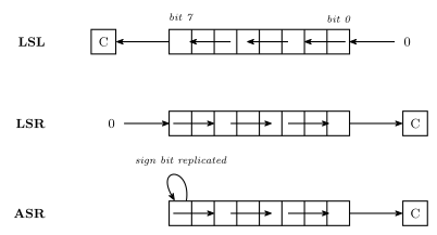
Figure 35: The three shift instructions. LSL and LSR feed a 0 into the vacated end; ASR feeds the sign bit back into itself, which is what makes it a signed division. In all three the bit shifted out lands in the carry flag.
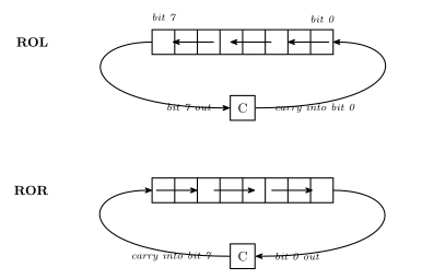
Figure 36: The two rotate instructions. A rotate is a shift whose vacated end is fed from the carry flag instead of a constant, so the register and C together behave as a nine-bit ring.
| Name | Into the vacated end | Out | |
|---|---|---|---|
LSL rd |
Logical Shift Left | 0 → bit 0 |
bit 7 → C |
LSR rd |
Logical Shift Right | 0 → bit 7 |
bit 0 → C |
ASR rd |
Arithmetic Shift Right | bit 7 replicated into itself | bit 0 → C |
ROL rd |
ROtate Left through carry | C → bit 0 | bit 7 → C |
ROR rd |
ROtate Right through carry | C → bit 7 | bit 0 → C |
What they compute
Shifting a binary number one place is multiplying or dividing it by two, which is the whole reason these exist. Using four bits for legibility:
| Worked example | ||
|---|---|---|
LSL |
× 2 | 0010 (2) → 0100 (4) → 1000 (8) |
LSR |
÷ 2, read unsigned | 0110 (6) → 0011 (3); 1000 (8 unsigned) → 0100 (4) |
ASR |
÷ 2, read signed | 1000 (\(-8\)) → 1100 (\(-4\)) |
LSR and ASR are the pair to keep straight. Given 1000, LSR produces 0100 — right if the value meant unsigned 8, wrong if it meant \(-8\). ASR replicates the sign bit into the vacated position and produces 1100 \(= -4\). The same bits go in; the instruction is where you declare which interpretation you meant (binary-number-representations).
There is no matching pair going the other way, because left shifts need no such distinction: a 0 always enters at the bottom, and the signed and unsigned readings of “× 2” agree — right up until the result stops fitting in eight bits.
Shifting a value wider than eight bits
Rotates exist to carry a bit from one byte into the next. To multiply the 16-bit unsigned value in r13:r14 by two (so r13 is the high byte, r14 the low):
    lsl  r14             ; low byte x2; bit 7 falls out into C
    rol  r13             ; high byte x2, pulling C into its bit 0
LSL on the low byte pushes its top bit into C; ROL on the high byte pulls exactly that bit back in at the bottom. The two instructions together shift a sixteen-bit quantity one place.
The wrong answers are worth naming, because each fails differently. lsl r13 (and asl r13, which is the same operation under another name — shifting left, a 0 always enters) shifts the high byte but feeds it a 0, discarding the bit the low byte just produced. rol r14 rotates the wrong byte.
Building wider operations from 8-bit ones
The AVR supports exactly one data type in hardware — an 8-bit integer (instruction-set-architecture). Everything wider is a sequence of instructions, and C is what stitches the pieces together.
Add the 16-bit quantity r5:r4 to r11:r10, result in r11:r10 — high byte named first, so r4 and r10 are the low bytes:
    add  r10, r4         ; r10 <- r10 + r4        (low bytes; carry out lands in C)
    adc  r11, r5         ; r11 <- r11 + r5 + C    (high bytes, plus that carry)
ADD on the low bytes leaves any carry out of bit 7 in C, and ADC on the high bytes adds it back in — the same column-by-column carrying as long addition on paper, one byte per column.
The order is not negotiable, and neither is what sits between the two lines: adc has to run after the add that produced the carry, and any instruction in between that touches C ruins the result. That is the general shape of multi-byte arithmetic on an 8-bit machine — low end first, and nothing allowed to disturb the flag in the middle.
Constants
Constants do not have to be hexadecimal. All five of these load the same value into r17:
| Written | Radix | |
|---|---|---|
ldi r17, 0x34 |
hexadecimal | 0x prefix |
ldi r17, $34 |
hexadecimal | $ prefix |
ldi r17, 52 |
decimal | no prefix |
ldi r17, 064 |
octal | a leading 0 |
ldi r17, 0b00110100 |
binary | 0b prefix |
\(\texttt{0x34} = 52 = 64_8 = \texttt{0b00110100}\). The octal form is the trap: a leading zero changes the radix, so 012 is 10, not 12.
LDI’s restrictions
LDI is the one with strings attached:
- Registers r16 to r31 only. Not r0–r15.
- 8-bit numbers,
00000000to11111111. Written in decimal the range is \(-128\) to \(255\) — that span covers both the signed and the unsigned reading of eight bits.
A counter-example, and the legal version of it:
    ldi  r0, 5           ; NOT legal - r0 is below r16
    ldi  r16, 5          ; the same idea, in a register ldi can reach
The register restriction is not arbitrary: it falls straight out of the encoding below, which has only four bits for the register number.
Machine code
Each instruction is a 16-bit word made of an opcode and operand bit fields — see instruction-set-architecture. In the AVR datasheet’s notation, a format like 0000 11rd dddd rrrr means the literal bits are fixed and each letter is one bit of an operand, gathered from wherever it appears.
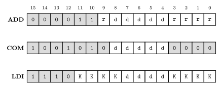
Figure 37: Three AVR instruction encodings, each 16 bits. Fixed opcode bits are shaded; letters are operand bits. In ADD and LDI the operand bits are not contiguous — the register number’s top bit sits apart from the rest, and LDI’s constant is split into two nibbles either side of the register field.
ADD — 0000 11rd dddd rrrr
The opcode is bits 15–10, 0000 11 — six fixed bits, all that is left once the two five-bit register numbers have taken ten of the sixteen. The destination register number is d dddd — five bits, so all 32 registers — and the source is r rrrr. Both have their top bit separated from the other four, and note the order in the middle nibble: the source’s top bit (r, bit 9) comes before the destination’s (d, bit 8), even though the mnemonic writes the destination first.
Worked example: add r23, r7.
| Register | In binary (5 bits) | Split as | |
|---|---|---|---|
rd |
r23 = 16 + 4 + 2 + 1 | 10111 |
d = 1, dddd = 0111 |
rr |
r7 = 4 + 2 + 1 | 00111 |
r = 0, rrrr = 0111 |
Dropping those into 0000 11rd dddd rrrr:
\[\texttt{0000 1101 0111 0111}\]
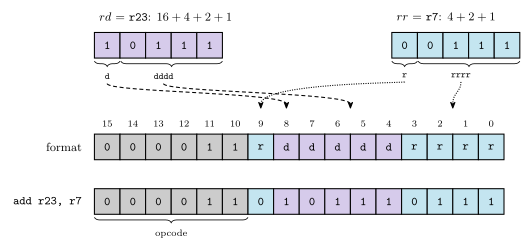
Figure 38: Assembling add r23, r7. Each register number is written as five bits, then torn in two: the top bit goes into the middle nibble and the low four into their own field. Shading, not position, is what tells the two operands apart here. The two guide lines cross because the destination’s bit sits between the source’s two pieces.
COM — 1001 010d dddd 0000
Flip all bits — one’s complement. One register operand, again as d dddd.
Worked example: com r19. r19 = 16 + 2 + 1 = 10011, so d = 1 and dddd = 0011:
\[\texttt{1001 0101 0011 0000}\]
LDI — 1110 KKKK dddd KKKK
Two operand fields:
K— the 8-bit constant, split into two nibbles: the high four bits in the firstKKKKfield, the low four in the last.d— the register number minus 16.
That subtraction is why LDI only reaches r16–r31: the field is four bits, so it can express \(2^4 = 16\) distinct registers, and the ISA spends them on the top half of the register file.
Applying the rule to ldi r16, 73: \(d = 16 - 16 = 0\), so dddd = 0000; \(73 = \texttt{0100 1001}\), so the high nibble is 0100 and the low nibble 1001:
\[\texttt{1110 0100 0000 1001}\]
Flags, by instruction
The reference’s Flags Affected column is worth reading rather than assuming — the flags are defined per instruction, not derived from a single adder. For the instructions above:
| Instruction | Z | C | N | V |
|---|---|---|---|---|
MOV, LDI, SER |
— | — | — | — |
AND, ANDI, OR, ORI, EOR, TST |
from result | unchanged | from result | cleared to 0 |
ADD, ADC, SUB, CP, CPI |
from result | from carry/borrow | from result | signed overflow |
CLR |
always 1 | unchanged | always 0 | cleared to 0 |
COM |
from result | always set to 1 | from result | cleared to 0 |
NEG |
from result | set unless the result is $00 |
from result | set only if the result is $80 |
Two of these will catch you out. The logical operations leave C alone entirely — whatever it held before an and it still holds after. And COM sets C unconditionally, which is not a carry out of anything; it is a defined convention, chosen so that com followed by an increment behaves like a negation.
The CLR row is just the logical row with a result that is guaranteed to be 0x00 — clr rd is eor rd, rd — which makes it the one instruction whose flags you can predict without knowing the operand.
For the shift, rotate and branch instructions, look the flags up in the reference rather than guessing. The one part that is visible in the diagrams above is C: every shift and rotate sets it from the bit that fell out. The rest is defined per instruction, as the paragraph opening this section warns.
For ADD specifically, the manual gives the flags as Boolean formulas over the operand and result bits, writing \(R\) for the result (which equals Rd after the operation):
\[N = R_7 \qquad Z = \overline{R_7}\cdot\overline{R_6}\cdot\overline{R_5}\cdot\overline{R_4}\cdot\overline{R_3}\cdot\overline{R_2}\cdot\overline{R_1}\cdot\overline{R_0}\] \[V = Rd_7 \cdot Rr_7 \cdot \overline{R_7} + \overline{Rd_7}\cdot\overline{Rr_7}\cdot R_7 \qquad C = Rd_7 \cdot Rr_7 + Rr_7 \cdot \overline{R_7} + \overline{R_7}\cdot Rd_7\]
\(Z\) is a NOR over every result bit. \(V\) says overflow happened exactly when both operands had the same sign and the result’s differs — two negatives giving a positive, or two positives giving a negative. And \(S = N \oplus V\), for signed tests. See avr-architecture.
See also
- instruction-set-architecture · avr-architecture · bit-masking
- avr-io-ports — the I/O registers
in/outreach - addressing-modes — the four ways an operand names its value
- avr-program-structure — labels,
jmpand the program skeleton - avr-interrupts —
sei,cli,reti, and which flags an interrupt handler must save - binary-number-representations — one’s and two’s complement, and the \(-128\) to \(255\) range
- 2026-08-27-avr-introduction — Lecture 10
- 2026-09-03-instruction-set-architecture-part-2 — Lecture 12
AVR Interrupts
How the ATmega324A implements interrupts, and how to write one and switch it on, in assembly and in C: the path from a device’s request to the handler and back, the vector table, the switches that decide whether a request is taken, the ISR template and its stack, ISR() and the _vect names, volatile, priority, and a complete timer-interrupt program. First met in 2026-09-21-interrupts. What an interrupt is on any CPU (polling versus interrupts, the fourteen-step sequence, transparency, nesting) is polling-and-interrupts.
The path of an interrupt
An interrupt is a procedure call the hardware makes (procedures-and-the-stack). The CPU finishes the instruction in progress, pushes the address of the next one, turns interrupts off and loads the PC with the address of the vector table entry for the source. The entry holds a jmp to the handler. The handler ends with reti, which pops the return address and turns interrupts back on.
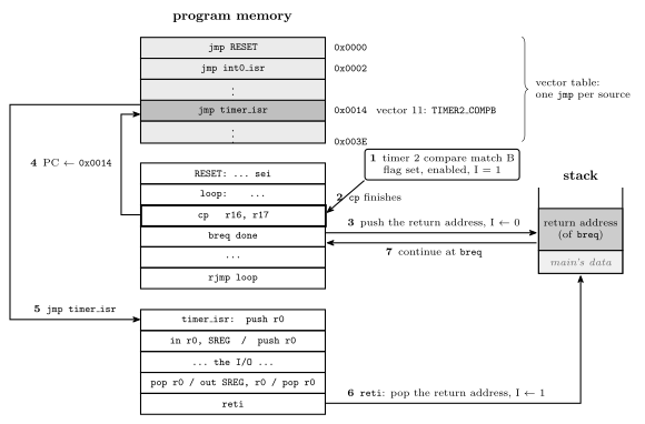
Figure 39: One timer interrupt from start to finish. The request (1) arrives while cp is executing, and the CPU lets it finish (2): an AVR instruction is never abandoned halfway. The hardware then pushes the address of the next instruction, breq, clears the I bit (3), and loads the PC with 0x0014 (4), the vector table entry for Timer/Counter 2 compare match B. The jmp stored there reaches the handler (5), which saves what it uses, does its work, restores, and ends with reti (6). That pops the return address and sets I again, and execution continues at breq (7) as if nothing had happened. It will, provided the handler restored the status register, because breq is about to read the Z flag that cp set. Nothing in the main program refers to the handler; the vector table is the only link between them.
The vector table
The first addresses of program memory hold the interrupt vector table: one entry per interrupt source, in a fixed order, each a two-word jmp to that source’s handler (avr-branches-and-jumps). The AVR uses a table of jump instructions, not a table of addresses. When it takes an interrupt it loads the PC with the address of the entry itself and executes what it finds there. So:
\[\text{entry address} = 2 \times (\text{vector} - 1)\]
RESET is vector 1, at 0x0000. A reset is taken through the same table as an interrupt, which is why every program begins with jmp RESET (avr-program-structure). The table has 31 entries on the ATmega324A and ends at 0x003C, so the program proper starts at 0x003E.
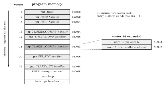
Figure 40: The bottom of program memory. Each vector-table entry is two words, the two halves of a jmp, so entry \(n\) sits at address \(2(n-1)\), and the table’s order is also its priority order: when two requests are waiting, the one nearer the top is taken first. The expanded entry shows what one of them holds, taking vector 14, Timer/Counter 1 compare match A, as the example. An entry for a source the program does not use can hold anything, as long as that interrupt is never enabled. The program itself starts at the first address after the table, which the jmp in entry 1 reaches at reset.
The full table for the ATmega324A, from pages 69–70 of the datasheet. The Group column sorts the sources by kind: GPIO, T/C, Comms, analog and system. The C name is the Source followed by _vect.
| Vector | Address | Source | Interrupt definition | Group | C handler |
|---|---|---|---|---|---|
| 1 | 0x0000 |
RESET |
RESET, watchdog reset, etc. | — | — (the program’s start) |
| 2 | 0x0002 |
INT0 |
External Interrupt Request 0 | GPIO | ISR(INT0_vect) |
| 3 | 0x0004 |
INT1 |
External Interrupt Request 1 | GPIO | ISR(INT1_vect) |
| 4 | 0x0006 |
INT2 |
External Interrupt Request 2 | GPIO | ISR(INT2_vect) |
| 5 | 0x0008 |
PCINT0 |
Pin Change Interrupt Request 0 (port A) | GPIO | ISR(PCINT0_vect) |
| 6 | 0x000A |
PCINT1 |
Pin Change Interrupt Request 1 (port B) | GPIO | ISR(PCINT1_vect) |
| 7 | 0x000C |
PCINT2 |
Pin Change Interrupt Request 2 (port C) | GPIO | ISR(PCINT2_vect) |
| 8 | 0x000E |
PCINT3 |
Pin Change Interrupt Request 3 (port D) | GPIO | ISR(PCINT3_vect) |
| 9 | 0x0010 |
WDT |
Watchdog Time-out Interrupt | system | ISR(WDT_vect) |
| 10 | 0x0012 |
TIMER2_COMPA |
Timer/Counter2 Compare Match A | T/C | ISR(TIMER2_COMPA_vect) |
| 11 | 0x0014 |
TIMER2_COMPB |
Timer/Counter2 Compare Match B | T/C | ISR(TIMER2_COMPB_vect) |
| 12 | 0x0016 |
TIMER2_OVF |
Timer/Counter2 Overflow | T/C | ISR(TIMER2_OVF_vect) |
| 13 | 0x0018 |
TIMER1_CAPT |
Timer/Counter1 Capture Event | T/C | ISR(TIMER1_CAPT_vect) |
| 14 | 0x001A |
TIMER1_COMPA |
Timer/Counter1 Compare Match A | T/C | ISR(TIMER1_COMPA_vect) |
| 15 | 0x001C |
TIMER1_COMPB |
Timer/Counter1 Compare Match B | T/C | ISR(TIMER1_COMPB_vect) |
| 16 | 0x001E |
TIMER1_OVF |
Timer/Counter1 Overflow | T/C | ISR(TIMER1_OVF_vect) |
| 17 | 0x0020 |
TIMER0_COMPA |
Timer/Counter0 Compare Match A | T/C | ISR(TIMER0_COMPA_vect) |
| 18 | 0x0022 |
TIMER0_COMPB |
Timer/Counter0 Compare Match B | T/C | ISR(TIMER0_COMPB_vect) |
| 19 | 0x0024 |
TIMER0_OVF |
Timer/Counter0 Overflow | T/C | ISR(TIMER0_OVF_vect) |
| 20 | 0x0026 |
SPI_STC |
SPI Serial Transfer Complete | Comms | ISR(SPI_STC_vect) |
| 21 | 0x0028 |
USART0_RX |
USART0 Receive Complete | Comms | ISR(USART0_RX_vect) |
| 22 | 0x002A |
USART0_UDRE |
USART0 Data Register Empty | Comms | ISR(USART0_UDRE_vect) |
| 23 | 0x002C |
USART0_TX |
USART0 Transmit Complete | Comms | ISR(USART0_TX_vect) |
| 24 | 0x002E |
ANALOG_COMP |
Analog Comparator | analog | ISR(ANALOG_COMP_vect) |
| 25 | 0x0030 |
ADC |
ADC Conversion Complete | analog | ISR(ADC_vect) |
| 26 | 0x0032 |
EE_READY |
EEPROM Ready | system | ISR(EE_READY_vect) |
| 27 | 0x0034 |
TWI |
2-wire Serial Interface | Comms | ISR(TWI_vect) |
| 28 | 0x0036 |
SPM_READY |
Store Program Memory Ready | system | ISR(SPM_READY_vect) |
| 29 | 0x0038 |
USART1_RX |
USART1 Receive Complete | Comms | ISR(USART1_RX_vect) |
| 30 | 0x003A |
USART1_UDRE |
USART1 Data Register Empty | Comms | ISR(USART1_UDRE_vect) |
| 31 | 0x003C |
USART1_TX |
USART1 Transmit Complete | Comms | ISR(USART1_TX_vect) |
Every timer event the course uses has its own vector. The three units’ compare matches and overflows are vectors 10–19, and a unit’s compare A and compare B are separate sources with separate handlers, just as they have separate flags (avr-timers-and-counters).
When a request is taken
Four things have to be true before a source’s handler runs. The four setup steps (set up the conditions, enable the interrupt, clear its flag, enable globally) arrange for them:
- The conditions for the interrupt are set up, so that the event can happen at all: a timer running in the right mode, or a pin configured to sense an edge.
- That particular interrupt is enabled, by its own bit in an I/O register. There is one bit per source.
- Its flag is set. The hardware does this when the event occurs, whether or not the interrupt is enabled. That is why the third setup step clears the flag before the interrupt is enabled: afterwards only a fresh event can set it, and an event from before the setup does not fire at once. Clearing is done by writing a 1 to the flag’s bit.
- Interrupts are enabled globally: the I bit of the status register is 1.
sei(orsei()in C) sets it.
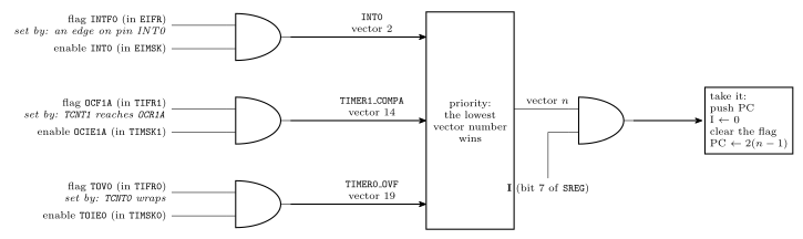
Figure 41: Whether a request becomes an interrupt, drawn as the logic it amounts to. Each source has a flag, set by its event, and an enable bit, set by the program. The source requests an interrupt only while both are 1, and all three sources here are gated the same way. If more than one is requesting, the lowest vector number wins. The winner is taken only if the I bit is also 1, and taking it clears I. For these sources, taking the vector also clears the flag. So a flag with its enable bit off simply stays set, available to be polled, and a flag that goes up while I is 0 waits and is taken the moment I returns to 1.
For the sources the course meets, the bits are:
| Source | Flag (register) | Enable (register) | Conditions set up in |
|---|---|---|---|
INT0 (pin PD2) |
INTF0 (EIFR) |
INT0 (EIMSK) |
EICRA: bits ISC01, ISC00 choose low level 00, any change 01, falling edge 10 or rising edge 11 |
TIMER0_COMPA |
OCF0A (TIFR0) |
OCIE0A (TIMSK0) |
TCCR0A, TCCR0B, OCR0A |
TIMER0_OVF |
TOV0 (TIFR0) |
TOIE0 (TIMSK0) |
TCCR0A, TCCR0B |
TIMER1_COMPA |
OCF1A (TIFR1) |
OCIE1A (TIMSK1) |
TCCR1A, TCCR1B, OCR1A |
TIMER1_OVF |
TOV1 (TIFR1) |
TOIE1 (TIMSK1) |
TCCR1A, TCCR1B |
The naming pattern is regular: an F for the flag and an IE for interrupt enable, with OC for output compare and TOV/TOIE for timer overflow. Each of these flags is cleared automatically when its vector is taken, so a handler does not normally clear its own flag. A program that polls a flag instead, with the interrupt left disabled, must clear it itself (avr-timers-and-counters).
The I bit
| I | Also | |
|---|---|---|
sei |
← 1 | |
cli |
← 0 | |
| taking an interrupt (hardware) | ← 0 | pushes PC, loads the vector address |
reti |
← 1 | pops PC |
I is bit 7 of SREG (avr-architecture), and it is 0 after reset, so no interrupt happens until the program executes sei. Because the hardware clears it on entry, a handler runs with interrupts off unless it turns them back on itself.
External interrupts
An external interrupt is requested by a pin. The ATmega324A has three, each fixed to one pin:
| Interrupt | Pin |
|---|---|
INT0 |
PD2 |
INT1 |
PD3 |
INT2 |
PB2 |
What the pin has to do to make a request is chosen by two sense control bits per interrupt, in EICRA:
ISCn1:0 |
A request is made |
|---|---|
00 |
for as long as the pin is low |
01 |
on any change of the pin |
10 |
on a falling edge, 1 to 0 |
11 |
on a rising edge, 0 to 1 |
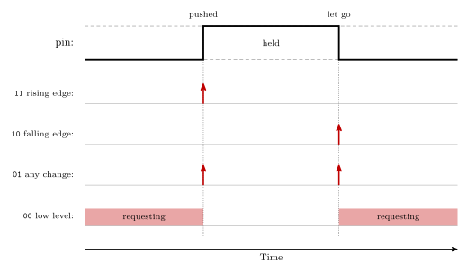
Figure 42: What each sense control setting responds to, for a push button that reads 1 while it is held. A rising edge is the moment the button is pushed and a falling edge is the moment it is let go. Any change gives a request at both. The low level setting is different in kind: it asks for the whole time the pin is low, so the handler runs again and again until the pin goes high.
Setting one up follows the same steps as any other interrupt. For a rising edge on INT0 and a falling edge on INT1:
ISR(INT0_vect) { /* PD2 went from 0 to 1 */ }
ISR(INT1_vect) { /* PD3 went from 1 to 0 */ }

/* in main */
EICRA = (1<<ISC01) | (1<<ISC00) | (1<<ISC11);   /* INT0 rising, INT1 falling */
EIMSK = (1<<INT0) | (1<<INT1);                  /* enable both               */
EIFR  = (1<<INTF0) | (1<<INTF1);                /* clear both flags          */
sei();- Edges fit buttons. An edge happens once per push, however long the button is held. That makes an external interrupt a natural way to act on a push or on a release without the program having to remember what the button was doing last time.
- Bounce. A mechanical contact chatters for a moment as it closes, and each chatter is an edge. One push can then run the handler several times.
- The low level setting keeps asking. If the pin is still low when the handler returns, the interrupt is taken again straight away.
- Priority.
INT0,INT1andINT2are vectors 2, 3 and 4, directly after reset, so they come before every timer and serial interrupt.
Used for the start/stop and reset buttons of a stopwatch in week9-lab-avr-interrupts.
Writing an ISR in assembly
The template:
isr_label:
    push r0              ; save r0: it is about to carry SREG
    in   r0, SREG
    push r0              ; save the interrupted program's flags

    ; ... perform the operation, usually input/output ...
    ; (any other register used: push it here, pop it below)

    pop  r0
    out  SREG, r0        ; flags back as they were
    pop  r0              ; r0 back as it was
    reti                 ; pop PC and set I
SREG cannot be pushed directly, because push takes a general-purpose register. So one register carries it, and that register is saved first. The restore is the save in reverse. Two consequences follow from where the save happens:
- The flags saved are the interrupted program’s. Apart from I, the hardware does not touch them on entry, and
pushchanges none, so the copy is exactly what the interrupted code left. - The saved I bit is 0, because the hardware cleared it before the first instruction of the ISR. Writing the copy back therefore leaves interrupts off until
reti, which is the right moment for them to come back.
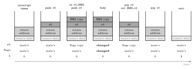
Figure 43: The stack through the ISR template, with the three things the interrupted program relies on (r0, its flags, and the I bit) traced underneath. The hardware’s push of the return address comes first, then the template’s two pushes, the SREG copy on top. The body is free to change r0 and the flags because both are safely on the stack. The restore pops the copy into r0 and writes it to SREG, then pops r0’s own value. When reti runs, the return address is on top again, exactly as the hardware left it. I stays 0 from entry to reti, the copy in the middle included, and it is reti that sets it.
Which registers to save is decided by what the body does. Save any register the body writes. Save SREG if any instruction in the body changes a flag, which rules in arithmetic, logic, compares and shifts but not in, out, ldi, mov, push or pop (avr-instructions). A handler that only copies a port to another port needs one register and no SREG at all (worked in 2026-09-21-interrupts).
Placing the entry in the table
The template in avr-program-structure puts jmp RESET at 0x0000 and leaves a comment where the handlers go. Once a vector is used, its jmp has to sit at exactly that vector’s address. The assembler’s .org directive sets the address of whatever comes next (assembly-process):
.include "m324Adef.inc"

.org 0x0000
        jmp  RESET
.org 0x001A              ; vector 14: TIMER1_COMPA
        jmp  timer1_compa_isr
.org 0x003E              ; first address after the table
RESET:
        ; stack pointer, ports, timer 1, TIMSK1 ...
        sei
loop:
        ; ...
        rjmp loop

timer1_compa_isr:
        push r0
        in   r0, SREG
        push r0
        ; ...
        pop  r0
        out  SREG, r0
        pop  r0
        reti
An assembly program that uses interrupts must also set up the stack pointer before the first sei (procedures-and-the-stack), since taking an interrupt pushes the return address.
Writing an ISR in C
#include <avr/interrupt.h>

ISR(INT0_vect) {
    /* code here */
}
ISR is a macro from avr/interrupt.h, and its argument names the vector: the source name from the datasheet followed by _vect (the table above). From it the compiler does everything the assembly programmer does by hand. The vector table is set up automatically: the handler’s jmp goes in the right entry. Registers are saved and restored automatically, SREG included, and the function ends in reti. What ISR() does not do is any of the four setup steps. In C, as in assembly, the program still sets up the conditions, enables the interrupt, clears its flag and calls sei(). sei() and cli() are macros for the single instructions.
A complete example
Timer 1 in CTC mode, matching eight times a second, with the handler toggling an LED and counting ticks. The timer set-up is Lab 12’s (week8-lab-avr-timers): \(8\,\text{MHz} / (64 \times 15625) = 8\ \text{Hz}\).
#include <avr/io.h>
#include <avr/interrupt.h>

volatile uint8_t ticks = 0;            /* written by the ISR, read by main */

ISR(TIMER1_COMPA_vect) {
    PORTA ^= (1<<0);                    /* toggle the LED on PA0 */
    ticks++;
}

int main(void) {
    DDRA = (1<<0);                      /* PA0 is an output */

    /* 1. conditions: CTC mode, clock/64, match at 15624 */
    OCR1A  = 15624;
    TCCR1A = 0;
    TCCR1B = (1<<WGM12) | (1<<CS11) | (1<<CS10);

    /* 2 and 3. clear any stale match, then enable this interrupt */
    TIFR1  = (1<<OCF1A);
    TIMSK1 = (1<<OCIE1A);

    /* 4. enable interrupts globally */
    sei();

    while (1) {
        if (ticks >= 8) {               /* a second has gone by */
            ticks = 0;
            /* ... once-a-second work ... */
        }
        /* ... anything else: the LED keeps time by itself ... */
    }
}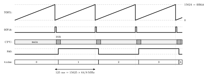
Figure 44: The example program running, one trace per signal. The count climbs to OCR1A = 15624 and is cleared (CTC mode), once every 125 ms. Each match sets OCF1A; the interrupt is enabled and I is 1, so the vector is taken a few cycles later, and taking it clears the flag again. The handler is a sliver of time in which the LED output is toggled and ticks counted, and the rest of the time belongs to main. Nothing in main looks at the timer. The LED blinks at 4 Hz, one toggle per match, however busy main is.
Priority
Priority is determined by vector: the lowest vector is the highest priority. RESET is highest, then INT0, and so on down the table. On the AVR, priority only matters when two or more interrupts are waiting to be serviced, and it decides which is taken first. It never lets one interrupt cut into another’s handler, because I is 0 throughout a handler. The datasheet adds one rule: after reti, the CPU always executes one instruction of the interrupted program before taking the next waiting interrupt, so a stream of interrupts can slow main down but never stop it altogether.
Interrupts can be re-enabled inside a handler with sei. Any incoming or waiting interrupt may then be serviced immediately, nested inside the current handler, even if it has lower priority. Priority plays no part there. Both cases are traced in 2026-09-21-interrupts and set against true priority nesting in polling-and-interrupts.
Pitfalls
- Forgetting
sei(). Everything else is set up, and nothing ever happens, because I is 0 from reset. - Enabling an interrupt that has no handler. In C, avr-libc fills every unused vector with a jump to a default handler that jumps to address 0, so the program restarts whenever the event occurs. It is not a true reset: the I/O registers keep whatever they held, which can make the restart behave differently from a power-up.
- Misspelling the vector name.
ISR(TIMER1_COMPA_Vect)compiles with only a warning, and the handler is never placed in the table, which makes it the previous pitfall. - Not clearing a stale flag before enabling: the interrupt fires once immediately, for an event that happened before the program was ready.
- Clearing a flag with
|=. If the compiler turns it into a read, an OR and a write, it clears every flag in the register that happens to be set (avr-timers-and-counters). Writing just the one bit,TIFR1 = (1<<OCF1A);, is safe however it is compiled. - In assembly: not saving
SREG, unbalanced pushes and pops, orretinstead ofreti. The first corrupts the interrupted code’s flags. The second returns to the wrong address. The third returns correctly but leaves I at 0, so no interrupt ever happens again. - Long handlers. No delay loops and no waiting inside an ISR: every other interrupt waits too, and repeated events of one source merge into one.
- A shared variable without
volatile, or a multi-byte one read withoutcli().
See also
- polling-and-interrupts — polling versus interrupts, the fourteen-step sequence, transparency, nesting policies, traps
- 2026-09-21-interrupts — Lecture 17: the stack revisited, worked questions,
volatiledrawn, priority traced - avr-timers-and-counters — the timer interrupt registers
TIMSKnandTIFRn, and the flags these interrupts replace polling - procedures-and-the-stack — the stack the return address goes on, and initialising
SP - avr-program-structure — the
jmp RESETtemplate the vector table extends - avr-architecture —
SREGand its I bit · avr-instructions — which instructions change the flags - c-preprocessor-and-avr-headers —
volatilein the I/O register macros · bit-masking —(1<<OCIE1A) - week8-lab-avr-timers — Lab 12, the timer set-up the example uses
- week9-lab-avr-interrupts — Lab 14: a stopwatch from a timer interrupt and two external interrupts
- software-timers — one timer interrupt keeping time for the whole program
- avr-usart — the three serial interrupts · analog-to-digital-conversion — the conversion-complete interrupt · avr-spi — the transfer-complete interrupt
AVR I/O Ports
How an AVR program actually reads a switch and lights an LED: the I/O register file, the three registers behind every port, the two instructions that reach them, how to change one bit of a port without disturbing the others, what writing to PINx really does, and the pins’ alternate uses by the serial interfaces. See avr-architecture for the chip these live on, avr-instructions for the instruction set, and io-board for the devices that get wired to the pins.
I/O registers
The ATmega324A has 224 I/O registers — registers that control the peripherals and carry data to and from them:
- Timers and counters
- Analog to digital converters
- Serial input/output
- General purpose input/output ports
They are not the general purpose registers. Some instructions work with these, others with r0–r31, and confusing the two is the standard beginner error — ldi r16, 0xFF and out DDRA, r16 name completely different register files with the same-looking numbers.
Some addresses are reserved (not actually available on this device). The full list is the I/O register summary, pages 636 to 639 of the datasheet.
Where they live, and how you get at them
I/O registers 0 to 223 sit in the data address space at memory addresses 32 to 255 (0x20 to 0xFF) — see memory-models for why the AVR has a separate data space at all. That gives two ways to name the same register, and two names for it:
| Range | Reached by | |
|---|---|---|
| First 64 I/O registers (0 to 63) | data addresses 0x20–0x5F |
in and out and ld/st |
| Other 160 — the “extended” I/O registers (64 to 223) | data addresses 0x60–0xFF |
ld/st only |
so the two numbering systems differ by a constant:
\[\text{data memory address} = \text{I/O register number} + \texttt{0x20}\]
The offset is exactly the 32 general purpose registers, which occupy 0x0000–0x001F at the bottom of the data space ahead of them.
Why the split exists at all: in/out encode the I/O register number in six bits of the instruction word, and \(2^6 = 64\). Everything past register 63 has no room in the encoding, so it can only be reached the long way round, by its data address.
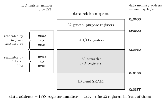
Figure 45: The bottom of the ATmega324A data address space, and the two numbering systems that live on it. Every I/O register has two numbers — its I/O register number (what in/out take) and its data memory address (what ld/st take) — and they differ by a constant 0x20, because the 32 general purpose registers sit in front of them in the same space. Only the first 64 I/O registers have an I/O register number small enough to fit the six operand bits of in/out; the 160 extended ones can be reached by their data address alone. The map follows the convention of csse2010-diagram-notation: lowest address at the top, hex addresses outside.
Extract from the I/O register list
The general purpose port registers are the first twelve entries, in the order PIN, DDR, PORT for each port in turn:
| Data address | I/O reg number | Name |
|---|---|---|
0x2B |
0x0B |
PORTD |
0x2A |
0x0A |
DDRD |
0x29 |
0x09 |
PIND |
0x28 |
0x08 |
PORTC |
0x27 |
0x07 |
DDRC |
0x26 |
0x06 |
PINC |
0x25 |
0x05 |
PORTB |
0x24 |
0x04 |
DDRB |
0x23 |
0x03 |
PINB |
0x22 |
0x02 |
PORTA |
0x21 |
0x01 |
DDRA |
0x20 |
0x00 |
PINA |
Further up the same list, to show the pattern continues and that reserved entries are real:
| Data address | I/O reg number | Name |
|---|---|---|
0x38 |
0x18 |
TIFR3 |
0x37 |
0x17 |
TIFR2 |
0x36 |
0x16 |
TIFR1 |
0x35 |
0x15 |
TIFR0 |
0x34 |
0x14 |
Reserved |
Read the two columns carefully in an exam question. out 0x02, r16 writes PORTA, but sts 0x02, r16 writes general purpose register r2 — the same number, two address spaces, and only the instruction tells them apart.
GPIO ports
The ATmega324A has four 8-bit general purpose I/O ports — PORT A, PORT B, PORT C, PORT D — appearing on the datasheet block diagram as PA7..0, PB7..0, PD7..0 around the edge of the chip, with port C drawn as PC5..0 plus TOSC1/PC6 and TOSC2/PC7 broken out separately — those two pins double as the timer oscillator connections. They are still port C bits, and DDRC/PORTC/PINC still cover all eight.
Three registers are associated with each (x = A, B, C or D):
| Register | Name | What it holds |
|---|---|---|
| DDRx | Data Direction Register | which pins are outputs |
| PORTx | values to output | |
| PINx | values on the pins |
Each is 8 bits — one bit per pin. DDRA0, PORTA0 and PINA0 are the three bits belonging to pin PA0.
What one bit of a port looks like
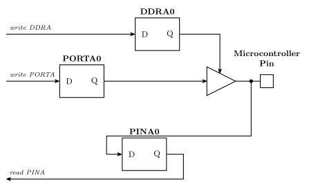
Figure 46: One bit of an AVR port — the three flip-flops behind pin PA0. DDRA0 enables the tri-state buffer, so it decides whether PORTA0’s value is driven onto the pin or the pin is left free for something outside to drive. PINA0 samples whatever is on the pin either way. Hence: DDR is direction, PORT is what you write, PIN is what you read.
1 means output, 0 means input. Writing 0xFF to DDRA makes every bit of port A an output, and writing 0x00 to DDRB makes every bit of port B an input.
Three consequences fall straight out of the circuit:
- PORTx does nothing on a pin whose DDRx bit is 0. The buffer is off; the value sits in the flip-flop unused. (On real AVR hardware it switches an internal pull-up instead.)
- PINx is always live. It samples the pin whether the pin is being driven from inside or outside, so reading PINx on an output pin reads back what you are driving.
- Reading PORTx is not reading the pin. It gives you the value you last wrote. To find out what is there, read PINx — which is why every input example uses
in rd, PINxand neverin rd, PORTx.
in and out
The two instructions that reach the first 64 I/O registers:
| Does | Operands | |
|---|---|---|
in rd, P |
Load I/O register value into general purpose register | rd: r0 to r31. P = I/O register number (0 to 63, 0x00 to 0x3F) or name |
out P, rr |
Store value from general purpose register into I/O register | rr: r0 to r31. P = 0 to 63 (0x00 to 0x3F) or name |
The operand order flips between them, and it flips for a consistent reason: like every AVR instruction, the destination is written first. So the I/O register is the second operand of in and the first of out.
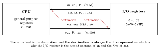
Figure 47: in and out between the two register files: the CPU’s general purpose registers r0–r31 and the first 64 I/O registers. in reads from an I/O register into a general purpose register, out writes the other way, and the head of each arrow, marked destination, is the operand written first. That is why the I/O register is the second operand of in and the first of out.
Answers of the form in DDRB, r16 are the standard trap. What is wrong with them is the mnemonic, not the direction: in’s destination is always one of r0–r31, so it can never be DDRB. Moving a general purpose register into an I/O register is exactly what out does — which is why the right answer in that shape is out DDRB, r16.
in and out reach all 32 general purpose registers, r0–r31 — unlike ldi, they are not restricted to the top half.
Both are one instruction word and one clock cycle, which makes them the cheapest way to touch a peripheral.
Three equivalences, all of them just the number/name table above:
| Written with a number | Same instruction, written with a name |
|---|---|
in r0, 0 |
in r0, PINA |
out 1, r0 |
out DDRA, r0 |
in r5, 0x26 |
in r5, TCNT0 — I/O register 0x26 is timer/counter 0 |
Using port names
Numbers are how the machine sees it; names are how you should write it:
.include "m324Adef.inc"The contents of this file are included directly in the program, and it defines the names for the I/O registers — so DDRA, PORTA, PINA, TCNT0 and the rest can be written instead of 0x01, 0x02, 0x00, 0x26. Everything about the generated machine code is identical; the assembler substitutes the number.
Setting port A (all bits) to be an output, which is the shape of nearly every initialisation block:
    ldi  r16, 0xFF       ; every bit 1 = output
    out  DDRA, r16       ; ... into the direction register
or, using the shorthand of avr-instructions, ser r16 in place of the ldi. Setting a port to be all inputs is the same two lines with 0x00 (or clr), and a mixed port is any other constant — DDRA is a bit pattern like everything else, so ldi r16, 0x0F gives four outputs and four inputs.
Changing one bit of a port
Writing a whole port register is right at initialisation. Afterwards a program usually wants to change one pin and leave the other seven alone, because the other pins belong to other parts of the program. In C that is a read-modify-write with a one-bit mask, the bit named rather than given as a number (bit-masking):
DDRC  |= (1<<5);          /* PC5 becomes an output     */
PORTC |= (1<<5);          /* PC5 driven high           */
PORTC &= ~(1<<5);         /* PC5 driven low            */
PORTC ^= (1<<5);          /* PC5 flipped               */
if (PINC & (1<<2)) { }    /* is PC2 high?              */
In assembly there are two ways:
| Register | Set or clear one bit | |
|---|---|---|
I/O registers 0 to 31, which includes every PINx, DDRx and PORTx |
sbi PORTC, 5 and cbi PORTC, 5 |
one instruction, other bits untouched |
any register in/out reach, 0 to 63 |
in r16, TCCR0B, then ori or andi with the mask, then out TCCR0B, r16 |
three instructions, and a spare register |
sbi and cbi hold the register number in five bits of the instruction, so they reach only the first 32 I/O registers. TCCR0B is I/O register 0x25, 37, which is past them: the long way is the only way. The extended registers past 63, such as TIMSK2 and TCCR1B, need lds and sts in place of in and out.
Writing to PINx
PINx is the port’s input register: reading it gives the levels on the pins. Writing to it is not storing a value. On the ATmega324A, writing a 1 to a bit of PINx toggles the matching bit of PORTx, whatever the pin’s direction, and writing a 0 does nothing.
That makes PINx a quick way to flip a pin:
PINC = (1<<0); /* toggle PC0; the 0s written to the other bits do nothing */and in assembly sbi PINC, 0 does the same in one instruction.
It also makes PINx the wrong register for a clear or a set. PINC &= ~(1<<5) does not clear PC5. If the compiler turns it into a single cbi PINC, 5, it writes a 0 to bit 5 of PINC and nothing happens. If it does a read, an AND and a write, it writes 1s to every other bit that read high, and those pins flip:
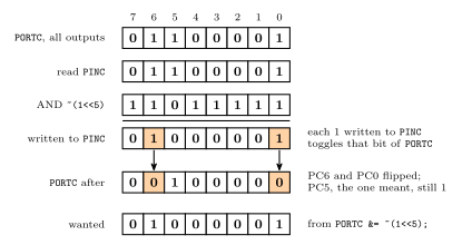
Figure 48: Why a read-modify-write on PINC goes wrong. Port C is all outputs, driving 0110 0001, so its pins read the same. PINC &= ~(1<<5) reads them, clears bit 5 of the reading and writes the result to PINC. A 1 written to a PINx bit is an order to toggle that bit of PORTx, not a value to keep, and a 0 does nothing. So the two other 1s, shaded, flip PC6 and PC0 low, and PC5, the bit meant to be cleared, stays high. The bottom row is what PORTC &= ~(1<<5) would have given.
So: set and clear through PORTx, read through PINx, and write PINx only to toggle.
Alternate pin functions
Most pins have a second job. When the peripheral that owns a pin is switched on, it takes the pin over from the port, and for some pins it overrides DDRx too. The serial interfaces use these:
| Port pin | Package pin | Alternate use | Peripheral |
|---|---|---|---|
| PB0 | 1 | XCK0 | USART0’s clock, used when it is an SPI master |
| PB4 | 5 | \(\overline{\text{SS}}\) | SPI (avr-spi) |
| PB5 | 6 | MOSI | SPI |
| PB6 | 7 | MISO | SPI |
| PB7 | 8 | SCK | SPI |
| PC0 | 22 | SCL | TWI |
| PC1 | 23 | SDA | TWI |
| PD0 | 14 | RXD0 | USART0 (avr-usart) |
| PD1 | 15 | TXD0 | USART0 |
| PD2 | 16 | RXD1 | USART1 |
| PD3 | 17 | TXD1 | USART1 |
| PD4 | 18 | XCK1 | USART1’s clock, used when it is an SPI master |
So the SPI port is the upper half of port B, and the TWI is the bottom two bits of port C. Other pins carry timer outputs, the external interrupts (INT0 and INT1 share PD2 and PD3 with USART1) and, on port A, the analog inputs. A pin can do only one job at a time, so a program that uses the SPI cannot also use PB4 to PB7 as general purpose I/O. The whole pinout is drawn in 2026-10-05-more-io.
Common mistakes
in DDRB, r16.inalways writes a general purpose register. Writing an I/O register isout DDRB, r16.- Reading
PORTxto find out what is on a pin. That gives back what was last written. The pins arePINx. - Setting or clearing a bit through
PINx. A 1 written there toggles, soPINC &= ~(1<<5)flips other pins and leaves PC5 alone. PORTC = (1<<5)to set one pin.=writes all eight bits and drives the other seven low. Use|=.sbiorcbion a register past 31, such asTCCR0B. They cannot reach it; usein,ori/andi,out.- Using a pin as general I/O while its peripheral is on. The SPI, the TWI and the USARTs take their pins over.
See also
- avr-architecture — the data address space these sit in, and the rest of the chip
- avr-instructions · avr-program-structure · bit-masking
- memory-models — why the I/O registers have two addresses
- io-board · device-pinouts — the switches, LEDs and buttons wired to the pins
- week6-lab-avr-io-ports — Lab 10, where this gets wired up
- avr-usart — PD0 and PD1 as a serial port · analog-to-digital-conversion — port A as analog inputs
- avr-spi — PB4 to PB7 as the SPI port · serial-communication — the TWI on PC0 and PC1
- 2026-08-31-instruction-set-architecture-part-1 — Lecture 11 · 2026-10-05-more-io — Lecture 19
AVR Assembly Program Structure
The skeleton every AVR assembly program in this course is built on — what goes at the top, where execution starts, and why it ends in an infinite loop. See avr-instructions for what fills it in and avr-io-ports for what the initialisation section usually does.
The template
                             ; Comments start with semicolons
.include "m324Adef.inc"

    jmp RESET                ; <- vector table
    ; Interrupt handlers go here
    ; (more on this in week 9/10)

RESET:                       ; Starting point   <- RESET handler
    ...                      ; Initialisation code
                             ; e.g. set DDRs

loop:                        ; <- main code
    ...                      ; Do stuff
    jmp loop                 ; Repeat
Three sections, and each is there for a reason:
| Section | What it is |
|---|---|
| Vector table | jmp RESET, then the interrupt handlers |
| RESET handler | the starting point — initialisation code, e.g. setting the data direction registers |
| Main code | the work, ending in a jump back to its own label |
Why the vector table comes first
The chip begins executing at program address 0x0000 — the top of the program memory map in memory-models — and the addresses immediately after it are reserved for interrupt vectors, one per interrupt source. So the very first instruction has to jump over them to reach the real start of the program. That is all jmp RESET is doing.
Everything between that jump and the RESET: label is the vector table itself. It stays empty (comments only) in a program that uses no interrupts — but the jmp has to be there from the first program, because without it execution would fall straight into whatever occupied the vector slots. Once a program does use an interrupt, each vector slot it needs holds a jmp to that source’s handler at a fixed address, placed with .org; the table, the handlers and how to enable them are in avr-interrupts.
Labels and jmp
A label is a name for a position in the program:
        jmp RESET
        …
RESET:  …
        …

loop:   …
        …
        jmp loop
The assembler replaces each label with the program-memory address it ended up at, so jmp loop becomes a jump to a real address. Two properties matter in practice:
- A label is written at the start of the line, ending in a colon; the instruction it names can be on the same line or the next one.
- Labels let you write code without ever computing an address by hand, which is most of what an assembler buys you over machine code (instruction-set-architecture).
jmp RESET at the top of the template needs the address of a label the assembler has not reached yet. It copes by reading the file twice: the first pass only works out where every label lands, using each line’s size, and the second fills the addresses into the instructions (assembly-process). In the template RESET is the address straight after the vector table, worked out the same way.
jmp itself is unconditional. For jumping only sometimes, the branch instructions below take a label in exactly the same way.
Conditional control flow
A branch instruction takes a label just as jmp does, but jumps only if a status register bit says so — so a decision is always written as two instructions, one that sets the flags and one that reads them:
breq label |
branch if Z = 1 |
brne label |
branch if Z = 0 |
The usual flag-setter is cp, which is a subtraction whose result is not saved: it computes rd - rr purely to set Z, N, C, V and the rest, so cp r5, r6 followed by breq branches exactly when the two registers were equal. The instruction reference specifies which status register bits are set by which instructions, per instruction rather than by one general rule — so a compare is not always needed, because whatever ran last may already have set Z. avr-instructions tabulates which does what.
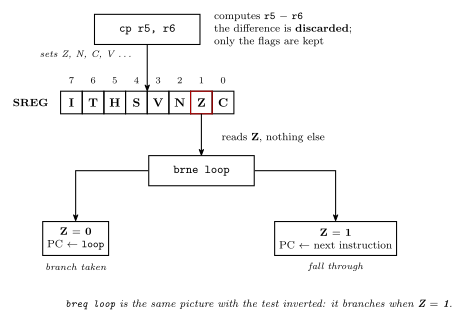
Figure 49: Compare-then-branch: the whole of an AVR conditional. cp performs the subtraction and throws the difference away, keeping only what it did to the flags; brne then reads exactly one of them and either loads the label’s address into the program counter or lets execution fall through to the next instruction. The flag names and their order are those of the AVR status register; the outline on Z marks the one flag brne tests.
Figure 49 is worth reading as the reason labels matter. The branch does not encode “go back three instructions” in a form you have to count out by hand; it names a label, and the assembler works out the address — the same service it performs for jmp RESET at the top of the file.
Two consequences for the template above. First, a loop that should sometimes end is still written as a label plus a branch, not as a special construct: the body falls through when the condition fails. Second, nothing may sit between the flag-setter and the branch that disturbs the flag being tested — the status register is a single shared piece of state, and the instruction in between will happily overwrite it.
The two branches above are the equality pair. The other eight — including the signed and unsigned less than pairs that a loop bound usually needs — and the loop idioms built from them are in avr-branches-and-jumps.
When the program calls procedures
The template above has no stack, because nothing in it calls anything. The moment a program uses call or rcall — or push — the stack pointer must be set first, and it goes at the top of RESET:, before any of the other initialisation:
RESET:
    ldi  r16, low(RAMEND)
    out  SPL, r16
    ldi  r16, high(RAMEND)
    out  SPH, r16
    ...                      ; then set DDRs and the rest as before
RAMEND is the last SRAM address, 0x08FF; the stack starts there and grows downward. Why it has to, and what call and ret do with it, is procedures-and-the-stack. A C program gets these four instructions for free from the compiler’s start-up code.
Variables and constants
The template holds only code. Variables and tables of constants go in the other segments (assembly-process), chosen by .dseg and .cseg:
.include "m324Adef.inc"
.def    temp = r16              ; a name for a register

        .dseg                   ; SRAM: space only
count:  .byte 1                 ; one byte, at 0x0100

        .cseg                   ; flash: code and constants
        jmp  RESET              ; vector table
RESET:
        ldi  temp, low(RAMEND)  ; stack pointer, if anything is called
        out  SPL, temp
        ldi  temp, high(RAMEND)
        out  SPH, temp
        ...                     ; initialisation
loop:
        ...                     ; main code
        jmp  loop

digits: .db  63, 6, 91, 79, 102, 109, 125, 7, 127, 111   ; seven-segment patterns, 0 to 9
Three rules come with it:
- A variable is a label on a
.bytein the data segment. It gets an address,0x0100for the first one, but no value. The program has to store something there, withsts count, tempfor example, before reading it. - Constants go in the code segment, out of the path of execution. The CPU runs whatever is in program memory at the PC, so a table in the middle of the code would be executed as if it were instructions. After the main loop’s
jmp loopis safe, because execution never gets there. Betweenjmp RESETandRESET:is safe for the same reason, but only in a program that uses no interrupts, because that is where the interrupt vectors go.digitsis ten bytes, an even number, so it fills five words with no pad (assembly-process). - A constant is read with
lpm, at its byte address, the label times 2, in Z (memory-models).
Why it ends in an infinite loop
loop: … jmp loop is not a placeholder. A microcontroller program has nowhere to return to — there is no operating system underneath it, and the CPU keeps fetching whatever comes next for as long as it has power. So the main body of an AVR program is a loop that never exits, and “do this repeatedly”, which is how nearly every lab task is worded, is the normal shape rather than a special case.
The division of labour that follows: anything that should happen once goes in the RESET handler (setting DDRs, loading constants), and anything that should happen forever goes in the loop (reading inputs, computing, writing outputs).
See also
- avr-branches-and-jumps — the full branch table, jumps, and the
if/loop idioms · procedures-and-the-stack —call,retand the stack - avr-interrupts — what goes in the vector table, and the handlers after it
- avr-instructions · avr-io-ports · avr-architecture
- assembly-process — statement fields, directives, segments and the two-pass assembler · instruction-set-architecture — assembly, the assembler and the toolchain
- memory-models — the program address space the vector table sits at the bottom of · memory-technologies — flash and SRAM, the memories behind
.csegand.dseg - week6-lab-avr-io-ports — Lab 10, where the template is first used
- 2026-10-08-assembly-process — Lecture 20: how the assembler turns the template into machine code
SPI on the AVR
The Serial Peripheral Interface, and the ATmega324A’s SPI port: the four signals, how two shift registers exchange a byte, one transfer in time, the ways to connect several slaves, the pins, the three registers, the clock rate, code to send and receive, the interrupt, and the USARTs as extra SPI masters. Where SPI sits among serial links, next to the UART and I²C, is in serial-communication. First met in 2026-10-05-more-io. The datasheet covers the SPI on pages 166 to 174.
What SPI is
SPI is a synchronous serial bus with one master and one or more slaves (serial-communication).
- Synchronous: the master sends a clock, and both ends move a bit on each pulse of it. Nothing about speed has to be agreed beforehand, except that the master must not go faster than the slave can follow.
- Full duplex: there is a data wire in each direction, and every clock pulse moves one bit each way.
- The master starts every transfer and makes the clock. A slave only answers.
| Signal | Driven by | Carries |
|---|---|---|
| SCK (also written SCLK) | master | serial clock, one pulse per bit |
| MOSI | master | Master Out, Slave In |
| MISO | slave | Master In, Slave Out |
| \(\overline{\text{SS}}\) | master | Slave Select, active low: a slave takes part only while its \(\overline{\text{SS}}\) is 0 |
The names say which end drives each wire, so the wiring is MOSI to MOSI and MISO to MISO. It is not crossed over the way a UART’s Tx and Rx are.
The exchange: two shift registers in a ring
Master and slave each have an 8-bit shift register (shift-registers). MOSI joins the master’s MSB end to the slave’s LSB end, and MISO joins the slave’s MSB end to the master’s LSB end. Together they are one 16-bit register bent into a ring, and each SCK pulse rotates it by one place. The hardware view, with the clock generator and the select pins, is drawn in 2026-10-05-more-io.
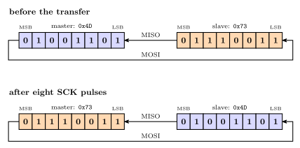
Figure 50: The exchange as data. Before the transfer the master’s register holds 0x4D, shaded blue, and the slave’s holds 0x73, shaded orange. Each SCK pulse moves every bit one place round the ring: towards the MSB inside each register, and across on MOSI or MISO at the ends. After eight pulses each byte has gone all the way across and the shading has changed sides: the master holds 0x73 and the slave 0x4D. A byte has been sent in each direction at once.
Two consequences follow from the ring:
- To receive, the master must send. There is no read-only transfer. To collect a byte from a slave, the master sends a dummy byte, often
0x00or0xFF, and keeps what comes back. - To send is also to receive. Every byte sent brings one back. If it is of no interest, the master reads it and throws it away.
Worked: one exchange, clock by clock
The master’s register holds 0x4D (0100 1101) and the slave’s holds 0x73 (0111 0011), and the bytes go most significant bit first. Each clock, each register’s top bit leaves on its data wire, the other seven move up one place, and the bit arriving from the other end fills the bottom:
| After clock | MOSI carried | MISO carried | Master | Slave |
|---|---|---|---|---|
| start | 0100 1101 |
0111 0011 |
||
| 1 | 0 | 0 | 1001 1010 |
1110 0110 |
| 2 | 1 | 1 | 0011 0101 |
1100 1101 |
| 3 | 0 | 1 | 0110 1011 |
1001 1010 |
| 4 | 0 | 1 | 1101 0111 |
0011 0100 |
| 5 | 1 | 0 | 1010 1110 |
0110 1001 |
| 6 | 1 | 0 | 0101 1100 |
1101 0011 |
| 7 | 0 | 1 | 1011 1001 |
1010 0110 |
| 8 | 1 | 1 | 0111 0011 |
0100 1101 |
The MOSI column, read down, is 0100 1101, the master’s byte, and the MISO column is 0111 0011, the slave’s. After 8 clocks the master holds 0x73 and the slave 0x4D.
One transfer in time
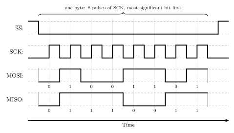
Figure 51: One SPI transfer in the AVR’s default mode: SCK idles low, both ends sample their incoming data wire on each rising edge of SCK (the dotted lines), and both put out their next bit on each falling edge. The master pulls \(\overline{\text{SS}}\) low to select the slave, and the slave’s first bit appears on MISO at that moment. Eight clock pulses then carry 0x4D from master to slave on MOSI and 0x73 from slave to master on MISO, most significant bit first, with the bit values written under each data wire. Raising \(\overline{\text{SS}}\) ends the transfer. The data wires matter only while \(\overline{\text{SS}}\) is low, so they are drawn only then.
A transfer, from the master’s side:
- Pull \(\overline{\text{SS}}\) low. The selected slave wakes up and puts its first bit on MISO.
- Write the byte to the data register. The SPI hardware makes eight pulses on SCK. On each rising edge both ends read the data wire coming in; on each falling edge both shift their next bit out.
- Wait for the transfer-complete flag, then read the byte that came in.
- Send more bytes the same way, or raise \(\overline{\text{SS}}\) to end the transfer.
The AVR’s SPI hardware never moves \(\overline{\text{SS}}\) itself in master mode. Steps 1 and 4 are the program’s job, done with PORTB.
Clock polarity and phase
The figure shows the AVR’s mode after reset. Two bits in the control register change it: CPOL, which level SCK rests at, and CPHA, whether data is read on the first or the second edge of each pulse. Together they number four modes:
| Mode | CPOL | CPHA | SCK when idle | Data read on |
|---|---|---|---|---|
| 0 | 0 | 0 | low | the rising edge, the first of each pulse |
| 1 | 0 | 1 | low | the falling edge, the second of each pulse |
| 2 | 1 | 0 | high | the falling edge, the first of each pulse |
| 3 | 1 | 1 | high | the rising edge, the second of each pulse |
A third setting is the bit order, MSB first or LSB first. A device’s datasheet says which mode and bit order it uses, and the master has to match it. As with a UART’s settings (serial-communication), nothing on the wires says which is in use, and a mismatch gives wrong bytes, not an error.
Several slaves
Both wirings are drawn in 2026-10-05-more-io.
Independent selects. SCK and MOSI go to every slave, and every slave’s MISO joins the one wire back to the master. Each slave has its own select line from the master, and the master pulls one low at a time. A slave whose \(\overline{\text{SS}}\) is high ignores SCK and lets go of MISO (the AVR as a slave makes all its SPI pins inputs), so only the selected slave drives the shared wire. Every slave costs one more master pin.
Daisy chain. One select line goes to all the slaves, and the data passes through them in turn: master MOSI into slave 1’s MOSI, each slave’s MISO into the next one’s MOSI, the last slave’s MISO back to the master’s MISO. The master’s register and the slaves’ registers make one ring, \(8 \times (\text{slaves} + 1)\) bits round. A chainable device acts on the byte it holds when \(\overline{\text{SS}}\) goes back high, so everything has to be in place by then.
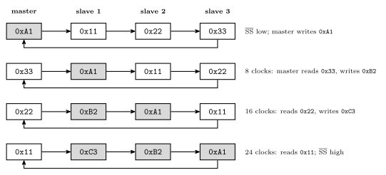
Figure 52: A daisy chain of three slaves as one long shift register, 32 bits round. Each row is the chain at one moment, read left to right in the direction the data moves, and the arrow underneath is the last slave’s MISO returning to the master. Shaded bytes are the ones the master has sent. Every 8 clocks move every byte one place along, so the first byte sent, 0xA1, ends up in the farthest slave, and the master receives the slaves’ old bytes, the farthest slave’s first. Between bytes the master reads what has arrived and writes the next byte to send.
Worked: which byte goes first?
To leave 0xA1 in slave 3, 0xB2 in slave 2 and 0xC3 in slave 1, send 0xA1, 0xB2, 0xC3, in that order, with \(\overline{\text{SS}}\) low for all 24 clocks. The byte for the farthest slave goes first, because every later byte pushes it one place further along. The three bytes that come back are the slaves’ previous contents, slave 3’s first.
The pins
The SPI port uses the upper half of port B (avr-io-ports):
| Port pin | Package pin | Signal | As master | As slave |
|---|---|---|---|---|
| PB4 | 5 | \(\overline{\text{SS}}\) | the program’s to use: make it an output | input |
| PB5 | 6 | MOSI | output: the program sets its DDRB bit |
input |
| PB6 | 7 | MISO | input | output: the program sets its DDRB bit |
| PB7 | 8 | SCK | output: the program sets its DDRB bit |
input |
Switching the SPI on forces some pins’ directions and leaves others to DDRB. A pin marked input is made an input by the hardware. A pin that has to be an output, the program has to make an output itself.
The \(\overline{\text{SS}}\) pin in master mode. If PB4 is left as an input and something pulls it low, the AVR takes it that another master is selecting it as a slave. It clears MSTR0, becoming a slave, and sets the transfer-complete flag. A master therefore makes PB4 an output, usually as the select line for its slave, or else guarantees that it stays high. As an output it is an ordinary port pin and the SPI ignores it.
These same pins are the ones a programmer uses to download a program into the AVR, which is worth remembering when a device is attached to them.
The registers
| Register | Holds |
|---|---|
SPCR0 |
control: on/off, master or slave, bit order, clock mode, clock rate, interrupt enable |
SPSR0 |
status: the transfer-complete and write-collision flags, and the double-speed bit |
SPDR0 |
data: write a byte to send it, read the byte received |
The datasheet’s SPI chapter (pages 172 and 173) calls these SPCR, SPSR and SPDR, and its bit names have no 0 either. In C and assembly every name carries the 0: SPCR0, SPE0, MSTR0, SPIF0, and SPR1 becomes SPR10. The I/O register summary still names the registers SPCR and SPSR, but writes the bit names with the 0, except that it labels bit 1 SPR01 where the header has SPR10.
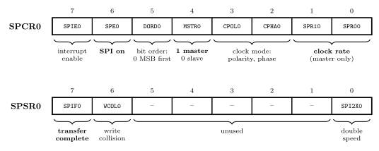
Figure 53: The SPI port’s two control and status registers, with the names used in code. SPCR0 sets the port up: bit 6 turns it on, bit 4 chooses master or slave, bit 5 the bit order, bits 3 and 2 the clock mode, and the bottom two bits the clock rate when it is a master. Bit 7 lets the end of a transfer raise an interrupt. In SPSR0, bit 7 is the flag that says a transfer has finished, bit 6 reports a write to the data register in the middle of a transfer, and bit 0 doubles the master’s clock rate, a third clock-rate bit to go with the two in SPCR0. Every bit is 0 after reset, so the port starts switched off.
SPCR0: the set-up
| Bit | Name | When 1 | When 0 |
|---|---|---|---|
| 7 | SPIE0 |
the end of a transfer raises an interrupt | no interrupt |
| 6 | SPE0 |
the SPI port is on | off: the pins belong to port B |
| 5 | DORD0 |
LSB first | MSB first |
| 4 | MSTR0 |
master | slave |
| 3 | CPOL0 |
SCK idles high | SCK idles low |
| 2 | CPHA0 |
data read on the second edge of each pulse | data read on the first edge |
| 1:0 | SPR10, SPR00 |
the clock rate, with SPI2X0 (below) |
SPSR0: what has happened
| Bit | Name | Set when | Cleared by |
|---|---|---|---|
| 7 | SPIF0 |
a transfer has finished; also when a master’s \(\overline{\text{SS}}\) input is pulled low | the interrupt handler running, or reading SPSR0 and then SPDR0 |
| 6 | WCOL0 |
SPDR0 was written while a transfer was going on |
reading SPSR0 and then SPDR0 |
| 0 | SPI2X0 |
(a setting) 1 doubles the master’s SCK |
Bits 5 to 1 are unused.
SPDR0: the data
Writing SPDR0 starts a transfer when the port is a master: the byte goes into the shift register and the eight clock pulses begin. Reading SPDR0 gives the byte received. The two directions are buffered differently. On the way out there is only the shift register, so a byte written during a transfer is not sent and sets WCOL0 instead. On the way in the finished byte is copied to a buffer, where it waits until the next byte is complete, so it has to be read before then or it is lost.
Choosing the clock rate
In master mode three bits pick the divider:
SPI2X0 |
SPR10 |
SPR00 |
SCK | At 8 MHz |
|---|---|---|---|---|
| 0 | 0 | 0 | \(f_{OSC}/4\) | 2 MHz |
| 0 | 0 | 1 | \(f_{OSC}/16\) | 500 kHz |
| 0 | 1 | 0 | \(f_{OSC}/64\) | 125 kHz |
| 0 | 1 | 1 | \(f_{OSC}/128\) | 62.5 kHz |
| 1 | 0 | 0 | \(f_{OSC}/2\) | 4 MHz |
| 1 | 0 | 1 | \(f_{OSC}/8\) | 1 MHz |
| 1 | 1 | 0 | \(f_{OSC}/32\) | 250 kHz |
| 1 | 1 | 1 | \(f_{OSC}/64\) | 125 kHz |
SPI2X0 halves the divider chosen by the other two. Eight codes give seven dividers, because 64 appears twice. After reset all three bits are 0, which is divider 4.
In slave mode these bits do nothing, because the slave’s clock comes from the master. A slave samples the incoming SCK with its own clock and is only guaranteed to keep up to \(f_{OSC}/4\), 2 MHz at 8 MHz.
A byte takes 8 SCK periods, which is \(8 \times\) divider CPU cycles: 16 cycles (2 µs) at the fastest, 1024 (128 µs) at the slowest.
Worked: the slowest master clock
Which bits must be 1 to switch the SPI on as a master with the slowest clock, and what is written to SPCR0?
The slowest divider is 128, code SPI2X0 SPR10 SPR00 = 0 1 1. Add SPE0 to switch the port on and MSTR0 to make it a master. Nothing in SPSR0 needs to be 1, since SPI2X0 must stay 0.
SPCR0 = (1<<SPE0) | (1<<MSTR0) | (1<<SPR10) | (1<<SPR00); /* 0101 0011 = 0x53 */Bits 6, 4, 1 and 0 make 0100 0000 + 0001 0000 + 0000 0010 + 0000 0001 = 0x53, and SCK is \(8\text{ MHz}/128 = 62.5\) kHz.
Worked: a 1 MHz clock
\(8\text{ MHz}/1\text{ MHz} = 8\), which is code 1 0 1: SPR00 in SPCR0 and SPI2X0 in SPSR0.
SPCR0 = (1<<SPE0) | (1<<MSTR0) | (1<<SPR00);
SPSR0 = (1<<SPI2X0);
Sending and receiving, by polling
A master that sends and receives one byte at a time:
#include <avr/io.h>

#define SS_PIN 4                          /* PB4 used as the slave's select */

void spi_init_master(void) {
    DDRB  |= (1<<SS_PIN) | (1<<5) | (1<<7);   /* SS, MOSI, SCK outputs; MISO stays an input */
    PORTB |= (1<<SS_PIN);                     /* SS high: no slave selected yet             */
    SPCR0  = (1<<SPE0) | (1<<MSTR0) | (1<<SPR00);   /* on, master, f/16 = 500 kHz        */
}

uint8_t spi_exchange(uint8_t out) {
    SPDR0 = out;                          /* writing starts the eight clocks   */
    while (!(SPSR0 & (1<<SPIF0))) {       /* wait for the transfer to finish   */
    }
    return SPDR0;                         /* the byte that came back; reading  */
                                          /* SPSR0 then SPDR0 clears SPIF0     */
}
and a transfer of two bytes, the second one to collect the slave’s reply:
uint8_t reply;

PORTB &= ~(1<<SS_PIN);                    /* select the slave                */
spi_exchange(0x4D);                       /* send; what comes back is ignored */
reply = spi_exchange(0x00);               /* send a dummy byte to read one   */
PORTB |= (1<<SS_PIN);                     /* deselect                        */
The rules it follows:
- The program moves \(\overline{\text{SS}}\), low before the first byte and high after the last.
- One byte at a time. Write
SPDR0, wait forSPIF0, then write the next. A write during a transfer is lost. - To read, send.
At 500 kHz the wait is 16 µs, 128 CPU cycles, against about a millisecond for a UART frame at 9600 baud. Waiting by polling (polling-and-interrupts) is often the sensible choice for SPI.
As a slave, the AVR only makes MISO an output and switches the port on with MSTR0 left at 0:
void spi_init_slave(void) {
    DDRB |= (1<<6);                       /* MISO is the slave's one output */
    SPCR0 = (1<<SPE0);                    /* on, slave                      */
}
A slave can never start anything. It puts the reply it wants to give in SPDR0 ahead of time, and when the master has clocked a byte through, SPIF0 is set and SPDR0 holds what the master sent.
The interrupt
| Event | Flag (SPSR0) |
Enable (SPCR0) |
Handler |
|---|---|---|---|
| transfer complete | SPIF0 |
SPIE0 |
ISR(SPI_STC_vect) |
It is vector 20 in the table (avr-interrupts), and running the handler clears SPIF0. The usual use is a queue of bytes: the handler reads the byte that has just arrived and writes the next one to SPDR0, so a run of bytes goes out without the main program waiting on each. On a slave, the interrupt is how the program finds out that the master has just exchanged a byte with it.
The USARTs as SPI masters
Each USART can also work as an SPI master, by setting its mode bits UMSELn1:0 in UCSRnC to 11 (avr-usart). Its pins then take the SPI roles:
| USART | SCK | Data out (MOSI) | Data in (MISO) |
|---|---|---|---|
| USART0 | XCK0, PB0 | TXD0, PD1 | RXD0, PD0 |
| USART1 | XCK1, PD4 | TXD1, PD3 | RXD1, PD2 |
There is no select pin: the program drives any spare port pin as \(\overline{\text{SS}}\). A USART in this mode can only be a master. With the SPI port as well, the ATmega324A can be the master on three separate SPI buses.
Common mistakes
- Crossing MOSI and MISO as if they were a UART’s Tx and Rx. MOSI goes to MOSI.
- Expecting to read without sending. The master gets a byte only by sending one.
- Leaving PB4 an input in master mode. If it floats or is pulled low,
MSTR0is cleared and the AVR silently becomes a slave. - Not setting
DDRBfor MOSI and SCK on a master, or MISO on a slave. Switching the SPI on does not make those pins outputs. - Waiting for the hardware to drive \(\overline{\text{SS}}\). A master has to do it in software.
- Writing
SPDR0before the last transfer has finished. The byte is not sent andWCOL0is set. - Using the datasheet names
SPCR,SPE,SPR1in code. The header names have a0:SPCR0,SPE0,SPR10. - Mismatched mode or bit order with the slave device: wrong bytes and no error.
- Clocking an AVR slave faster than \(f_{OSC}/4\).
- Loading a daisy chain nearest slave first. The first byte sent ends up in the farthest slave.
See also
- serial-communication — SPI next to the UART and I²C, bus masters and slaves, bit bashing
- shift-registers — the register at each end of the ring
- avr-io-ports — port B,
DDRB, and the pins’ alternate functions - avr-usart — the USART, and its mode bits for master SPI
- avr-interrupts · polling-and-interrupts — the
SPI_STCinterrupt, or waiting onSPIF0 - bit-masking · c-preprocessor-and-avr-headers —
(1<<SPE0)and where the names come from - week10-lab-adc-and-spi — Lab 16, the SPI port driving an LED matrix
- 2026-10-05-more-io — Lecture 19
AVR Timers and Counters
The ATmega324A’s three timer/counter units: what they are, which pins and registers belong to each, how their clock is chosen and prescaled, the modes that decide what the count does when it reaches its top, the output compare actions that let a match drive a pin, and the one formula that turns a wanted event frequency into register values. From 2026-09-14-flow-of-control and 2026-09-17-pulse-width-modulation, with the register-level detail from week8-lab-avr-timers. PWM, the timers’ main use, has its own note: pulse-width-modulation.
Timer, counter
- A counter is a binary up/down counter clocked on some event.
- A timer is a counter clocked by a regular clock.
One piece of hardware, two names for what its clock is. Clock it from an external pin and each count is an event; clock it from the system clock and each count is a fixed slice of time, so the count is elapsed time. It is the wide, fast, silicon version of the counters of counters, and it is separate hardware from the CPU: once configured it counts, compares and drives its pins with no instructions running, which is the whole reason to have it.
Three things a timer/counter is used for, in this course:
| Use | Clock | The event |
|---|---|---|
| Timing — do something every 100 ms, toggle an LED, tick a clock | system clock ÷ prescaler | the count reaching a compare value or wrapping, at a known interval |
| Counting — how many pulses arrived on a pin | edges on the external pin Tn |
the count reaching a compare value: that many pulses |
| PWM — an adjustable-width pulse on a pin, in hardware | system clock ÷ prescaler | the compare match switching the OCnx pin partway through each sweep |
The three units
| Timer/Counter 0 | Timer/Counter 1 | Timer/Counter 2 | |
|---|---|---|---|
| Width | 8-bit (0–255) | 16-bit (0–65535) | 8-bit (0–255) |
| Output compare pins | PB3 = OC0A, PB4 = OC0B |
PD5 = OC1A, PD4 = OC1B |
PD7 = OC2A, PD6 = OC2B |
| External clock pin | PB0 = T0 |
PB1 = T1 |
none — TOSC1/TOSC2 (PC6/PC7) take a separate crystal instead |
| Prescaler taps | 1, 8, 64, 256, 1024 | 1, 8, 64, 256, 1024 | 1, 8, 32, 64, 128, 256, 1024 |
| Modes | Normal, CTC, Fast PWM, Phase Correct PWM | Normal, CTC, Fast PWM, PC PWM, PFC PWM | Normal, CTC, Fast PWM, Phase Correct PWM |
| Count register | TCNT0 |
TCNT1H:TCNT1L |
TCNT2 |
| Control registers | TCCR0A, TCCR0B |
TCCR1A, TCCR1B, TCCR1C |
TCCR2A, TCCR2B |
| Compare registers | OCR0A, OCR0B |
OCR1AH:OCR1AL, OCR1BH:OCR1BL |
OCR2A, OCR2B |
| Interrupt registers | TIMSK0, TIFR0 |
TIMSK1, TIFR1 |
TIMSK2, TIFR2 |
Every unit has two compare units, A and B, each with its own register and its own pin. Timer 1 is the one to reach for when 255 is not enough: its 16 bits give periods 256 times longer at the same prescaler, and it is the timer Lab 12 sets up. Timer 2 is the one with a separate clock source, for real-time-clock use. The T/C 3 in the family datasheet’s block diagram is on the ATmega1284, not this chip (avr-architecture).
The pins are shared with GPIO. OC0A is PB3 until timer 0 is told to drive it; configuring a compare output takes the pin away from PORTB and hands it to the timer. The DDR bit must still be set to output, since the timer only decides what the pin shows, not whether it drives.
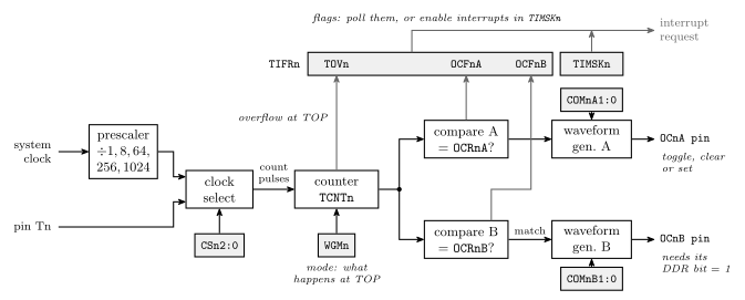
Figure 54: One timer/counter unit, from clock to pins. The clock select multiplexer feeds the counter either a prescaler tap or an edge on the external pin, or nothing; the counter increments on each pulse of whatever it is given. Two compare registers are each checked against the count every tick, and a match raises that unit’s flag and fires the waveform generator for its pin. Reaching the top of the count raises the overflow flag and, depending on the mode, wraps the count. The flags collect in TIFRn, where a program can poll them or, with the matching bits set in TIMSKn, have them raise an interrupt. Every box is configured through I/O registers and then runs with no CPU involvement.
Registers: data, control, interrupt
A timer is configured the way a port is — through I/O registers (avr-io-ports) — and its registers sort into the same three kinds:
| Timer registers | Port equivalent | ||
|---|---|---|---|
| data | TCNTn — the current count |
PIN / PORT |
read it to see where the count is; write it to preset |
| control | TCCRnA, TCCRnB (TCCR1C) — mode, clock, pin action; OCRnA, OCRnB — the values to match |
DDR |
set once, then leave |
| interrupt | TIMSKn — which events raise an interrupt; TIFRn — which events have happened |
— | read the flags by polling, or enable interrupts: avr-interrupts |
Where they are
The timer registers are spread across both the in/out range and the extended I/O space that only lds/sts reach (avr-io-ports):
| Register | I/O address | Data-memory address |
|---|---|---|
TCNT0 |
0x26 |
0x46 |
TCNT1L / TCNT1H |
— | 0x84 / 0x85 |
TCNT2 |
— | 0xB2 |
In C none of this matters: avr/io.h defines every one of them as a memory-mapped byte (c-preprocessor-and-avr-headers), and TCNT0, OCR1A and TCCR2B are assigned to like variables.
16-bit registers
Timer 1’s count and compare registers are two bytes each, and the hardware guards them with a shared temporary register so that a 16-bit value is read or written atomically: write the high byte first, then the low; read the low byte first, then the high. In assembly:
    ldi  r16, high(4321)
    sts  OCR1BH, r16       ; high byte first — goes into the temp register
    ldi  r16, low(4321)
    sts  OCR1BL, r16       ; low byte — both bytes land together
In C the compiler knows the rule, and OCR1B = 4321; is the whole thing. The H/L names still exist, but OCR1A, OCR1B, TCNT1 and ICR1 are 16-bit variables in the header.
The read rule has a consequence: reading TCNT1H on its own gives a stale value. Reading the low byte is what copies the high byte into the temporary register, and a read of the high byte returns that copy. So for the top half of the count, read the whole of TCNT1 and shift, as in TCNT1 >> 8, which reads the low byte first (below).
Choosing the clock
The count advances once per rising edge of whatever the clock select field CSn2:0 in TCCRnB picks — drawn as a multiplexer in 2026-09-14-flow-of-control:
CSn2 |
CSn1 |
CSn0 |
Timers 0 and 1 | Timer 2 |
|---|---|---|---|---|
| 0 | 0 | 0 | no clock — timer stopped | no clock |
| 0 | 0 | 1 | clk / 1 (no prescaling) | clk / 1 |
| 0 | 1 | 0 | clk / 8 | clk / 8 |
| 0 | 1 | 1 | clk / 64 | clk / 32 |
| 1 | 0 | 0 | clk / 256 | clk / 64 |
| 1 | 0 | 1 | clk / 1024 | clk / 128 |
| 1 | 1 | 0 | external pin Tn, falling edge |
clk / 256 |
| 1 | 1 | 1 | external pin Tn, rising edge |
clk / 1024 |
Two things to read off the table. A timer with CS = 000 does not run, which is both the reset state and the way to stop one. And timer 2’s codes are different — it spends the two external-pin codes on its extra prescaler taps — so a CS value copied from a timer-1 example means something else on timer 2.
The prescaler is a chain of dividers on the system clock (8 MHz on the lab boards), and each tap makes every count last that many system cycles. With an 8-bit timer the full 0-to-255 sweep therefore takes \(256 \cdot N\) cycles:
| Prescaler \(N\) | Tick | Sweep of 256 counts (8 MHz) | Sweep of 65536 counts (timer 1) |
|---|---|---|---|
| 1 | 0.125 µs | 32 µs | 8.2 ms |
| 8 | 1 µs | 256 µs | 65.5 ms |
| 64 | 8 µs | 2.05 ms | 524 ms |
| 256 | 32 µs | 8.19 ms | 2.1 s |
| 1024 | 128 µs | 32.8 ms | 8.4 s |
Coarse control over the period comes from this table; fine control comes from the compare registers and the mode.
Worked: a slow count from TCNT1 >> 8
With the clock divided by 1024, how quickly does TCNT1 >> 8 go up?
Timer 1 then counts \(8\ \text{MHz} / 1024 = 7812.5\) times a second. Shifting right by 8 drops the bottom eight bits, so what is left goes up by one every \(2^8 = 256\) counts:
\[\frac{7812.5}{256} = 30.5\ \text{Hz}, \quad\text{once every } 32.8\ \text{ms}.\]
TCNT1 >> 8 is the high byte of the count. It runs from 0 to 255 and comes back round to 0 every \(65\,536 / 7812.5 = 8.4\) seconds.
The same reasoning works for any shift. Each bit of a counter changes half as often as the bit below it, so TCNT1 >> k goes up \(7812.5 / 2^k\) times a second: 3906 for a shift of 1, 1953 for 2, and so on down to 30.5 for 8. A single bit is a square wave: (TCNT1 >> 12) & 1 changes every \(2^{12} = 4096\) counts, 0.52 s, which is enough to blink something about once a second without a single interrupt.
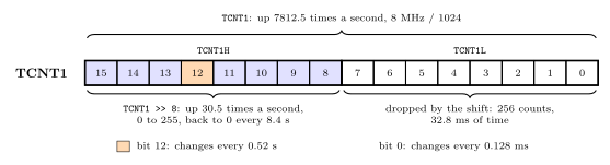
Figure 55: Timer 1’s count as a set of slower counters. With the clock divided by 1024 the whole of TCNT1 goes up 7812.5 times a second. Each bit changes half as often as the one to its right, so bit 8 changes once every 256 counts, and the top byte, TCNT1 >> 8, is a counter of its own that goes up 30.5 times a second and wraps every 8.4 s. Bit 12, shaded, changes every 0.52 s on its own.
In code, the timer only needs its prescaler, and it runs freely in normal mode:
TCCR1A = 0;
TCCR1B = (1<<CS12) | (1<<CS10);              /* normal mode, clock / 1024 */

uint8_t start = TCNT1 >> 8;
while ((uint8_t)((TCNT1 >> 8) - start) < 61) { }   /* 61 x 32.8 ms = 2.0 s */
The subtraction is done in 8 bits on purpose. When the count wraps from 255 to 0, now - start still comes out as the number of steps in between, so long as fewer than 256 have passed. week10-lab-adc-and-spi paces all its programs this way.
Modes: what happens at TOP
The waveform generation mode bits — WGM02:0 for the 8-bit timers, WGM13:0 for timer 1, split across TCCRnA and TCCRnB — decide what the count does when it reaches its TOP, and what TOP is:
| Mode | TOP | At TOP | Timer 0 WGM02:0 |
Timer 1 WGM13:0 |
|---|---|---|---|---|
| Normal | 0xFF / 0xFFFF | wrap to 0, set TOVn |
000 (0) |
0000 (0) |
| CTC — clear timer on compare match | OCRnA |
clear to 0, set OCFnA |
010 (2) |
0100 (4) |
| Fast PWM, fixed top | 0xFF | wrap to 0 | 011 (3) |
0101–0111 (8-, 9-, 10-bit) |
| Fast PWM, top in a register | OCRnA |
wrap to 0 | 111 (7) |
1111 (15; 1110 uses ICR1) |
| Phase correct PWM | 0xFF or OCRnA |
count back down | 001 (1), 101 (5) |
0001–0011, 1011 |
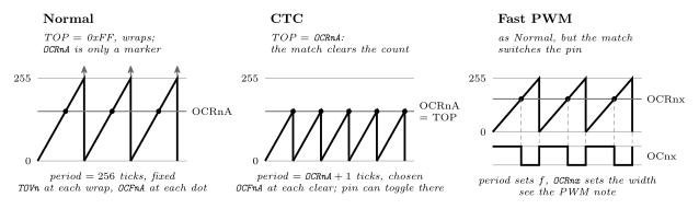
Figure 56: The three modes this course uses, as the count against time. In normal mode the counter runs to its full range and wraps; a compare value is just a marker it passes on the way, and the period is fixed at \(2^{8}\) or \(2^{16}\) ticks. In CTC mode reaching OCRnA clears the counter, so the compare value is the period and can be set to anything — the mode for producing an event at a chosen rate. In fast PWM the counter runs as in normal mode (or, in the register-top variant, as in CTC) while the compare match switches a pin partway through each sweep: the period sets the frequency and the compare value sets the pulse width. The same counter and the same compare registers produce all three; the mode bits only change what the top of the count means.
Normal is the mode after reset and the mode for a free-running count: read TCNTn to see how much time has passed, or let it overflow and take the overflow as the tick. CTC is the mode for an event every \(X\) ticks: the period is OCRnA + 1 exactly, with no wasted counts, and the count never exceeds the compare value. Both PWM modes are in pulse-width-modulation.
Output compare: what a match does to the pin
Each compare unit has two compare output mode bits, COMnx1:0 in TCCRnA, that decide what happens to the OCnx pin when TCNTn equals OCRnx. In the non-PWM modes (Normal, CTC):
COMnx1 |
COMnx0 |
On compare match |
|---|---|---|
| 0 | 0 | normal port operation — the pin belongs to the port, timer disconnected |
| 0 | 1 | toggle OCnx |
| 1 | 0 | clear OCnx — set the output low |
| 1 | 1 | set OCnx — set the output high |
Toggle is the useful one for a square wave: a CTC count that toggles the pin on every match produces a waveform whose frequency is half the match frequency, since it takes two matches for one full cycle. In the PWM modes the same bits select non-inverting (10) or inverting (11) output, and 01 becomes toggle OCnA on match only in the register-top mode — see pulse-width-modulation.
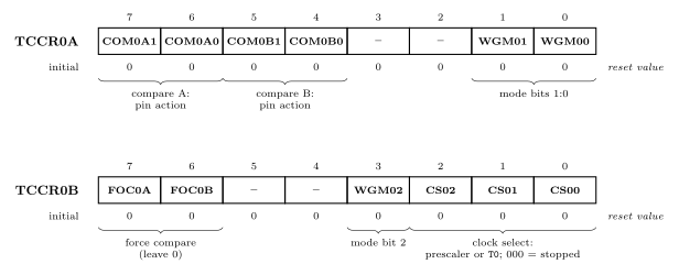
Figure 57: The two control registers of timer/counter 0, bit by bit, in the datasheet’s three-row form. The compare output mode fields sit at the top of TCCR0A, one two-bit field per compare unit; the three waveform generation mode bits are split, two at the bottom of TCCR0A and one in the middle of TCCR0B; the clock select field is the bottom three bits of TCCR0B. The two force-output-compare bits are for tests and are left alone. Every bit resets to 0, which decodes as normal mode, pins disconnected, timer stopped — so a timer does nothing until a program writes both registers. Timer 2’s registers have the same layout; timer 1 spreads the same fields over three registers with a fourth WGM bit.
Setting them from C uses the bit names from the header as shift counts, the idiom of bit-masking: TCCR1B = (1<<WGM12) | (1<<CS11) | (1<<CS10); selects CTC mode with clock ÷ 64 on timer 1, and TCCR0A = (1<<COM0A0); makes OC0A toggle on match. Write the whole register rather than |= when setting a timer up, so that nothing left over from before survives.
The master formula
Every timing question reduces to one relation between the clock, the prescaler and the top of the count:
\[f_{event} = \frac{f_{clk\_I/O}}{N \cdot (TOP + 1)}\]
- \(f_{clk\_I/O}\) is the device clock — 8 MHz on the ATmega324A boards.
- \(N\) is the prescaler: 1, 8, 64, 256 or 1024.
- \(TOP\) is the highest value the count reaches before it restarts: 255 or 65535 in normal mode and the fixed PWM modes, the value in
OCRnAin CTC mode and the register-top PWM modes. The \(+1\) is because the count from 0 to \(TOP\) takes \(TOP + 1\) ticks. - \(f_{event}\) is how often the count restarts — which is how often whatever is tied to the restart happens.
What the event is depends on what is hung off the timer:
| Tied to the restart | \(f_{event}\) is | Note |
|---|---|---|
| a pin set to toggle on match | the toggle rate | the resulting square wave has frequency \(f_{event}/2\) — one cycle needs a rise and a fall |
| a PWM output | the pulse rate | one falling edge per period in non-inverting mode, one rising edge in inverting |
| an interrupt | how often the handler runs | avr-interrupts |
Worked example. Toggle a pin 8 times a second (a 4 Hz square wave) from timer 1: \(f_{event} = 8\), so \(N \cdot (TOP + 1) = 8\,000\,000 / 8 = 1\,000\,000\):
| \(N\) | \(TOP + 1\) | \(TOP\) | Usable? |
|---|---|---|---|
| 1 | 1 000 000 | 999 999 | no — exceeds 65535 |
| 8 | 125 000 | 124 999 | no — exceeds 65535 |
| 64 | 15 625 | 15 624 | yes — integer and fits |
| 256 | 3 906.25 | — | no — not an integer |
| 1024 | 976.5625 | — | no — not an integer |
So OCR1A = 15624 in CTC mode with CS12:0 = 011. The recipe is always the same: fix \(f_{event}\), try each \(N\), keep the one that gives an integer \(TOP\) that fits the timer’s width; if none does exactly, take the nearest and accept the error. Lab 12 works this example in full (week8-lab-avr-timers).
Reading the flags
A program finds out that a match or overflow happened either by polling TIFRn, below, or by enabling the matching bit in TIMSKn so that the event raises an interrupt (avr-interrupts). When an interrupt is taken, the hardware clears the flag itself; a polling program must clear it. Two things about those flags are unlike anything on a port:
- A flag is cleared by writing a 1 to it, not a 0:
TIFR1 = (1<<OCF1A);clears the compare-A flag and leaves the others alone (writing 0 to a bit does nothing). It is the one place where|=is a mistake, since it would clear every flag that happened to be set. - The flag is set by the hardware whether or not the pin is connected or an interrupt is enabled, so a CTC timer with
COM = 00still raisesOCFnAevery period — a free periodic tick for a program that just needs to wait.
/* wait one period of a running CTC timer 1 */
while (!(TIFR1 & (1<<OCF1A))) { }   /* spin until the flag is set */
TIFR1 = (1<<OCF1A);                  /* clear it for next time */
See also
- pulse-width-modulation — the PWM modes, duty cycle and their formulas
- week8-lab-avr-timers — Lab 12:
TCCR1A/B/Cbit by bit, the master formula worked, two programs - week9-lab-avr-pwm — Lab 13: PWM on timers 0 and 1 · week9-lab-avr-interrupts — Lab 14: a 10 ms tick from timer 1
- week10-lab-adc-and-spi — Lab 16: a free-running timer 1 read as
TCNT1 >> 8to pace four programs - software-timers — one timer serving every timing job in a program
- avr-io-ports — I/O registers, the two address spaces,
in/outversuslds/sts - c-preprocessor-and-avr-headers — why
TCCR0AandOCR1Bcan be assigned to · bit-masking —(1<<CS11) - counters — the digital-logic counter this is built from · avr-architecture — the block diagram
- 2026-09-14-flow-of-control — Lecture 15 · 2026-09-17-pulse-width-modulation — Lecture 16
The AVR USART
The ATmega324A’s serial port: the pins, the five registers a program uses, how to set the baud rate, how to send and receive a byte, and the three interrupts. What a UART frame is, and what baud rate and parity mean, are in serial-communication. First met in 2026-09-24-serial-io. The datasheet covers the USART on pages 175 to 201.
What it is
A USART is a Universal Synchronous and Asynchronous Receiver/Transmitter. The course uses it in its asynchronous mode, as a UART: frames with start and stop bits, no clock wire.
The ATmega324A has two, USART0 and USART1. USART0’s pins are on port D:
| Pin | Name | Direction |
|---|---|---|
| PD0 | RXD0 |
receive: data coming in |
| PD1 | TXD0 |
transmit: data going out |
Turning the receiver or transmitter on takes its pin away from the port, in the same way a timer takes over its output-compare pin (avr-timers-and-counters).
The registers
| Register | Holds |
|---|---|
UDR0 |
the data: write a byte to send it, read to collect a received byte |
UCSR0A |
status flags, and two mode bits |
UCSR0B |
interrupt enables, receiver and transmitter enables |
UCSR0C |
the frame format |
UBRR0 (UBRR0H, UBRR0L) |
the baud rate |
The 0 in each name is the USART number. The datasheet writes the names with an n in its place, as in UDRn.
The data register
UDR0 is two registers at one address. A write goes to the transmit buffer. A read comes from the receive buffer. So
UDR0 = 'A';        /* send the letter A            */
c = UDR0;          /* collect whatever has arrived */
and reading UDR0 never returns the value that was written to it.
Behind each buffer is a shift register (shift-registers). A byte written to UDR0 waits there until the transmit shift register is free, is copied across, and is shifted out of TXD0 bit by bit, with the start bit, any parity bit and the stop bits added. On the way in, bits from RXD0 are shifted into the receive shift register, and the finished byte is copied to the receive buffer.
That makes the transmitter two bytes deep: one byte going out and one waiting behind it. It is why there are two separate “finished” conditions, below.
Control and status registers
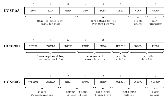
Figure 58: The three control and status registers of USART0, with their bits grouped by what they do. The top three bits of UCSR0A are the flags for the three serial events, and the top three bits of UCSR0B, directly beneath, are the interrupt enables for the same three events in the same order. UCSR0B also switches the receiver and transmitter on. UCSR0C sets the frame format. The number of data bits is the one setting split across two registers: UCSZ02 is in UCSR0B and UCSZ01:00 are in UCSR0C.
UCSR0A: what has happened
| Bit | Name | Set when | Cleared by |
|---|---|---|---|
| 7 | RXC0 |
receive complete: a byte has arrived and has not been read | reading UDR0 |
| 6 | TXC0 |
transmit complete: a frame has been sent and nothing is waiting | its interrupt running, or writing a 1 to it |
| 5 | UDRE0 |
data register empty: UDR0 can take another byte |
writing UDR0 |
| 4 | FE0 |
frame error: the stop bit of the received frame was 0 | the next read of UDR0 |
| 3 | DOR0 |
data overrun: a byte arrived with no room left for it and was lost | the next read of UDR0 |
| 2 | UPE0 |
parity error in the received frame | the next read of UDR0 |
| 1 | U2X0 |
(a setting) 1 doubles the speed: 8 samples per bit, not 16 | |
| 0 | MPCM0 |
(a setting) multi-processor mode, not used here |
After reset UDRE0 is 1, because the transmit buffer starts empty, and every other bit is 0. The three error flags describe the byte currently waiting in UDR0, so they must be read before UDR0.
UCSR0B: what is switched on
| Bit | Name | When 1 |
|---|---|---|
| 7 | RXCIE0 |
the receive-complete flag raises an interrupt |
| 6 | TXCIE0 |
the transmit-complete flag raises an interrupt |
| 5 | UDRIE0 |
the data-register-empty flag raises an interrupt |
| 4 | RXEN0 |
the receiver is on, and PD0 belongs to it |
| 3 | TXEN0 |
the transmitter is on, and PD1 belongs to it |
| 2 | UCSZ02 |
top bit of the data-bits setting (1 only for 9 data bits) |
| 1 | RXB80 |
the ninth data bit of a received 9-bit frame |
| 0 | TXB80 |
the ninth data bit to send in a 9-bit frame |
All 0 after reset: the USART does nothing until RXEN0 or TXEN0 is set.
UCSR0C: the frame format
| Bits | Name | Setting |
|---|---|---|
| 7:6 | UMSEL01:00 |
mode. 00 asynchronous, the one used here |
| 5:4 | UPM01:00 |
parity. 00 none, 10 even, 11 odd |
| 3 | USBS0 |
stop bits. 0 one, 1 two |
| 2:1 | UCSZ01:00 |
data bits, with UCSZ02: 000 5, 001 6, 010 7, 011 8, 111 9 |
| 0 | UCPOL0 |
clock polarity, synchronous mode only |
After reset this register holds UCSZ01:00 = 11 and 0 elsewhere, which is 8 data bits, no parity, 1 stop bit. A program that wants 8N1 does not need to write UCSR0C at all.
Setting the baud rate
\[UBRR0 = \frac{f_{OSC}}{16 \cdot BAUD} - 1\]
\(f_{OSC}\) is the clock, 8 MHz. This is the formula for asynchronous normal mode, the one the course uses, in which the receiver takes 16 samples per bit, and that is where the 16 comes from. The \(-1\) is there because the baud-rate generator counts from UBRR0 down to 0, which is \(UBRR0 + 1\) clock cycles per sample. UBRR0 is 12 bits wide, so 0 to 4095.
The result is rarely a whole number. Round it to the nearest, then work out what rate that really gives, \(f_{OSC} / (16 \cdot (UBRR0 + 1))\), and how far off it is.
| Baud rate | \(\dfrac{8\,000\,000}{16 \cdot BAUD} - 1\) | UBRR0 |
Actual rate | Error |
|---|---|---|---|---|
| 2400 | 207.3 | 207 | 2404 | +0.2 % |
| 4800 | 103.2 | 103 | 4808 | +0.2 % |
| 9600 | 51.1 | 51 | 9615 | +0.2 % |
| 14400 | 33.7 | 34 | 14286 | −0.8 % |
| 19200 | 25.0 | 25 | 19231 | +0.2 % |
| 28800 | 16.4 | 16 | 29412 | +2.1 % |
| 38400 | 12.0 | 12 | 38462 | +0.2 % |
| 57600 | 7.7 | 8 | 55556 | −3.5 % |
| 115200 | 3.3 | 3 | 125000 | +8.5 % |
The receiver tolerates an error of a few percent (serial-communication), so the rates up to 38400 are all within about 2 % at 8 MHz and work, with 28800 the closest to the limit. 57600 is marginal and 115200 does not work. The faster the rate, the fewer clock cycles there are per bit and the coarser the choice of rates becomes. The datasheet has the same table on pages 198 to 201.
In C the register is written in one assignment and the compiler handles the two bytes:
UBRR0 = 51; /* 9600 baud at 8 MHz */Sending and receiving, by polling
The smallest complete program: 9600 baud, 8N1, echo every character back.
#include <avr/io.h>

int main(void) {
    uint8_t c;

    UBRR0  = 51;                          /* 9600 baud at 8 MHz              */
    UCSR0B = (1<<RXEN0) | (1<<TXEN0);     /* receiver and transmitter on     */
                                          /* UCSR0C left at reset: 8N1       */
    while (1) {
        while (!(UCSR0A & (1<<RXC0))) {   /* wait for a byte to arrive       */
        }
        c = UDR0;                         /* collect it (this clears RXC0)   */

        while (!(UCSR0A & (1<<UDRE0))) {  /* wait for room in the data reg.  */
        }
        UDR0 = c;                         /* send it back                    */
    }
}
The two rules it follows:
- Before reading
UDR0, checkRXC0. If nothing has arrived there is nothing to read. - Before writing
UDR0, checkUDRE0. A write while the previous byte is still waiting is ignored, so the new byte is never sent.
Both loops are polling (polling-and-interrupts): the processor does nothing else while it waits. At 9600 baud a frame takes about a millisecond to go out, more than 8000 clock cycles.
The three interrupts
| Event | Flag (UCSR0A) |
Enable (UCSR0B) |
Handler |
|---|---|---|---|
| receive complete | RXC0 |
RXCIE0 |
ISR(USART0_RX_vect) |
| data register empty | UDRE0 |
UDRIE0 |
ISR(USART0_UDRE_vect) |
| transmit complete | TXC0 |
TXCIE0 |
ISR(USART0_TX_vect) |
They are vectors 21, 22 and 23, in that order, so receive has the highest priority of the three (avr-interrupts).
Data register empty or transmit complete? They mark different moments, because the transmitter holds two bytes.
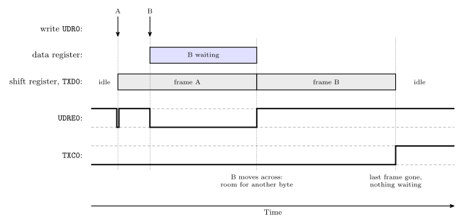
Figure 59: Sending two bytes, A then B, one straight after the other. A moves from the data register into the shift register as soon as it is written, so UDRE0 drops only for an instant and B can be written while A is still on the wire. B then waits in the data register, UDRE0 staying at 0, until A’s stop bit has gone, when it moves across and UDRE0 returns to 1. TXC0 is set only at the very end: the last frame has left and no byte is waiting behind it.
- Use data register empty to keep data flowing: each time it fires, hand over the next byte.
- Use transmit complete when the program needs to know the line has gone quiet, for example before switching the transmitter off.
Receiving by interrupt. The handler runs once per byte, and reading UDR0 is what clears the flag:
#include <avr/io.h>
#include <avr/interrupt.h>

ISR(USART0_RX_vect) {
    uint8_t c = UDR0;                     /* reading clears RXC0             */
    UDR0 = c;                             /* echo (assumes room, see below)  */
}

int main(void) {
    UBRR0  = 51;
    UCSR0B = (1<<RXEN0) | (1<<TXEN0) | (1<<RXCIE0);
    sei();
    while (1) {
        /* free to do anything else */
    }
}
A handler that does not read UDR0 leaves RXC0 set, and it is called again the moment it returns, for ever. The echo here is safe because bytes cannot arrive faster than they can be sent back at the same baud rate.
UDRIE0 needs care. The data register is empty most of the time, so its flag is nearly always set. Enabling the interrupt with nothing to send calls the handler continuously. The pattern is to enable UDRIE0 when there is data queued and have the handler disable it again when the queue runs out.
Common mistakes
- Reading
UDR0to see what was written. Reads and writes go to different registers. - Forgetting
RXEN0orTXEN0. The baud rate and format can be perfect and nothing happens. - Forgetting the \(-1\) in the baud-rate formula, giving 52 for 9600 instead of 51.
- Writing
UDR0without checkingUDRE0, which loses bytes when sending more than one. - Reading
UDR0before the error flags. The flags belong to the byte being read and are gone afterwards. - A receive handler that does not read
UDR0. - Leaving
UDRIE0enabled with nothing to send. - Mismatched settings at the two ends. The symptom is garbled characters, not silence (serial-communication).
See also
- serial-communication — frames, parity, sampling, baud rate against bit rate, RS232
- avr-interrupts — flags, enables, the vector table and writing a handler in C
- polling-and-interrupts — waiting on a flag against being interrupted by it
- avr-timers-and-counters — the master formula the baud-rate formula mirrors
- shift-registers — the heart of the transmitter and the receiver
- bit-masking · c-preprocessor-and-avr-headers —
(1<<RXEN0)and where the names come from - io-board — the USB-serial device at the other end of the wires
- avr-spi — the SPI port, and the USART as an SPI master when
UMSELn1:0=11 - 2026-09-24-serial-io — Lecture 18
Bit Masking
Using a bitwise operation against a constant mask to touch only the bits you care about, leaving the rest alone. See boolean-algebra for the underlying laws and avr-instructions for the instructions used here. The same masks, written from the bit names in the AVR’s header files, are how every I/O register is set up in C: see set, clear and toggle and writing register bits by name.
Sometimes you are interested in only a few bits of a register. A bitwise AND can mask out the bits that are not of interest — and more generally, masking can selectively set, clear, toggle or extract bits.
The reason any of this is possible is that a bitwise instruction is not one eight-bit operation. It is eight independent one-bit operations running in parallel, and the two operands’ bit \(i\) decide result bit \(i\) with no reference to any other column.
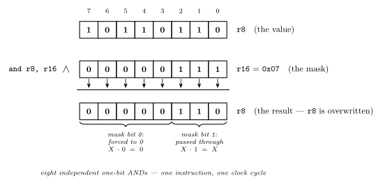
Figure 60: Why a mask works, one column at a time. Two rows of bits, an arrow down out of each column into a result row that overwrites the destination: here and r8, r16 with the mask 0x07, extracting the low three bits. The eight columns never interact — one mask bit decides one result bit, a 1 passing the value’s bit through and a 0 forcing it to zero — and all eight happen at once in a single instruction. Choosing a mask is therefore nothing more than deciding, position by position, which bits to keep.
Read Figure 60 column by column and the technique stops needing to be memorised: since the columns are independent, choosing a mask is just choosing, for each of the eight positions separately, whether that position gets passed through or forced.
The three identities that make it work
Each of AND, OR and XOR has a value that passes a bit through unchanged and a value that forces it. That pairing is the whole technique.
| \(X \cdot 0\) | \(X \cdot 1\) | \(X \cdot X\) | |
|---|---|---|---|
| AND | \(= 0\) | \(= X\) | \(= X\) |
| \(X + 0\) | \(X + 1\) | \(X + X\) | |
|---|---|---|---|
| OR | \(= X\) | \(= 1\) | \(= X\) |
| \(X \oplus 0\) | \(X \oplus 1\) | \(X \oplus X\) | |
|---|---|---|---|
| XOR | \(= X\) | \(= \overline{X}\) | \(= 0\) |
Reading off the pass-through and force columns gives the operation to reach for:
| To do this to the selected bits | Use | Mask bit = 1 on | Mask bit = 0 on |
|---|---|---|---|
| Clear them to 0 | AND |
the bits to keep — \(X \cdot 1 = X\) | the bits to clear — \(X \cdot 0 = 0\) |
| Set them to 1 | OR |
the bits to set — \(X + 1 = 1\) | everything else — \(X + 0 = X\) |
| Toggle them | EOR |
the bits to flip — \(X \oplus 1 = \overline{X}\) | everything else — \(X \oplus 0 = X\) |
| Extract them (others zeroed) | AND |
the bits to keep — \(X \cdot 1 = X\) | the bits to discard — \(X \cdot 0 = 0\) |
Note the asymmetry: AND’s mask is 1 on the bits you keep, whereas OR’s and XOR’s masks are 1 on the bits you act on. Getting that backwards is the usual bug — with AND you write the mask for what survives, with the other two for what changes.
\(X \oplus X = 0\) is the other one worth remembering: XORing a register with itself is the cheapest way to zero it.
In AVR assembly
The masks are ordinary constants, so the bitwise instructions of avr-instructions do the work. On AVR the immediate forms (andi, ori) only reach r16–r31; for a low register, load the mask into a high register and use the two-register form.
Extract the least significant three bits of r7 into r8, other bits of r8 zero.
    mov  r8, r7          ; copy the source
    ldi  r16, 0x07       ; mask 0000 0111 — keep the bottom three
    and  r8, r16         ; everything else forced to 0
Toggle the most significant four bits of r9, other bits unchanged.
    ldi  r16, 0xF0       ; 1111 0000 — flip the top four
    eor  r9, r16         ; bottom four XOR 0, so unchanged
Clear the least significant four bits of r10, other bits unchanged.
    ldi  r16, 0xF0       ; 1 on the bits to KEEP
    and  r10, r16        ; bottom four AND 0 -> 0
Set the most significant four bits of r11 to 1, other bits unchanged.
    ldi  r16, 0xF0       ; 1 on the bits to set
    or   r11, r16        ; bottom four OR 0, so unchanged
Note how 0xF0 appears as the mask in three of these with three different meanings — keep, flip, set — decided entirely by the instruction it is paired with.
In C
The same four operations with C’s bitwise operators (c-operators), which is how every AVR C program touches its ports. The masks are the same; the immediate-register restriction disappears, since the compiler chooses the registers.
| Operation | Operator | Example | Reads as |
|---|---|---|---|
| Clear particular bits | & with 0s on the bits to clear |
var = PINB & 0x0F; |
keep the low nibble, zero the high |
| Test particular bits | & with a 1 on the bit to test |
if (PINB & 0x02) … |
true if bit 1 is set |
| Set particular bits | \| with 1s on the bits to set |
PORTC = PINB \| 0x80; |
force bit 7 to 1 |
| Invert particular bits | ^ with 1s on the bits to flip |
PORTC = PINB ^ 0x0F; |
flip the low nibble |
Write the mask as a shift, not a hex constant: (1<<5) says bit 5 where 0x20 has to be decoded, and the header files name every register bit as a bit number for exactly this use (c-preprocessor-and-avr-headers):
DDRB  = (1<<5);                 /* bit 5 output, every other bit input: REPLACES the register */
DDRB |= (1<<4) | (1<<3);        /* bits 3 and 4 output, the rest unchanged: read-modify-write */
DDRB &= ~(1<<3);                /* bit 3 back to input, the rest unchanged                    */
PORTC ^= (1<<0);                /* toggle bit 0                                              */
TCCR1B = (1<<WGM12) | (1<<CS11) | (1<<CS10);   /* named bits, ORed into one value            */
The difference between the first two lines is the one that bites: = writes the whole register and silently sets the other seven bits to 0, |= ORs into what is already there. In assembly the second line is three instructions — in, ori, out — and the C compiler emits exactly those (week8-lab-avr-c-programming). For a single-bit clear the mask is the complement of the set mask, ~(1<<n), which is why clear bit 3 is &= ~(1<<3) and not &= (1<<3).
The test idiom needs no comparison. PINB & 0x02 is 0x02 when bit 1 is set and 0 when it is not, and C treats any non-zero value as true (c-control-flow) — so if (PINB & 0x02) is right and if ((PINB & 0x02) == 1) is always false, because the masked value is 2, never 1.
Set, clear and toggle on an I/O register
Changing one bit of an I/O register, and only that bit, is one of three lines. Each reads the register, combines it with a one-bit mask and writes it back:
| To | Write | The mask | Why the other bits survive |
|---|---|---|---|
| set bit n | REG \|= (1<<n); |
a 1 on bit n | \(X + 0 = X\) |
| clear bit n | REG &= ~(1<<n); |
a 0 on bit n, 1s elsewhere | \(X \cdot 1 = X\) |
| toggle bit n | REG ^= (1<<n); |
a 1 on bit n | \(X \oplus 0 = X\) |
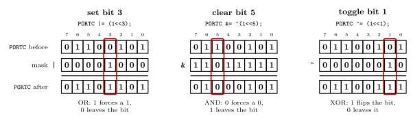
Figure 61: Set, clear and toggle on one register byte. Each panel starts from the same value of PORTC, 0110 0101, and changes one bit, outlined, with a single read-modify-write. The mask is a 1 shifted to the bit’s position, complemented for a clear. In every other column the mask holds the value that leaves a bit alone: 0 for OR and XOR, 1 for AND. Set gives 0110 1101, clear gives 0100 0101 and toggle gives 0110 0111, and each time the other seven bits are untouched.
Toggle is not enable. TIMSK2 ^= (1<<OCIE2A); turns the timer 2 compare A interrupt on only if it was off, and a second run turns it off again. To enable whatever the bit was before, set it with |=; to disable, clear it with &= ~. Toggling is for things meant to alternate, like an LED blinking.
The register has to be one that stores what is written. PORTx and DDRx do. PINx does not: it reads the pins, and on the ATmega324A a 1 written to one of its bits toggles the matching PORTx bit, so a read-modify-write on PINx changes the wrong bits (avr-io-ports).
Writing register bits by name
When setting or clearing bits of an I/O register, be explicit about which bits. Three ways to write the same value, from worst to best:
TCCR1B = 10;                          /* poor:   a number                    */
TCCR1B = 0x0A;                        /* better: the pattern, 0000 1010      */
TCCR1B = (1<<WGM12) | (1<<CS11);      /* best:   the bits, by name           */
WGM12 is bit 3 of TCCR1B and CS11 is bit 1, so all three are 0000 1010. Only the last says which bits, so a reader can check them against the datasheet without decoding anything: CTC mode, clock divided by 8 (avr-timers-and-counters). It costs nothing, either. The compiler works out (1<<WGM12) | (1<<CS11) while compiling, and all three lines become the same instructions.
The names are bit numbers. The device header that <avr/io.h> includes defines every bit name as the bit’s position in its register:
#define WGM02 3A name is not a mask; 1<< makes it one (c-preprocessor-and-avr-headers). The names are the datasheet’s, and the datasheet has errors in places, so the I/O register summary at the back is the one to check a name against.
Assembly uses the same names. In ldi r16, (1<<WGM02)|(1<<CS01) the assembler works out the constant, 0x0A, and the instruction stored is ldi r16, 0x0A.
A name belongs to one register. WGM12 and WGM02 are both 3, so (1<<WGM12) written into TCCR0B sets WGM02, and the compiler cannot notice, because all it sees is the number 3. Pair each name with the register whose datasheet entry defines it. The same byte 0x0A is CTC mode in TCCR1B and a reserved mode in TCCR0B (2026-10-05-more-io).
Masking sets the status flags too
Status register flags will be set also — a mask operation is a real ALU operation, not a free one. AND, OR and EOR all clear V and set N and Z from the result (C is untouched); see avr-architecture.
That side effect is often the actual point. andi r16, 0x01 keeps only bit 0, so:
\[Z = 1 \iff \text{bit 0 of } \texttt{r16} \text{ is } 0 \iff \texttt{r16} \text{ is even}\]
which makes a single masked AND an even/odd test. Any single-bit mask turns the Z flag into a test of that one bit — and tst rd, which is just and rd, rd, is the degenerate case that tests the whole register against zero.
Common mistakes
&= (1<<n)to clear bit n. That keeps bit n and clears the other seven. A clear’s mask is the complement,~(1<<n).=where|=was meant.DDRB = (1<<5)makes PB5 an output and every other pin of port B an input.- A bit name without the shift.
TCCR1B |= WGM12;ORs in the number 3,0000 0011, which setsCS11andCS10, clock divided by 64, and leavesWGM12alone. - A bit name in the wrong register.
(1<<WGM12)inTCCR0BsetsWGM02. ^=to enable. A toggle enables only from off; run twice, it disables.- A read-modify-write on
PINx. WritingPINxtoggles outputs, so it cannot clear or set a bit. - Getting AND’s mask backwards. With AND the 1s mark the bits to keep; with OR and XOR they mark the bits to change.
if ((x & mask) == 1). The masked value is the mask’s own value, so the test is false unless the mask is bit 0. Test for non-zero.
See also
- boolean-algebra · avr-instructions · avr-architecture
- avr-io-ports — one bit of a port in C and assembly, and why
PINxis different - avr-timers-and-counters — the
TCCRnBfields named in the examples - 2026-10-05-more-io — Lecture 19: poor, better and best,
TIMSK2toggled - week5-lab-avr-assembly-one — Lab 9, where these snippets are the exercise
- week8-lab-avr-c-programming — Lab 11, the same operations in C · c-operators · c-preprocessor-and-avr-headers
C Preprocessor and AVR Headers
The preprocessor — #include and #define — and the three lines of avr/io.h that let DDRA = 0xFF; be written as if a hardware register were a variable. First met in 2026-09-10-more-c-programming-on-the-avr; the port registers themselves are in avr-io-ports.
What the preprocessor is
C programs are first parsed by a preprocessor, which replaces preprocessor directives with substitute text. Only then does the compiler see the program. Directives start with #:
| Directive | Does |
|---|---|
#include … |
paste in a file |
#define … |
define a macro — a textual substitution |
#if, #ifdef, #else, #undef, … |
conditional inclusion, un-definition, and others |
The preprocessor does not know C. It edits text. Whatever it produces is what the compiler compiles, and every surprise in this note comes from forgetting that.
#include
| Form | Kind of header | Looks in |
|---|---|---|
#include <filename.h> |
system | the system include directories — where avr/io.h and stdio.h live |
#include "filename.h" |
user-defined | your own project directory first |
The directive is replaced by the whole contents of the named file, at that point. After preprocessing there is one file, with the header pasted in at the top.
Header files
Header (.h) files are used for common macros, function prototypes etc — the C counterpart of m324Adef.inc in assembly (avr-io-ports).
stdio.h— prototypes ofprintf()etc. The AVR has a simplified version (no files);printf()only works if you say where the characters go, e.g. a serial port.avr/io.h— defines the AVR’s useful constants and functions/macros. Definitions depend on the actual device targeted: it reads which chip is being compiled for and pulls in that chip’s register map, soDDRAmeans the right address for the ATmega324A and a different one for another part. It also suppliesuint8_tand the other fixed-width types.
Every program in the course starts with #include <avr/io.h>.
Headers against libraries
A header file is not the library. A header
- defines useful preprocessor macros,
- declares the functions that are in the library, as function prototypes, and
- declares variables that are available externally, with
extern.
The library is the collection of object files that implements the functions (compilation-and-linking).
A prototype such as int printf(const char *fmt, ...); tells the compiler the name, the argument types and the return type. That is enough for the compiler to check a call and generate it. There is no code in it, so in main.o the call to printf is left as an external reference. The code is in the library, an object file printf.o inside it, and the linker joins it on and fills in the address. An extern declaration does the same for a variable: extern int count; says that count exists somewhere else and reserves nothing.
So the header goes to the compiler, through the preprocessor, and the library goes to the linker. The two kinds of mistake show up at different steps:
| Missing | Shows up when | Typical message |
|---|---|---|
the #include |
compiling | implicit declaration of function printf |
the library, or the .c file that defines the function |
linking | undefined reference to printf |
Figure 62: Where a header and a library each come into play, for a program that calls printf. The header holds only declarations. The preprocessor pastes it into main.c so that the compiler can check and generate the call, and in main.o that call is still an external reference. The library holds the definitions, as already compiled object files with an index. The linker finds printf.o through the index, links it in, and fills in the call. The header is used by the compiler and the library by the linker.
#define — macros
Macros are textual substitutions.
| Macro | Effect |
|---|---|
#define pi 3.1415 |
every later pi becomes 3.1415 — A = pi * r²; becomes A = 3.1415 * r²; (the superscript is shorthand; in real C the square would be r * r) |
#define EVER ;; |
for(EVER) becomes for(;;), an infinite loop |
#define sum(a,b) (a+b) |
a macro with parameters: sum(x, 2) becomes (x+2) |
A macro with parameters looks like a function call and is not one: no call happens, the arguments are pasted into the body as text, and the result is compiled in place.
The SQUARE trap
Given
#define SQUARE(x) (x*x), what isSQUARE(1+2)?
5, not 9. Paste the text: (1+2*1+2). Multiplication binds tighter than addition, so it is \(1 + 2 + 2\). The argument was never evaluated first, because there is no function to evaluate it.
The fix is parentheses around every parameter, and around the whole body:
#define SQUARE(x) ((x)*(x)) /* SQUARE(1+2) -> ((1+2)*(1+2)) = 9 */The outer pair matters as much as the inner: without it, 1 / SQUARE(a) becomes 1 / (a)*(a), which is \(a\), not \(1/a^2\). Write every macro this way. The AVR headers below do — note the brackets around (mem_addr) and (io_addr).
A second pitfall: an argument with a side effect is pasted as many times as the parameter appears. SQUARE(i++) becomes ((i++)*(i++)) and increments i twice.
The avr/io.h register macros
The definitions behind the port names, from avr/io.h and the device header it includes:
#define _MMIO_BYTE(mem_addr) \
                (*(volatile uint8_t *)(mem_addr))
#define _SFR_IO8(io_addr) \
                _MMIO_BYTE((io_addr) + 0x20)

/* Input Pins, Port A */
#define PINA      _SFR_IO8(0x00)

/* Data Direction Register, Port A */
#define DDRA      _SFR_IO8(0x01)

/* Data Register, Port A */
#define PORTA _SFR_IO8(0x02)(\ at the end of a line continues a directive onto the next line.)
Upshot: I/O register names can be used as variables.
DDRA = 0xFF;
PORTA = PINC | 0xF0;
Unrolling DDRA
| Step | Text |
|---|---|
| as written | DDRA = 0xFF; |
#define DDRA |
_SFR_IO8(0x01) = 0xFF; |
#define _SFR_IO8 |
_MMIO_BYTE((0x01) + 0x20) = 0xFF; |
#define _MMIO_BYTE |
(*(volatile uint8_t *)((0x01) + 0x20)) = 0xFF; |
Reading the final line from the inside out:
(0x01) + 0x20is0x21— a number.(volatile uint8_t *)casts it: treat this number as the address of an 8-bit unsigned byte. Now it is a pointer (c-pointers-and-arrays).- The leading
*dereferences it: the byte at that address. = 0xFFstores into that byte.
So DDRA = 0xFF; is a store to data address 0x21, and x = PINC; is a load from data address 0x26. There is no variable called DDRA anywhere; the name dissolves before the compiler sees it.
Why + 0x20
The AVR’s 64 I/O registers have two addresses each (avr-io-ports): an I/O-space number 0–63, which is what in and out use, and a data-space address 0x20 higher, where lds/sts — and any C pointer — find the same register. DDRA is I/O 0x01 and data 0x21. The macro takes the I/O number the datasheet lists and adds the offset, because a C pointer can only name data-space addresses. (The compiler, seeing a constant address in the I/O range, will usually emit in/out anyway.)
Why volatile
volatile tells the compiler the value at this address can change without the program changing it, and that every read and write matters. Without it the compiler is entitled to assume that a byte it wrote a moment ago still holds what it wrote, and that two reads with nothing between them give the same answer — both false for a port: PINC changes whenever the pins do, and PORTA is written for its effect on the pins, not to be read back. volatile forbids the optimisations that would break that. It is the one piece of the macro that is about hardware rather than addressing.
The same keyword belongs on any ordinary variable that an interrupt handler writes. To the code in main, a handler’s write is as invisible as a pin changing, and for the same reason: nothing in main’s own flow of control explains it. See avr-interrupts.
Naming bits
The headers also define bit numbers for every flag and pin — for example FLAG_NAME == 5 — so a mask is written from a name rather than a constant:
1 << FLAG_NAME              /* 00100000 when FLAG_NAME is 5 */
PORTA |= (1 << 5);          /* set one bit                   */
PORTA &= ~(1 << 5);         /* clear one bit                 */
The shift and the |=/&= shorthands are in c-operators; the mask patterns are in bit-masking. FLAG_NAME is a placeholder name; the actual names for the ATmega324A’s pins and flags come from the device header, as #define WGM02 3 does in 2026-10-05-more-io.
See also
- avr-io-ports — the port registers, and the I/O-space versus data-space address columns
- c-pointers-and-arrays — what
*(uint8_t *)addrmeans - c-operators —
1 << n,|=,&= - bit-masking · memory-models
- avr-interrupts —
volatileon variables shared with an interrupt handler - compilation-and-linking — what happens after the preprocessor: object files, libraries and the linker · 2026-10-15-compilation-and-linking — Lecture 22
- 2026-09-10-more-c-programming-on-the-avr — Lecture 14
The I/O Board
The I/O board in the lab kit carries the input and output devices you wire your breadboard circuits to, for experimenting with simple digital circuits. It plugs directly onto the breadboard, and adds a logic probe for debugging and a UART serial interface for talking to other devices.
It is powered from a single USB connection and has current-sense circuitry that detects short circuits and protects your designs.
Pin numbers for every device are in device-pinouts; the kit itself is loaned out in week3-lab-logisim-and-flip-flops. Two more parts of the kit that are used alongside the board, the joystick and the LED matrix, are described at the end.
What’s on it
| 1. USB connector | 2. Power LED | 3. Power switch | 4. 7-segment display |
| 5. Switches | 6. LEDs | 7. Buttons | 8. UART transmit/receive LEDs |
| 9. Logic probe indicator LEDs | 10. Fault LED | 11. VCC / GND headers | 12. I/O device headers |
| 13. Auxiliary power connector | 14. High current mode jumper |
Items 13 and 14 are the auxiliary power connector and the high-current-mode jumper. The one extra power connection the labs use is connector J1, which powers the LED matrix in Lab 16 (below).
The board at a glance
The board is a C shape: a left-hand spine carrying the USB connector, the power switch, the two status LEDs and the seven-segment display, plus a top arm and a bottom arm that straddle the breadboard’s central channel. All the I/O devices come out on the two 16-pin headers on the inner edges of those arms, and every device is reached through the column of breadboard holes directly above or below its printed label.
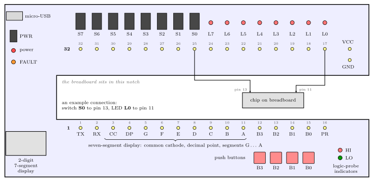
Figure 63: A plan view of the board, not to scale, with the parts on the left spine placed roughly. Each I/O device sits on one pin of one of the two 16-pin headers, and the column of breadboard holes at that pin is how you reach it. The board itself prints only the two end markers, a bold 32 at the left of the top header and a bold 1 at the left of the bottom one. The small numbers at the other pins are their pin numbers, the ones a schematic uses. The connection drawn in the notch is an example: switch S0 to pin 13 of a chip, LED L0 to pin 11.
Two things about the numbering are worth fixing in your head before you wire anything:
- The top header counts down, left to right. Its leftmost pin is 32 and its rightmost is 17, so the switches run
S7…S0and then the LEDsL7…L0as you read left to right. That is the opposite of the reading order you would guess from the pin numbers alone. - The bottom header counts up, left to right, pin 1 to pin 16:
TX RX CC DP G F E D C B A B3 B2 B1 B0 PR. The middle nine of those are the seven-segment display —CCits common cathode,DPits decimal point, andGdown toAits seven segments — which is why nine consecutive pins carry single-letter names.
VCC and GND pads sit at the far right of both arms, which is where the breadboard’s power rails get fed from.
Setup
Insert the board into the breadboard, aligning the downward-facing headers with the right holes.
If aligned correctly, the I/O board should not require excessive force to insert.
Connect a micro-USB cable to the connector at the top-left corner.
DO NOT STORE THE BOARD WITH THE USB CABLE ATTACHED — THIS MAY CAUSE THE USB CONNECTOR TO BREAK OFF!!
The USB connector is the part people break.
Turn the board on by sliding the PWR switch up to ON; the red power LED should light. Then check the orange FAULT LED does not light. If it does, power off immediately.
The fault LED
The board uses a current-limited power switch to protect itself and anything it powers from short circuits. A short lights the orange FAULT LED.
If it’s on: push PWR down to OFF immediately, and check your design for shorts before restoring power.
WARNING! In the case of a short circuit, the current-limiting switch may become extremely hot.
The logic probe
Attach a wire to the column of terminals above the PR label — pin 16, the rightmost pin of the bottom header. Touch the free end to any point in the circuit and the HI / LO LEDs show the logic state there.
As circuits increase in complexity, so does the necessity of having a clear strategy — probing random points in a large circuit rarely reveals the location of errors.
Suggested troubleshooting strategy
- Check the FAULT light is not on, which would indicate a short circuit.
- Probe VCC and GND at every device in your circuit, to confirm each one is actually powered.
- Start at the inputs and move logically through to the outputs. Pen and paper helps: write down the expected state at each point first, then verify it with the probe. A schematic and a truth table are great for this.
The key to any successful debugging strategy is to assume nothing, know what to expect before you begin testing, and have a plan.
Step 2 is the one worth internalising — an unpowered chip looks exactly like a wrong-logic chip until you probe its power pins, and grouped VCC/GND entries on a schematic (see circuit-schematics) make it easy to forget one.
Electrical characteristics
| VCC | 5 V |
| GND | 0 V |
| Logic high | > 3.5 V |
| Logic low | < 1.5 V |
The gap between 1.5 V and 3.5 V is undefined, which is why a floating pin can read as either (week3-lab-logisim-and-flip-flops). What the logic probe shows for a voltage inside that band is not documented.
The joystick
The kit’s two-axis joystick is a small board of its own, made to sit in the breadboard next to the I/O board. Each axis is a potentiometer between its own supply pin and ground, and the stick moves the wiper. So each axis gives a voltage that follows the stick across its travel, from 0 V at one side to 5 V at the other, for the A/D converter to read (analog-to-digital-conversion).
| Pin | What it is | Connect to |
|---|---|---|
| L/R+ | top of the left-right potentiometer | VCC |
| U/D+ | top of the up-down potentiometer | VCC |
| GND ×2 | bottom of both | GND, either one |
| L/R ×2 | x: 0 V with the stick to the left, 5 V to the right | an analog input, either one |
| U/D ×2 | y: 0 V at the bottom, 5 V at the top | an analog input, either one |
- The doubled pins are joined on the board. One wire to each of L/R, U/D and GND is enough.
- The two
+pins are separate. Both have to go to VCC, or one axis has nothing to divide. - Left, right, up and down are the joystick’s own, marked by the X and Y arrows printed on it. Placed at the right-hand end of the breadboard, with room for the microcontroller board and programmer to its left, the X arrow points to the top of the breadboard and the Y arrow to the left.
- A potentiometer’s wiper is a weak source. Anything that draws current from it, an LED for instance, pulls its voltage away from the stick’s position. LEDs make a quick wiring test, but they must come off before the converter is used.
- Keep the black foam that protects the pins when the joystick is put away.
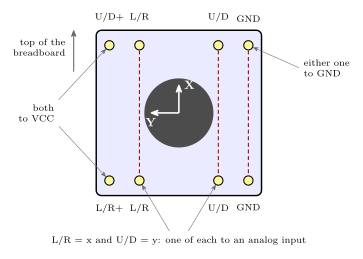
Figure 64: The joystick’s eight pins, seen from above with the board placed as it sits in the breadboard, its X arrow pointing to the top. The pins near each corner come in twos. The dashed lines join the pins that are connected on the board itself: the two L/R pins, the two U/D pins and the two GND pins, so one wire to each pair is enough. The two supply pins, U/D+ at the top left and L/R+ at the bottom left, are not joined, and both go to VCC. L/R carries x and U/D carries y to the analog inputs.
The LED matrix
The LED matrix is a display of 16 columns by 8 rows, each pixel a red LED and a green LED together. It is driven over SPI: the AVR is the master and the matrix a slave that takes commands one byte at a time (avr-spi).
Connecting it
It has two headers:
- K1, two pins, is its power. A two-wire lead joins it to the I/O board’s connector J1, VCC on J1’s left pin and GND on its right.
- K2, four pins, is the SPI connection, to the AVR’s SPI port on PB7 to PB4: SCK on PB7, MISO on PB6, MOSI on PB5 and \(\overline{\text{SS}}\) on PB4. Match the order of the pins on K2 against the datasheet before plugging the lead in.
The Err state. PB7 to PB5 are also the pins the programmer uses to load the AVR, so programming sends the matrix a stream of what look to it like garbage commands, and it can show Err. Holding the AVR’s reset button down for at least half a second after programming clears it before the program starts.
What to send it
Every message starts with a command byte. Two commands are enough to draw anything:
| Command | Bytes | Does |
|---|---|---|
| clear | 0x0F |
every pixel off |
| set one pixel | 0x01, position, colour |
sets one pixel to a colour |
- Position byte:
(y << 4) | x. The row y, from 0 at the bottom to 7 at the top, is the high nibble. The column x, from 0 at the left to 15 at the right, is the low nibble. - Colour byte:
(green << 4) | red. Each nibble is a brightness from 0 to 15. Red alone is0x0F, green alone0xF0, both full is yellow,0xFF, and full red with half green is orange,0x7F.
The matrix’s reference manual is the full description of the commands it accepts.
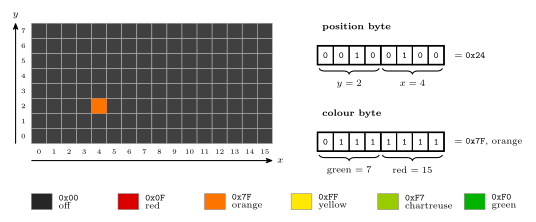
Figure 65: How a pixel is addressed and coloured. The matrix is 16 columns, x from 0 to 15 left to right, by 8 rows, y from 0 to 7 bottom to top. A position byte puts y in its high nibble and x in its low one, so the pixel at x = 4, y = 2 is 0x24. A colour byte puts the green brightness in its high nibble and the red in its low one, each 0 to 15. The swatches show what some colour bytes look like: the colours here are the light from the red and green LEDs mixed.
Lab 16 works through the commands and uses them for a demo, a scrolling marquee across two matrices and an Etch-A-Sketch (week10-lab-adc-and-spi).
See also
- device-pinouts — the pin table behind Figure 63, and the board’s schematic symbols
- circuit-schematics — how the board is drawn on a schematic (
IO1/IOBOARD, input and output pentagons) - avr-io-ports — the same switches and LEDs driven from an AVR rather than from gates
- week3-lab-logisim-and-flip-flops — where the kit is loaned out
- week10-lab-adc-and-spi — Lab 16: the joystick read by the A/D converter, and the LED matrix driven over SPI
- analog-to-digital-conversion · avr-spi — the two AVR peripherals the joystick and the matrix are used with
Memory Models
The first of the four things that make up an ISA (instruction-set-architecture): how memory looks to the CPU. Four issues decide that — addressable cell size, alignment, address spaces and endianness — and every one of them is a decision the specification has to make, not something the hardware settles on its own.
Memory as addressable cells
Computer memory is conceptually a set of addressable cells:
- Each cell has a unique address (or cell number).
- Cells are usually 8 bits wide (i.e. hold one byte).
- Various cell widths have been used in the past — 8 bits is a convention, not a law.
Drawn as a table, the address indexes the rows and the cell width is how wide each row is:
| Address | ← cell width → |
|---|---|
| 0 | |
| 1 | |
| 2 | |
| 3 | |
| … |
A “4 × 3 memory” in that notation means 4 addresses of 3-bit cells — and \(4 = 2^2\), so two address bits. Built at gate level, it shows that “memory” at this level is nothing more exotic than flip-flops-and-latches and combinational-logic-blocks arranged into storage.
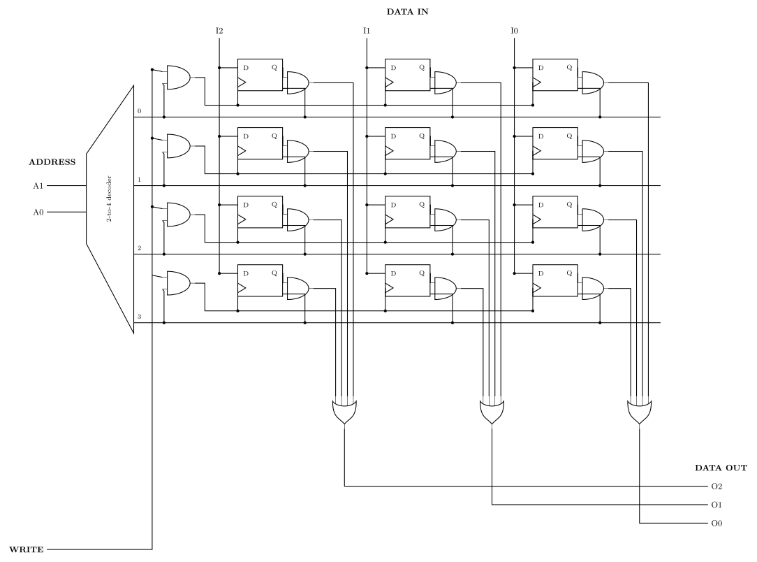
Figure 66: A 4 × 3 memory at gate level — four addresses of three-bit cells. Twelve D flip-flops in four rows of three: one row is one addressable cell. The decoder turns A1 A0 into exactly one row-select (word) line. Writing: the word line ANDed with WRITE clocks that row’s three flip-flops, so DATA IN (I2 I1 I0) — which is wired to every row’s D inputs all the time — is captured only by the selected row. Reading: each flip-flop’s Q is ANDed with its own word line and the three cells of a column are OR’d together, so the unselected rows contribute 0 and DATA OUT (O2 O1 O0) carries the selected row alone. The decoder is drawn as a trapezoid with the wide edge on the right, and the flip-flops as plain rectangles with a clock wedge on the lower-left edge, per this course’s conventions (csse2010-diagram-notation). The most significant bit, I2/O2, is the leftmost column.
A. Addressable cell size
Most common cell size is 8 bits (1 byte) — but not always.
The AVR is the counterexample sitting on the bench:
| AVR memory | Cell width |
|---|---|
| Data memory | 8 bits |
| Instruction (program) memory | 16 bits |
Which is why an AVR instruction is “one word” rather than “two bytes” — a program-memory address counts 16-bit cells.
The bus transports the content of a cell, but the data bus may be wider than one cell: it can retrieve several cells (addresses) at once. When it does, the address bus does not need to be as wide.
Bus sizes
For every doubling of the data bus width, remove the least significant bit of the address bus.
For a memory of \(2^n\) cells at 8 bits per cell — so an address size of \(n\) bits:
| Data bus | Address bus | Cells per transfer |
|---|---|---|
| 8 bits | \(n\) bits | one cell at a time |
| 16 bits | \(n-1\) bits | two cells at a time |
| 32 bits | \(n-2\) bits | four cells at a time |
The reason is that a wide transfer always moves an aligned group of cells. With a 16-bit data bus the memory only ever hands over cell pairs \((0,1), (2,3), (4,5), \dots\) — so the bottom address bit never selects anything, and naming the pair takes one bit fewer than naming the cell.
Worked example. A memory of 64 cells, 8 bits each, addressed 000000 … 111111:
\[64 = 2^6 \text{ cells} \implies 6\text{-bit addresses}\]
| Data bus | Address bus |
|---|---|
| 8 | 6 |
| 16 | 5 |
| 32 | 4 |
Read the two buses as a pair, not separately: widening one narrows the other by exactly as much.
Word addresses and byte addresses
The AVR’s 16-bit program-memory cells have one practical consequence. The program counter, jmp, call and every code label count words. But a table of constant bytes kept in flash is read a byte at a time by lpm, load program memory, and lpm takes a byte address in the Z register. Word \(w\) holds bytes \(2w\) and \(2w + 1\), with the low byte at the even address, which is the AVR being little endian (section D).
So turning a code label into a byte address means doubling it. Take the string Hello stored at word 2 by mesg: .db 72,101,108,108,111 (assembly-process):
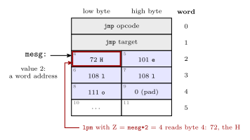
Figure 67: One region of program memory addressed two ways. Each row is a 16-bit word, numbered on the right, and each half is a byte, numbered inside its cell. The label mesg has the value 2 because labels in the code segment count words. Byte addressing counts the halves, low byte first, so word 2 starts at byte 4. That is why lpm is pointed at mesg*2: with Z = 4 it loads 72, the H. The five bytes of the string take two and a half words, and the last half word is a zero pad. Grey marks the jmp, blue the string and red the byte that lpm reads.
        ldi  ZH, high(mesg*2)   ; Z = 4: byte address of word 2
        ldi  ZL, low(mesg*2)
        lpm                     ; r0 <- 72, the H
Leaving out the *2 points Z at byte 2, the low byte of word 1, which is half of the jmp.
B. Alignment
Many architectures require natural alignment, e.g.
- 4-byte words starting at addresses 0, 4, 8, …
- 8-byte words starting at addresses 0, 8, 16, …
i.e. an \(n\)-byte value must start at an address that is a multiple of \(n\).
Taking an 8-byte word on a machine that fetches 8 bytes at a time:
| Where it sits | Reads needed | |
|---|---|---|
| Aligned | bytes 8–15, i.e. an 8-byte word at address 8 | 1 — it is exactly one fetched block |
| Non-aligned | bytes 12–19, i.e. an 8-byte word at address 12 | 2 — the top half of block 8–15, plus the bottom half of block 16–23 |
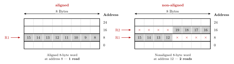
Figure 68: An aligned and a non-aligned 8-byte word. Four blocks of eight bytes; grey marks the bytes of the 8-byte word. On the left the word starts at address 8, so it is one block — one read. On the right it starts at address 12, so it takes the top half of the block at 8 and the bottom half of the block at 16 — two reads, marked R1 and R2. Two things about the drawing: addresses increase upward (unlike every other memory figure in the course, where they increase downward — see csse2010-diagram-notation on that inconsistency), and byte numbers within a row run high-to-low left to right. The × marks a byte in the fetched block that is not part of the word.
Alignment is often required because it is more efficient — the aligned case is always one read, the non-aligned case sometimes two, and the hardware that stitches two blocks together and extracts the middle is hardware that a machine demanding alignment simply does not need.
When alignment is not required — the Pentium IV
- Fetches 8 bytes at a time from memory (64-bit wide data bus).
- Alignment is NOT required, so the processor stays backwards compatible with earlier processors.
- A 4-byte word stored at address 4 takes 1 read (bytes 0 to 7).
- A 4-byte word stored at address 6 must read bytes 0 to 7 (one read) and bytes 8 to 15 (second read), then extract the 4 required bytes from the 16 bytes read.
Counting reads in general
A data bus \(w\) bytes wide delivers one aligned \(w\)-byte block per read. An \(n\)-byte value starting at address \(a\) therefore costs
\[\left\lceil \frac{(a \bmod w) + n}{w} \right\rceil \text{ reads}\]
The best case is \(n/w\) (rounded up), when the value starts on a block boundary; every other starting offset can push it one block further. So a value read from an arbitrary address costs either \(\lceil n/w \rceil\) or one more than that — which is why questions of this shape almost always answer “\(k\) or \(k+1\)” rather than a single number.
Worked example: an 8-byte value on a 16-bit data bus, no natural alignment required. Here \(w = 2\) and \(n = 8\):
| Starting address | Spans | Reads |
|---|---|---|
| Even | 4 aligned 2-byte blocks | 4 |
| Odd | 9 byte-positions, so 5 aligned blocks | 5 |
so the answer is 4 or 5. The odd case is the one to picture: one byte of the value sits alone at the top of the first block and one byte alone at the bottom of the last, and each of those still costs a whole read.
C. Address spaces
Many microprocessors have a single linear memory address space — the von Neumann architecture:
- e.g. \(2^{32}\) bytes numbered from 0 to \(2^{32} - 1\).
- (These may not be bytes — it depends on the addressable cell size.)
- Program and data share the one space.
However, the Harvard architecture has separate address spaces for instructions and data. The same numeric address means a different location depending on which space you are in, and an instruction says which one it means by what instruction it is.
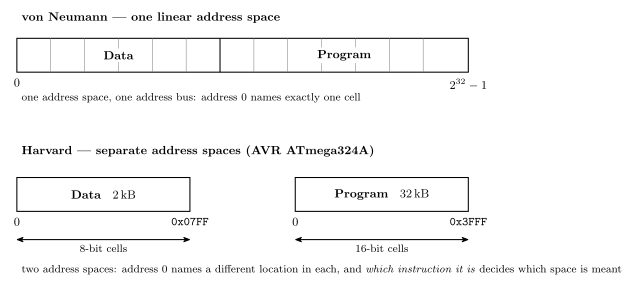
Figure 69: The two address-space models. Above: von Neumann — one linear space, so program and data are separated only by convention and address 0 names exactly one cell. Below: Harvard, in the AVR ATmega324A’s shape — two spaces, each starting at its own 0, with different sizes and different cell widths — and the cell width under each box is the whole reason the arithmetic below works out the way it does: 32 kB of program memory is \(2^{15}\) bytes but only \(2^{14}\) addresses, because each address there names a 16-bit cell. The end addresses follow from the sizes, so the data box ends at 0x07FF (\(2^{11}-1\), for 2048 bytes) rather than the 0x08FF of Figure 70, which is that 2 kB plus the 256 locations in front of it.
AVR ATmega324A is Harvard:
| Space | Size | Address width |
|---|---|---|
| Data | \(2^{11}\) (2048) bytes | 11 bits |
| Instruction | \(2^{14}\) 16-bit words — 16,384 instruction words = 32,768 bytes | 14 bits |
The arithmetic — convert to cells first, then take the logarithm:
\[\text{data: } 2\,\text{kB} = 2 \cdot 2^{10}\,\text{B} = 2^{11} \text{ cells (8-bit)} \implies 11 \text{ bits}\] \[\text{program: } 32\,\text{kB} = 2^{5} \cdot 2^{10}\,\text{B} = 2^{15}\,\text{B} = 2^{14} \text{ cells (16-bit)} \implies 14 \text{ bits}\]
The program-memory step is the one that catches people: 32 kB of flash is only \(2^{14}\) addresses, not \(2^{15}\), because each address names a 16-bit cell. Halve the byte count before taking the log whenever the cells are not bytes.
Laid out as a memory map (see avr-architecture for the rest of the chip):
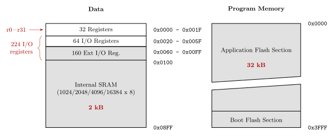
Figure 70: The ATmega324A’s two address spaces. Lowest address at the top, hex addresses outside on the right, grey fill on the coarsely-described regions, and the diagonal break across the flash meaning not to scale: that is this course’s memory-map convention (csse2010-diagram-notation). Marked in red: the register file is r0–r31, the 64 I/O plus 160 extended I/O registers are the 224 of avr-io-ports, the SRAM is 2 kB and the flash 32 kB.
Two details worth pinning down. 0x3FFF \(= 2^{14} - 1\), which is the 14 bits above. And the data space runs to 0x08FF — that is the 2 kB of SRAM plus the 256 locations (0x0000–0x00FF) that the register file and I/O registers occupy in front of it; the “\(2^{11}\) bytes” above is the SRAM itself, which is what the 11 bits size.
The assembler’s view: segments
An assembler treats each address space as a segment with its own location counter (assembly-process). On the ATmega324A there are three, because the EEPROM is a third address space alongside the two above:
| Segment | Directive | Address space | Cell | Counter starts at | The assembler can |
|---|---|---|---|---|---|
| code | .cseg |
program memory, flash, 32 kB | 16-bit word | 0x0000 |
place instructions and constants |
| data | .dseg |
data memory, SRAM | byte | 0x0100 |
only reserve space |
| EEPROM | .eseg |
EEPROM, 1 kB | byte | 0x0000 |
place constants |
Three consequences of separate spaces:
- The same number means different places. Address 0 is the reset
jmpin the code segment, registerr0in data memory and the first EEPROM byte in the EEPROM segment. - The units differ.
.org 0x0100in the code segment is word 256, which is bytes 512 and 513 of flash. In the data segment it is byte0x0100. - The data counter does not start at 0. The first 256 data addresses are the registers and I/O registers of Figure 70, so the first variable lands at
0x0100.
The data segment can only be reserved, not filled, because the assembler’s output is programmed into flash and EEPROM, which keep their contents, while SRAM starts empty at every power-up.
The memory behind each space
The three spaces are three different kinds of memory, and the kind explains how each is used (memory-technologies):
| Space | Technology | Volatile? | Erased and rewritten |
|---|---|---|---|
| Program memory | flash | no | electrically, a block at a time |
| Data memory | SRAM, flip-flops | yes | written a byte at a time, freely |
| EEPROM | EEPROM | no | electrically, one cell (byte) at a time |
The flash is divided into two blocks, the Application Flash Section and the Boot Flash Section of Figure 70. Because flash is erased a block at a time, a boot loader in the boot section can erase and rewrite the application section without erasing itself. Other AVR devices have one flash block, and some have more.
The register file and the SRAM sit at the top of the memory hierarchy. Unlike a desktop processor, the AVR has no cache: its SRAM is small enough and fast enough to keep up with the CPU directly.
D. Endianness
Different machines may support different byte orderings for a multi-byte value.
| Which end goes first (at the lowest address) | Used by | |
|---|---|---|
| Little endian | the little end — least significant byte | Intel microprocessors (Pentium etc.), and AVR |
| Big endian | the big end — most significant byte | SPARC, Freescale (formerly Motorola) microprocessors |
Most desktop/workstation/server CPUs produced since ~1992 are “bi-endian” (support both) — some switchable at boot time, others at run time, i.e. they can change dynamically.
Endianness only ever matters when a value spans more than one cell: reassembling it means knowing which cell was the low-order one.
Worked example
Given this memory:
| Address | Contents |
|---|---|
| 0 | 00001111 |
| 1 | 00110011 |
| 2 | 11011101 |
| 3 | 00101100 |
| Read | Value | Why |
|---|---|---|
| the 1-byte word at address 1 | 00110011 |
one cell — endianness does not apply |
| the 2-byte word at address 0, big endian | 00001111 00110011 |
big end first, so address 0 holds the most significant byte |
| the 2-byte word at address 2, little endian | 00101100 11011101 |
little end first, so address 2 holds the least significant byte and address 3 the most |
The mechanical way to do these without getting turned around: write the addresses the value occupies in increasing order, then assemble the answer most-significant-byte first. Big endian reads the addresses forwards; little endian reads them backwards.
See also
- instruction-set-architecture — the four pillars this is the first of
- avr-architecture — the ATmega324A’s two address spaces in full
- addressing-modes — how an instruction names a memory location
- binary-number-representations · flip-flops-and-latches · combinational-logic-blocks
- assembly-process — segments, location counters, and
.dbpacking two bytes to a word - compilation-and-linking — where a C compiler puts globals, locals and the heap in data memory
- memory-technologies — flash, SRAM and EEPROM as technologies, and why sizes are powers of 2
- memory-hierarchy-and-cache — registers, cache, main memory and disk, by speed and cost
- 2026-08-31-instruction-set-architecture-part-1 — Lecture 11 · 2026-10-08-assembly-process — Lecture 20 · 2026-10-22-memory-disks-and-files — Lecture 24
Polling and Interrupts
How a CPU finds out that an I/O device needs attention: by asking (polling) or by being told (interrupts). This note covers what an interrupt does to the flow of control, the three problems any interrupt mechanism has to solve, the fourteen steps from a device’s request to the resumed program, transparency, what to do about a second interrupt, and traps, the software counterpart. First met in 2026-09-21-interrupts. How the AVR implements it (its vector table, the ISR in assembly and in C, and the registers that switch an interrupt on) is avr-interrupts.
The problem
The CPU is fast, and I/O is slow and asynchronous. At 8 MHz the AVR completes an instruction every one or two clock cycles, while a key is pressed, a character arrives or a timer matches on its own schedule. That schedule has no relation to the clock or to which instruction the program is on. The CPU needs to know two things:
- when data is available from an input device, and
- when an output device is ready to accept data.
There are two ways to find out: polling-driven I/O and interrupt-driven I/O.
Polling
The processor periodically asks each device whether it is ready, and waits for the answer. On the AVR, asking is reading a register: a pin in PINx (avr-io-ports), or a flag in a timer’s TIFRn (avr-timers-and-counters). A polling program is a main loop that asks each device in turn:
while (1) {
    if (PINC & (1<<0)) {            /* is the button pressed?  */
        /* ... handle the button ... */
    }
    if (TIFR1 & (1<<OCF1A)) {       /* has the timer matched?  */
        TIFR1 = (1<<OCF1A);         /* clear the flag          */
        /* ... handle the tick ... */
    }
    /* ... everything else the program does ... */
}
It is inefficient, in two ways:
- Time spent asking. Most asks find nothing, and every one of them costs instructions.
- Time spent waiting. An event is noticed only at the next ask, so the delay before it is handled can be as long as one pass of the loop. Every piece of work added to the loop lengthens that pass, and so slows the response to every device.
But it may be fine if the processor has nothing else to do. A program whose only job is to wait for a button and then act gains nothing from anything cleverer. Polling is also simple: the program always knows exactly where it is, and nothing happens behind its back.
Interrupts
The device tells the CPU when it is ready. The three kinds of ready:
| Kind | Example |
|---|---|
| Device ready to accept more output | the serial transmit buffer is empty |
| Device has input ready | a key pressed on a keyboard |
| A regular interrupt | a timer generating an interrupt every, say, 20 ms |
When the request arrives, the CPU finishes its current instruction, sets the running program aside, and runs a routine for that device, the interrupt handler or interrupt service routine (ISR). When the handler completes, control returns to where the program left off. The interrupted program does not ask, wait, or even know.
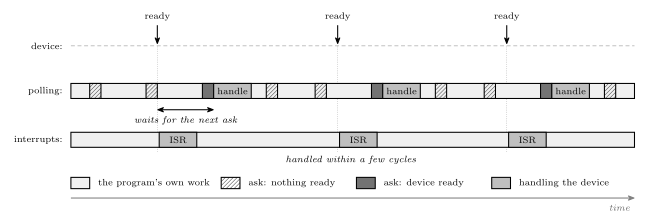
Figure 71: The same three device events handled both ways. Polling: the CPU breaks off its own work at fixed intervals to ask whether the device is ready. Most asks find nothing (hatched), and an event waits for the next ask before it is noticed, so how quickly it is handled depends on how often the program asks. Interrupts: the CPU does its work without asking, and each event diverts it into the handler within a few cycles. No time is spent asking, and the response does not depend on how long the main loop is. The work done is the same in both rows; what differs is the time wasted asking and the delay before each event is handled.
Interrupts are more efficient for the CPU, and they change the flow of control, which is where their cost lies.
A fourth way to leave the sequence
Normally the PC just increments. avr-branches-and-jumps and procedures-and-the-stack cover the instructions that change it. An interrupt changes it too, but without any instruction asking:
| Triggered by | Where the new PC comes from | Comes back? | |
|---|---|---|---|
| Branch | an instruction, if a flag says so | an offset in the instruction | no |
| Jump | an instruction | the instruction | no |
| Procedure call | an instruction (call) |
the instruction | yes: ret pops the return address call pushed |
| Interrupt | a device, between any two instructions | a table, indexed by which device | yes: the return-from-interrupt instruction pops the address the hardware pushed |
| Trap | an instruction that produces an exceptional result | a table, indexed by which error | not always |
The useful way to see an interrupt is as a procedure call that the hardware makes. The mechanism is the same: push the return address, load the PC, and pop it back at the end. The difference is that the program never asked for it, and that one difference produces all three of the issues below.
The three issues
Any interrupt mechanism has to answer three questions.
- How does the CPU know where the ISR is? A call names its target, but an interrupt does not, so the address must be found from the source. The CPU looks in an interrupt vector table, often at the beginning of memory. The table holds either the address of each handler, which the CPU loads into the PC, or a jump instruction to each handler, in which case the CPU loads the PC with the entry’s own address and executes the jump. The AVR does the second. Vector is used both for the interrupt’s number (its index in the table) and for the address of its handler, and it is worth checking which is meant.
- How are the registers preserved? All of them, including the status register. The handler must save copies of any register it uses before using it, and restore them before it returns. Many CPUs save the status register automatically; the AVR does not, so the handler must save it itself if it would change it. The result is transparency, below.
- What happens if another interrupt arrives while one is being serviced? Either it waits, or it interrupts the handler. See Nesting and priority, below.
The sequence of actions
From the device’s request to the resumed program there are fourteen steps, shared between the hardware and the ISR:
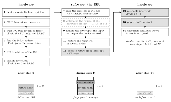
Figure 72: The fourteen steps of an interrupt, in the three phases the hardware and the ISR take turns at, with the state of the machine after each phase underneath. The hardware does the first six: it saves only the return address, finds and enters the handler, and turns interrupts off. The ISR saves what it will use, does the I/O and restores what it saved. The return-from-interrupt instruction then hands back to the hardware, which turns interrupts on and pops the return address. The notes in italics are the AVR’s version of each step. The shaded steps 11 to 13 are a single AVR instruction, reti, and step 8 rarely arises on the AVR (dashed), because every source has its own vector and so the ISR knows which one fired; only a pin-change handler, whose vector covers a whole port, still has to find which pin changed. The stack after step 14 is exactly as it was before step 1, and that is what transparency requires.
Three things in the sequence are worth holding on to:
- The hardware saves as little as it can. It pushes only the return address, and everything else is the ISR’s job. That keeps the entry fast, and it means an ISR that uses nothing need save nothing.
- Interrupts are off from step 6 to step 12. That is the default answer to issue 3: a second request simply waits until the handler has returned. On the AVR, off is the I bit of the status register being 0 (avr-architecture).
- Return from interrupt is not the same as return from procedure. It has to undo step 6 as well as step 3. A handler that ends with a plain
retgoes back to the right place but leaves interrupts disabled for good.
Transparency
When the ISR finishes, the computer is in the same state as it was before the interrupt. That is transparency, and it is the answer to issue 2. It matters more for an ISR than for a procedure because the interrupted code has no chance to prepare. A caller knows where its calls are and can agree with the procedure which registers it may use. An interrupt can land between any two instructions, including these two:
    cp   r16, r17        ; sets Z if r16 == r17
                         ; <- an interrupt here
    breq equal           ; reads Z
If the ISR does anything that sets flags — a dec, an andi, a cp of its own — and does not restore the status register, breq reads the ISR’s Z instead of the one cp produced. The program then takes the wrong branch, but only on the rare occasions the interrupt lands in that one gap. A bug like that can survive a great deal of testing. So the status register is the one register a handler must always consider, even if it touches nothing else. Whether an instruction changes it is listed per instruction in the instruction set reference (avr-instructions).
Nesting and priority
For an interrupt that arrives while an ISR is running, there are three policies:
- Disable interrupts during an ISR. The simplest: the second request waits (its flag stays set) and is serviced after the first handler returns. On CPUs that save the status register automatically, the global interrupt enable flag is among the bits the return-from-interrupt instruction restores, so it comes back on by itself. This is the AVR’s default.
- Prioritise. Higher-priority interrupts may interrupt lower-priority handlers, but not the other way round and not at the same level. Urgent devices are never kept waiting behind unimportant ones, and an unimportant device can never delay an urgent one. Many CPUs support this; the AVR does not.
- Re-enable interrupts inside the ISR. Any interrupt may then interrupt the handler, regardless of priority. The AVR allows this if the handler executes
sei.
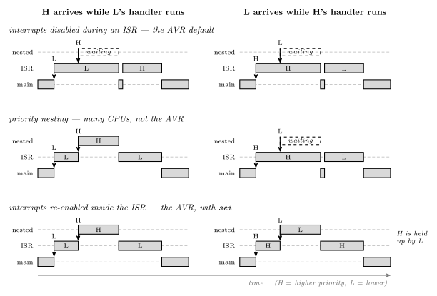
Figure 73: The three policies for an interrupt that arrives while another is being handled, in the two cases that tell them apart. In each panel, code on a higher lane has interrupted the code below it, and a dashed box is a request that is waiting. With interrupts disabled during an ISR, whichever handler started first finishes first, and the other waits for it in both cases. With priority nesting, the urgent request (H) cuts into the less urgent handler (L) but never the reverse, which is the behaviour one would want and the one the AVR does not provide. With interrupts re-enabled inside the handler, any request cuts in immediately, so in the right-hand case the urgent handler is itself held up by the less urgent one.
On the AVR, then, priority only decides the order in which waiting interrupts are serviced. It matters only when two or more are waiting at once, for instance because they arrived during another handler. The highest-priority one, the one with the lowest vector, goes first. It never lets an urgent interrupt cut into a running handler. The one way to get nesting is to re-enable interrupts inside the handler, and then priority plays no part at all. Both cases are traced, with the I bit, in 2026-09-21-interrupts.
The practical consequence is a rule: keep ISRs short. While any handler runs, every other interrupt waits. A handler that busy-waits for 10 ms delays every other device by 10 ms, and a timer tick that arrives twice during that time is serviced only once, because a flag can record that an event happened but not how many times.
Traps
Traps are software interrupts: interrupts caused by events in the software rather than in the hardware, and specifically by exceptional events, such as
- overflow,
- divide by zero, and
- an undefined opcode.
They relate to error checking the way interrupts relate to polling. Without traps, a program that must not overflow has to test after every arithmetic instruction, which is polling for errors. With them, the hardware watches, and the program is diverted only when the error actually happens. Traps save continually checking for errors.
Trap handlers don’t always return to the original program. After a division by zero or an undefined opcode, there is often no sensible instruction to continue with. Under an operating system the usual outcome is that the program is ended.
| Interrupt | Trap | |
|---|---|---|
| Caused by | a device, outside the program | the instruction being executed |
| When | at an unpredictable point in the program, asynchronously | at the same instruction every time, given the same data |
| Returns? | always, to the interrupted instruction’s successor | not always |
The AVR does not provide traps. Overflow sets V in the status register and it is up to the program to branch on it (avr-branches-and-jumps), and the AVR has no divide instruction to fail. But it is possible to generate hardware interrupts from software, by writing to an external interrupt pin configured as an output (avr-interrupts).
Pitfalls
- Assuming priority means pre-emption. On the AVR it does not: a higher-priority interrupt waits for a lower-priority handler to finish, like any other.
- Not saving the status register in a handler that changes flags. The symptom is an interrupted comparison going the wrong way, rarely and irreproducibly.
- Long handlers. Every other interrupt waits while one runs, and repeated events during the wait are merged into one.
- Variables shared between a handler and the main program that the compiler is allowed to cache. In C they must be
volatile(avr-interrupts). - Returning with
retinstead of the return-from-interrupt instruction: the program continues, and interrupts never come back on.
See also
- avr-interrupts — the ATmega324A’s vector table, ISRs in assembly and C, enabling an interrupt,
volatile, a complete timer-interrupt program - 2026-09-21-interrupts — Lecture 17, with the priority cases traced and worked questions
- procedures-and-the-stack —
call,retand the stack the return address goes on - avr-branches-and-jumps — the other ways the PC leaves its sequence
- avr-timers-and-counters — polling a timer flag, the thing interrupts replace
- software-timers — a tick interrupt as the program’s clock, and why busy waiting is the thing to avoid
- avr-usart · avr-spi · analog-to-digital-conversion — three devices that can be polled or left to interrupt
- fetch-decode-execute-cycle — the PC’s normal behaviour, increment and fetch
Procedures and the Stack
What a procedure is at the machine level, how call and ret get into it and back out, and the stack — the structure that makes returning possible from any depth of nesting, holds saved registers and arguments, and has to be set up before any of that works. First met in 2026-09-14-flow-of-control; branches and jumps are in avr-branches-and-jumps, and data memory, where the stack lives, is in memory-models and avr-architecture.
Procedures
A procedure is a group of instructions that performs some task, which
- may have operands — arguments or parameters,
- may produce result(s),
- can be invoked (called) from multiple places in a program — even from within itself, a recursive procedure — and
- after invocation, control returns to the statement after the call.
It is the same thing as a C function (c-language-basics), a Python function, a Java method, or a subroutine; the names differ by language, the mechanism does not. Good use of procedures is most of what makes a program of any size readable, and the AVR C compiler turns every function into exactly what follows.
The return is the part with machinery behind it. A jump goes somewhere; a call goes somewhere and remembers where it came from, so that a ret at the far end can come back — to a different place each time, depending on who called.
call and ret
| Instruction | Size | Cycles | |
|---|---|---|---|
call label |
direct call — target is an absolute address | 32-bit | 4 |
rcall label |
relative call — target is PC ± 2 K words | 16-bit | 3 |
icall |
indirect call — target is the address in Z | 16-bit | 3 |
ret |
return to the instruction after the most recent call | 16-bit | 4 |
The three calls mirror jmp, rjmp and ijmp exactly — same reach, same sizes — and each costs one cycle more than its jump. That cycle is the push. What a call does, in order:
- compute the return address — the address of the instruction after the call;
- push it onto the stack;
- load the PC with the target.
And ret undoes it: pop the top of the stack into the PC. Nothing in the procedure needs to know who called it, because the address to go back to was left on the stack by the caller.
Figure 74: A call and its return, followed through the three registers involved. The PC, the stack pointer and the top of the stack are shown before the call, during the procedure and after the return, with example addresses. call records the address of its own successor on the stack and lowers the stack pointer by two, because a program-memory address needs two bytes; then it loads the PC with the procedure’s address. ret reverses both steps and execution resumes at the recorded address, which is the instruction after the call. The procedure body never touches the return address, so it does not matter what the procedure does in between, provided it leaves the stack as it found it.
Why a stack
The return address has to be stored somewhere. There are three candidates:
| Where | Fails when |
|---|---|
| A single fixed register or memory address for all calls | a procedure calls another procedure — the second call overwrites the first’s return address, and the outer procedure can never return |
| One memory location per procedure | a procedure calls itself — recursion needs two live return addresses for one procedure |
| A stack | never, until memory runs out |
A stack is a last-in, first-out store: push puts a value on top, pop takes the top value off. Calls and returns nest — the most recent call is always the first to return — so a stack of return addresses always has the right one on top. Nested calls are drawn step by step in 2026-09-14-flow-of-control.
The AVR stack
On the AVR the stack is simply a region of data memory (memory-models), and the stack pointer is a 16-bit address held in two I/O registers, SPH:SPL, that says where the top currently is. Two conventions fix how it works:
- The stack grows downward. A push stores at the address in
SPand then decrementsSP; a pop incrementsSPand then loads from it. SoSPalways points at the next free cell, just below the most recently pushed byte. - It starts at the top of SRAM. Program variables are allocated from the bottom of SRAM upward; the stack is started at the last address,
RAMEND(0x08FFon the ATmega324A), and grows down toward them. Neither has to know in advance how much room the other needs.
Figure 75: Where the stack lives in the ATmega324A’s data memory. The general-purpose registers and I/O registers occupy the first 256 addresses; SRAM begins at 0x0100. Global variables are laid out from the bottom of SRAM upward, and the stack starts at the top, RAMEND, and grows downward toward them, with SPH:SPL holding the address of the next free cell. The gap between them is the free memory, and it shrinks from both ends: every nested call, every push and every local variable of a running function takes cells off the top, and the stack overflows when it reaches the variables — silently, since nothing checks. That is why the stack pointer must be set to RAMEND before the first call: the reset value would put it somewhere else entirely.
Initialising the stack pointer
An assembly program must initialise the stack before using it. These four lines belong at the top of RESET: in any program that calls anything:
.def temp=r16
    ldi  temp, low(RAMEND)
    out  SPL, temp
    ldi  temp, high(RAMEND)
    out  SPH, temp
RAMEND is defined by the device include file (avr-io-ports), and low()/high() split the 16-bit value because SPL and SPH are two separate 8-bit I/O registers. In C the compiler emits this itself as part of the start-up code that runs before main; it is one of the things a C program on the AVR gets for free and an assembly program does not. The RESET template in avr-program-structure does not include it only because nothing in the Lab 10 programs made a call.
push and pop
The two stack instructions are also available directly:
| Cycles | ||
|---|---|---|
push rr |
store rr at SP, then SP ← SP − 1 |
2 |
pop rd |
SP ← SP + 1, then load rd from SP |
2 |
Their main use is saving registers a procedure is about to clobber, so that the caller gets them back unchanged:
TEST:
    push r16           ; save what the caller had in r16 and r17
    push r17
    ...                ; use r16, r17 freely
    pop  r17           ; restore — in REVERSE order
    pop  r16
    ret
The order matters because the stack is LIFO: the last register pushed is the first one back. And the count matters even more — every push must be matched by a pop before the ret, because ret pops whatever is on top and treats it as the return address. One push too many and the procedure returns to an address made of a register’s contents; one too few and it returns into the middle of the saved data.

Figure 76: Saving and restoring registers around a procedure body, with the stack drawn after each instruction. The return address is already on the stack when the procedure starts; the two pushes go on top of it, and the two pops must come off in the reverse order to land in the right registers. When ret runs the return address is back on top, exactly as call left it. If the pops were in the same order as the pushes, r16 and r17 would come back swapped; if one pop were missing, ret would pop the saved r16 and jump to whatever address that byte pair happened to spell.
Arguments and results
Arguments are passed and results returned in one of two ways: in registers, or on the stack.
- Registers are the fast way for a few small values: the caller puts the argument in an agreed register before the
call, the procedure reads it there and leaves its result in an agreed register for the caller to pick up. Agreement is the whole trick — both sides must use the same register, and a procedure that uses registers for arguments cannot also expect them preserved. - The stack is the general way: the caller pushes the arguments, then calls; the procedure finds them on the stack just above the return address, and results can be returned the same way or in registers. The return address, the arguments and any saved registers and locals together are the procedure’s stack frame. It costs pushes and pops, but it works for any number of arguments and for recursion, since every live call has its own frame.
The AVR C compiler uses both: the first few arguments of a function travel in registers, r24 down, and the rest on the stack, and a function’s local variables live in its stack frame. Those details are the compiler’s convention, and they are why a C function call is not free — see the main costs in c-language-basics.
A C function’s stack frame
A C compiler puts a function’s local variables in its stack frame, next to the return address and any arguments passed on the stack. The frame is pushed when the function is called and popped when it returns. A local therefore exists only while its call is running, and each call, including each level of a recursion, gets its own copy at its own address. An optimising compiler keeps a small local in a register when it can. The frame is where it goes when it needs memory, and the lifetime is the same either way.
In address order, from high to low, which is the order they are pushed:
- arguments, pushed by the caller before the call, if any are passed on the stack;
- the return address, pushed by
call; - locals, made by the function itself when it starts.
A static local is not in the frame. It is stored with the globals, at a fixed address, so it outlives the call and still holds its value the next time the function runs. Globals sit at the bottom of SRAM, the heap grows up above them, and the stack grows down from RAMEND. A stack that grows far enough to meet the heap has overflowed. How the compiler lays out the whole data memory is in compilation-and-linking.
Figure 77: The stack frame of a C function while it runs, with the lowest address at the top as in the course’s memory maps. The caller pushed any stack arguments, call pushed the return address, and the function made room for its locals a and b above that. SP points at the next free cell, just above the frame. When the function returns, the whole frame is popped and SP goes back to where it was before the call, so a and b no longer exist. The static local c is not in the frame at all. It is stored among the globals at a fixed address, which is why it keeps its value from one call to the next.
The stack and interrupts
An interrupt uses the same stack in the same way. The hardware pushes the return address exactly as call would, and the handler’s reti pops it, like ret (avr-interrupts, 2026-09-21-interrupts). Three things follow:
- The stack pointer must be set before interrupts are enabled, not merely before the first
call. An assembly program with no procedures at all still needsSPinitialised once it uses an interrupt. - A handler’s pushes and pops must balance, and it must restore every register it uses. This is the same rule as for a procedure, but stricter: an interrupt can arrive between any two instructions, so there is no caller to agree anything with (polling-and-interrupts).
- Every interrupt that is being handled holds stack space: two bytes of return address plus whatever its handler pushes, and more again if handlers are allowed to nest.
Pitfalls
- Forgetting to initialise
SPin an assembly program. The firstcallpushes to wherever the reset value points; theretthen reads garbage. In C, not a concern. - Unbalanced push/pop inside a procedure — see Figure 76.
retdoes not check what it pops. - Stack overflow. Deep recursion, or big local arrays in C, walk the stack down into the heap and the variables. Nothing on the chip detects it; the symptom is variables changing value for no visible reason.
- Returning a pointer to a local. The local’s frame is popped by the return, so the pointer points at stack space that the next call will reuse.
- Clobbering the caller’s registers. A procedure that uses
r16without saving it changesr16for whoever called it. Either save and restore, or document which registers the procedure destroys — and be consistent.
See also
- avr-branches-and-jumps —
jmp,rjmp,ijmp, and the conditional branches - avr-program-structure — the
RESETtemplate the stack initialisation goes into - memory-models · avr-architecture — data memory,
RAMEND, and the I/O registersSPH/SPL - avr-instructions —
push,pop,call,retamong the rest - c-language-basics — functions in C, which compile to exactly this
- compilation-and-linking — where the compiler puts globals, locals, statics and the heap · 2026-10-15-compilation-and-linking — Lecture 22
- avr-interrupts · polling-and-interrupts — the same stack, used by the hardware
- 2026-09-14-flow-of-control — Lecture 15 · 2026-09-21-interrupts — Lecture 17, the stack under interrupts
Serial Communication
Sending data between devices one bit at a time, and how the receiving end makes sense of what arrives: serial against parallel, synchronous against asynchronous, the UART frame, parity, how a receiver samples the line, and baud rate. Then the synchronous serial buses, where one master clocks data to and from several slaves: SPI and I²C, compared with the UART, and bit bashing for when there is no hardware for a standard. The AVR’s hardware is in avr-usart and avr-spi. First met in 2026-09-24-serial-io and 2026-10-05-more-io.
Serial and parallel
| Parallel | Serial | |
|---|---|---|
| Wires carrying data | one per bit | one |
| How a byte travels | all 8 bits at once | 8 bits one after another |
| Cost | many pins and wires | time: a byte takes 8 bit times |
Inside a chip, data moves in parallel: a port is eight pins, a register is eight flip-flops. Between devices, pins and wires are what is scarce, so nearly every link is serial. The conversion at each end is the job of a shift register (shift-registers): load a byte in parallel and shift it out one bit at a time to send, shift bits in and read the byte out in parallel to receive.
By convention the sending end of a link is Tx and the receiving end is Rx. A device that does both has one of each, and two such devices are joined crossed over: each one’s Tx goes to the other’s Rx.
Synchronous and asynchronous
A receiver has to know when to look at the data wire, as well as what is on it. There are two ways to tell it.
Synchronous: one end sends a clock on a second wire. The receiver reads the data wire on each clock edge. Nothing has to be agreed in advance about speed, beyond the fastest the receiver can follow. SPI, the Serial Peripheral Interface, and I²C both work this way (below).
Asynchronous: there is no clock wire. Each end has its own clock, the two agree on the speed beforehand, and the receiver recovers the exact timing from the data stream itself. That only works if the stream is guaranteed to contain edges to time against, so the data is encoded:
| Encoding | How it guarantees edges | Used by |
|---|---|---|
| start and stop bits | every character begins with a fall from 1 to 0 | UART |
| 4B/5B, 8B/10B | every 4 or 8 bits are replaced by a 5- or 10-bit code that never has a long run | fast network links |
| bit stuffing | an opposite bit is inserted after a run of identical bits | USB at low and full speed |
A UART is a Universal Asynchronous Receiver and Transmitter. A USART can also work synchronously. The pictures of all four cases are in 2026-09-24-serial-io.
The UART frame
A UART sends data in frames. Between frames the line rests at 1, the idle level. A frame is:
| Order | Field | How many | Value |
|---|---|---|---|
| 1 | start bit | 1 | always 0 |
| 2 | data bits | 5 to 9 | the data, least significant bit first |
| 3 | parity bit | 0 or 1 | chosen to make the count of 1s even or odd |
| 4 | stop bits | 1 or 2 | always 1 |
Why each part is there:
- The start bit is 0 because the idle line is 1. The fall from 1 to 0 is the one event the receiver can be sure of, and everything else is timed from it.
- The stop bit is 1 so that the line is back at the idle level when the frame ends. Whatever the last data bit was, the next start bit is then a fall again.
- The data bits go least significant first. A receiver that assumes the opposite reads every byte bit-reversed.
The format is usually written as three items: data bits, parity (N for none, E for even, O for odd), stop bits. 8N1 is 8 data bits, no parity, 1 stop bit, and is by far the commonest.
Worked: the letter s
A character is sent as its ASCII code (c-language-basics). The letter s is 115, 0x73, 0111 0011. In 8N1 the line carries, in time order:
| start | b0 | b1 | b2 | b3 | b4 | b5 | b6 | b7 | stop |
|---|---|---|---|---|---|---|---|---|---|
| 0 | 1 | 1 | 0 | 0 | 1 | 1 | 1 | 0 | 1 |
Read left to right, the data bits are 1100 1110, the byte written backwards.
Figure 78: The letter s, 0x73, on the wire as an 8N1 frame. Time runs left to right and each cell is one bit time. The line idles at 1, falls for the start bit, carries the eight data bits least significant first, and returns to 1 for the stop bit. Written most significant bit first the byte is 0111 0011; the wire carries it in the opposite order.
Parity
The parity bit lets the receiver detect that a frame was damaged. The two ends agree on the kind:
- Even parity: the number of 1s in the data bits and the parity bit together is even.
- Odd parity: that number is odd.
To send: count the 1s in the data. Choose the parity bit that makes the total the agreed kind.
To check: count the 1s in the data and the parity bit as received. If the total is the wrong kind, there was an error.
| Data | 1s in the data | Even parity bit | Odd parity bit |
|---|---|---|---|
0xA7 = 1010 0111 |
5 | 1 | 0 |
0xA9 = 1010 1001 |
4 | 0 | 1 |
0x73 = 0111 0011 |
5 | 1 | 0 |
0x00 = 0000 0000 |
0 | 0 | 1 |
The even parity bit is the XOR of the data bits (logic-gates): XOR is 1 exactly when an odd number of its inputs are 1, which is exactly when a 1 is needed to make the total even. The odd parity bit is its complement.
Worked check. 0xA9 arrives with parity bit 1 on an even-parity link. The data has four 1s, and the parity bit makes five. Five is odd, so the frame is in error.
What parity cannot do:
- It cannot say which bit is wrong, so it cannot correct anything. The frame has to be discarded or sent again.
- It misses any even number of flipped bits. Two flips cancel and the count comes out right.
Detecting and correcting needs several check bits arranged so that the pattern of failed checks points at the wrong bit. That is a Hamming code, and it is not part of a UART frame.
Sampling: finding the bits without a clock
The receiver knows the bit time from the agreed baud rate. What it does not know is when a frame will start. It finds out by watching:
- It samples the line many times per bit: 16 on the AVR.
- While the line is idle, every sample is 1. A sample of 0 means a start bit may have begun, and the receiver starts counting samples from there.
- It reads the three samples at the centre of each bit time and takes the majority. For the first bit time the answer must be 0, or the fall was only noise and the receiver goes back to waiting.
- It carries on, one bit time after another, for the data bits, the parity bit if there is one, and the stop bit.
- The stop bit must read 1. If it reads 0 the frame is wrong: a framing error, usually a sign that the two ends disagree about the baud rate or the format.
The picture is in 2026-09-24-serial-io.
Why the clocks need not match exactly. Suppose the receiver’s clock is slightly slow. Each sampling point is then a little later within its bit than the one before, and by the last bit of the frame the lateness has added up. As long as the total stays under half a bit time, every sample still lands inside the right bit. A 10-symbol frame gives the error about ten bit times to build up, so the two clocks have to agree to within a few percent. At the next start bit the count starts again from the new falling edge and the accumulated error is gone. That re-timing on every frame is what the start bit is for.
Baud rate and bit rate
Baud rate = symbols per second. Bit rate = useful data bits per second.
On a UART line a symbol is one bit time, and start, parity and stop bits are symbols that carry no data. So the bit rate is always lower than the baud rate, by the fraction of the frame that is data.
| Format | Symbols per frame | Data bits | Data fraction | At 9600 baud |
|---|---|---|---|---|
| 8N1 | 10 | 8 | 80 % | 7680 bit/s, 960 bytes/s |
| 8E1 or 8O1 | 11 | 8 | 73 % | 6982 bit/s, 873 bytes/s |
| 8N2 | 11 | 8 | 73 % | 6982 bit/s, 873 bytes/s |
| 7E1 | 10 | 7 | 70 % | 6720 bit/s, 960 characters/s |
The method: frames per second is the baud rate divided by the symbols per frame, and bits per second is that times the data bits per frame. For 8N1 at 9600 baud, \(9600 / 10 = 960\) frames per second and \(960 \times 8 = 7680\) bits per second.
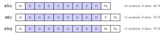
Figure 79: Three frame formats, one cell per symbol. Shaded cells carry data and white cells are framing. Every format here carries eight data bits, so adding a parity bit or a second stop bit makes the frame eleven symbols long instead of ten, and at the same baud rate fewer frames fit into a second.
The standard baud rates are 2400, 4800, 9600, 14400, 19200, 28800, 38400, 57600 and 115200.
Both ends must agree
Four settings define a UART link, and none of them is sent over it:
- the baud rate;
- the number of data bits;
- the parity: none, even or odd;
- the number of stop bits.
A terminal program on a PC asks for all four, plus which serial port to use. If the two ends differ, the receiver still samples the line and still produces bytes. They are just the wrong bytes, sometimes with framing or parity errors flagged and sometimes not. Garbled characters on a terminal almost always mean a mismatch here, most often the baud rate.
RS232
A serial standard more than 40 years old and still in use, typically on a 9-pin D-sub connector. Its frames are UART frames. Its voltages are not the microcontroller’s:
| Microcontroller pin | RS232 line | |
|---|---|---|
| logical 1 | 5 V | negative, −3 V to −15 V |
| logical 0 | 0 V | positive, +3 V to +15 V |
So RS232 is inverted and uses larger voltages of both signs. A level-converter chip such as the MAX-232 goes between an AVR pin and an RS232 line. Connecting the two directly does not work and can damage the pin.
RS232 is full duplex: there is a separate wire for each direction, so both ends can transmit at once. The standard defines many signals, and the smallest useful set is three: TxD, RxD and ground. Ground is needed because a voltage only has meaning against a reference both ends share.
Buses: masters and slaves
A UART joins exactly two devices. A bus is a set of wires shared by several, and that raises the question of who decides when a transfer happens.
- The master initiates and controls the transfer of data: it decides when a transfer starts, which device it is with and which way the data goes, and on a synchronous bus it drives the clock.
- A slave waits for requests and responds to the master. It never starts a transfer.
Some devices can be both, at different times. The AVR’s SPI and TWI ports can each be set up as a master or as a slave, and on an I²C bus more than one device may take a turn at being master. Memory can never be a bus master: all a memory can do is answer a read or a write of an address that something else has chosen. On a processor’s memory bus the CPU is the master.
Synchronous serial buses
Both buses here send a clock from the master alongside the data, so neither needs start and stop bits or an agreed baud rate. They differ in how the master picks which slave it is talking to.
SPI
The Serial Peripheral Interface has four signals: the clock SCK, a data wire each way, MOSI (master out, slave in) and MISO (master in, slave out), and an active-low select \(\overline{\text{SS}}\) for each slave. The master and the slave each hold an 8-bit shift register, and MOSI and MISO join them into a ring, so on every clock pulse one bit goes each way. Eight pulses swap the two bytes: every transfer is an exchange. Several slaves either get a select line each, or are daisy-chained on one select with the data passing through each in turn. All of this, with the AVR’s SPI port, is in avr-spi.
I²C and TWI
I²C, the Inter-Integrated Circuit bus, was created by Philips Semiconductor, now NXP. TWI, the Two-wire Interface, is Atmel’s name for it. There are two wires, and every device connects to both:
- SDA, serial data, which carries data in either direction, one way at a time;
- SCL, serial clock, driven by the master.
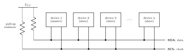
Figure 80: An I²C bus. Every device connects to the same two wires: SDA carries the data, in either direction, and SCL carries the clock from the master. No device ever drives a line high. Each can only pull a line low or let go of it, and the two pull-up resistors hold a line at 1 while nobody is pulling, so two devices can never fight over a line. Because every device hears every transfer, the master begins each one with the address of the slave it is for. A dot is a connection; where a lead crosses SDA without a dot there is no connection.
Why the pull-ups. Every output on the bus is open drain: it can connect its line to ground or leave it alone, and never connects it to \(V_{CC}\). A line is 1 when nobody is pulling it down and 0 when anybody is. Any number of devices can share a wire that way without two outputs ever fighting.
Addresses instead of select lines. Every device sees every transfer, so the master starts each one by sending the address of the slave it wants, and only that slave answers. Adding a device adds no wires.
On the ATmega324A the TWI uses PC0 as SCL and PC1 as SDA, and the datasheet describes it on pages 211 to 239 (2026-10-05-more-io).
UART, SPI and I²C compared
| UART | SPI | I²C / TWI | |
|---|---|---|---|
| Clock | none: both ends agree a baud rate | SCK, from the master | SCL, from the master |
| Data wires | TxD and RxD, one each way | MOSI and MISO, one each way | SDA, shared by both directions |
| Both directions at once? | yes | yes: every transfer is an exchange | no |
| Devices | two | one master, many slaves | many, some able to be master |
| Choosing a slave | no need: only two ends | a select line per slave, or a daisy chain | an address sent on the bus |
| Wires, besides ground | 2 | 3, plus a select per slave | 2 |
| On the ATmega324A | USART0 (PD0, PD1), USART1 (PD2, PD3) | one SPI port, PB4 to PB7 | one TWI port, PC0 and PC1 |
Bit bashing
Sometimes a microcontroller has no hardware support for a bus standard, or not enough interfaces of it. The standard can still be used by simulating it on general purpose port pins: the program sets and clears the output pins and reads the input pins itself, in exactly the order the standard lays down. That is bit bashing, also called bit banging.
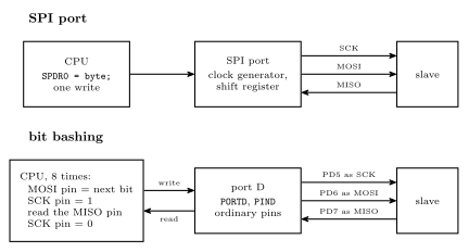
Figure 81: Who does the work. Above, with an SPI port: the program writes one byte to the data register and the port’s own clock generator and shift register produce all eight clock pulses and move all sixteen bits, while the CPU is free. Below, bit bashing the same transfer on three ordinary pins of port D: the CPU runs a loop that puts each bit on the MOSI pin, raises and lowers the SCK pin and reads the MISO pin, eight times over, through the port’s PORTD and PIND registers. The slave cannot tell the difference. The CPU is busy for the whole transfer, and the clock can go no faster than the loop.
Worked: an SPI master in software
Three spare pins of port D, plus one for the select, can be an SPI master in mode 0, most significant bit first, with nothing but the set, clear and test idioms of bit-masking:
#define BB_SS    4                 /* port D pins used for the software SPI */
#define BB_SCK   5
#define BB_MOSI  6
#define BB_MISO  7

void bb_init(void) {
    DDRD  |= (1<<BB_SS) | (1<<BB_SCK) | (1<<BB_MOSI);   /* outputs; MISO stays an input */
    PORTD |= (1<<BB_SS);                                /* nothing selected             */
    PORTD &= ~(1<<BB_SCK);                              /* the clock rests low          */
}

uint8_t bb_exchange(uint8_t out) {
    uint8_t in = 0;
    uint8_t i;

    for (i = 0; i < 8; i++) {
        if (out & 0x80) {                    /* put the top bit on MOSI           */
            PORTD |= (1<<BB_MOSI);
        } else {
            PORTD &= ~(1<<BB_MOSI);
        }
        out <<= 1;
        PORTD |= (1<<BB_SCK);                /* rising edge: both ends read       */
        in = (in << 1) | ((PIND >> BB_MISO) & 1);
        PORTD &= ~(1<<BB_SCK);               /* falling edge: the slave moves on  */
    }
    return in;
}
Used like the hardware version: pull BB_SS low, call bb_exchange once per byte, raise BB_SS. Reading MISO straight after raising SCK is safe, because the slave put that bit out on the previous falling edge, or when it was selected, and it stays put until the next falling edge.
What it costs.
- The CPU does everything. Each bit is several instructions, so the clock runs far slower than the 4 MHz the SPI port can make, and the program does nothing else meanwhile.
- Synchronous standards bash easily. The master makes the clock, so if the loop is held up between two edges, by an interrupt for instance, the transfer simply pauses. The slave waits for the next edge however long it takes.
- Asynchronous standards are harder. A bit-bashed UART has no clock to wait for, so every bit time has to be produced exactly, and an interrupt landing in the middle of a frame can wreck it.
Common mistakes
- Tx to Tx. The link is crossed: one end’s transmit pin goes to the other’s receive pin.
- Treating baud rate as bit rate. 9600 baud in 8N1 moves 7680 data bits a second, not 9600.
- Reading the bits most significant first. A UART sends bit 0 first.
- Leaving the parity bit out of the count. The rule is about the data bits and the parity bit together.
- Expecting parity to fix or locate an error, or to catch every error.
- Drawing the idle line at 0. Idle is 1, the start bit is 0, the stop bit is 1.
- Forgetting ground between two boards.
- Crossing SPI’s data wires. MOSI goes to MOSI and MISO to MISO: the names already say which end drives.
- Leaving out the pull-ups on an I²C bus. Nothing ever drives the lines high, so without them they never return to 1.
- Thinking memory could start a transfer. Memory is always a slave.
See also
- avr-usart — the ATmega324A’s USART: registers, baud-rate values, code and interrupts
- avr-spi — the ATmega324A’s SPI port: the exchange, timing, several slaves, registers, clock rate, code
- bit-masking — the set, clear and test idioms the bit-bashing code is made of
- shift-registers — parallel in, serial out, and the reverse
- logic-gates — XOR, which computes a parity bit
- timing-diagrams — how the waveforms here are drawn and read
- magnetic-disks — a disk sector, framed like a UART frame: preamble, data, ECC, gap
- io-board — the USB-serial device that joins the breadboard to a PC
- 2026-09-24-serial-io — Lecture 18 · 2026-10-05-more-io — Lecture 19
Shift Registers
Registers and shift registers are the simplest useful sequential circuits — groups of D flip-flops sharing a common clock.
Registers
- A register is a group of flip-flops. An \(n\)-bit register consists of \(n\) flip-flops and is capable of storing \(n\) bits.
- A register is a sequential circuit without any combinational logic — it is just the storage elements and their shared control lines.
- Registers are used to store binary information (data/instructions) inside a processor.
A 4-bit register:
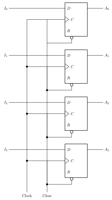
Figure 82: A 4-bit register (Mano, Digital Design, 3rd ed.). Four flip-flops, four parallel inputs, four parallel outputs, and exactly two shared control lines — no gate anywhere, which is what makes a register a sequential circuit without combinational logic. The pin labelling is Mano’s, which differs from the rest of the course: the clock input is lettered C rather than CLK and the asynchronous clear is lettered R, marked active-low by the bubble on the pin. The course uses several labellings for both (see the diagram-notation note).
| Signal | Connection |
|---|---|
| \(I_0 \ldots I_3\) | the four parallel data inputs, one to each flip-flop’s \(D\) input |
| \(A_0 \ldots A_3\) | the four parallel outputs, taken from each flip-flop’s \(Q\) |
Clock |
a single common line driven to the \(C\) (clock) input of all four flip-flops |
Clear |
a single common line driven to the \(R\) (reset) input of all four flip-flops, drawn active-low (bubble on the input) |
So on each rising clock edge all four flip-flops simultaneously capture their \(I\) inputs; asserting Clear forces all four outputs to 0 asynchronously (see flip-flops-and-latches for asynchronous SET/CLR).
Shift registers
A shift register is a register which is capable of shifting its binary information in one or both directions.
The 4-bit shift register example is built as a chain: the serial input \(SI\) feeds the \(D\) input of the first flip-flop; each flip-flop’s \(Q\) output feeds the next flip-flop’s \(D\) input; the last flip-flop’s \(Q\) is the serial output \(SO\). All four flip-flops share a common \(CLK\) line.
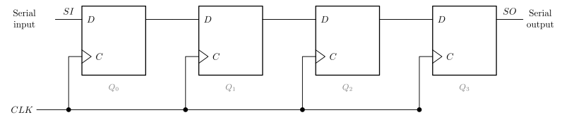
Figure 83: The 4-bit shift register (Mano’s Fig. 6-3). The whole device is four D flip-flops and one wire each: the only structural difference from the register above is where each D input comes from. The grey stage names Q0 to Q3 are there so the trace table below can be read against the drawing.
On each rising clock edge every stored bit moves one place along the chain, the bit currently on \(SI\) enters the first stage, and the bit that was in the last stage leaves at \(SO\).
The common clock is what makes the shift well-defined. Every flip-flop samples its \(D\) input at the same instant, so each stage captures its neighbour’s old value, not the new one the neighbour is simultaneously taking on; the whole word moves exactly one place per edge rather than racing along the chain. This is the point of the rule that in a synchronous sequential circuit all the sequential elements share a common clock signal — see sequential-circuits.
Worked through by hand, with stages labelled \(Q_0\) (nearest \(SI\)) through \(Q_3\) (= \(SO\)), starting from all zeros and shifting in the bit sequence 1, 0, 1, 1:
| Clock edge | \(SI\) | \(Q_0\) | \(Q_1\) | \(Q_2\) | \(Q_3\) (\(=SO\)) |
|---|---|---|---|---|---|
| (initial) | — | 0 | 0 | 0 | 0 |
| 1 | 1 | 1 | 0 | 0 | 0 |
| 2 | 0 | 0 | 1 | 0 | 0 |
| 3 | 1 | 1 | 0 | 1 | 0 |
| 4 | 1 | 1 | 1 | 0 | 1 |
After 4 clock edges the 4 serially-supplied bits sit in the 4 flip-flops, and one further edge would push the first of them out of \(SO\).
Serial ↔︎ parallel conversion
Shift registers can be used to do serial-to-parallel conversion, and vice versa. This is the reason they show up everywhere data has to travel over a single wire but be used a word at a time.
- Serial in, parallel out: drive the bits one per clock edge into \(SI\); after \(n\) edges, the \(n\) flip-flop \(Q\) outputs — read as a group — are the parallel word. This is exactly the table above: clock 4 bits in, then read \(Q_0 Q_1 Q_2 Q_3\) in parallel.
- Parallel in, serial out: load the \(n\) bits into the flip-flops in one clock edge (a parallel load — see Figure 84), then read them off \(SO\) one bit per edge — the first bit is sitting at \(SO\) as soon as the load edge lands, and \(n-1\) further edges bring the rest.
The parallel outputs are simply the \(Q\) pins of the flip-flops already present in Figure 83, brought out as a group. Nothing extra is added to the circuit for serial-in/parallel-out at all.
Parallel load vs serial shift
A plain shift register can only be filled one bit per clock. To also allow parallel load — all \(n\) bits written at once from \(n\) parallel inputs — each flip-flop’s \(D\) input is fed from a 2-to-1 multiplexer (see combinational-logic-blocks) instead of directly from the previous stage:
| Mux select | Mux data input chosen | Effect on that stage |
|---|---|---|
| “shift” | the previous stage’s \(Q\) (or \(SI\) for the first stage) | serial shift by one place |
| “load” | that stage’s parallel data input \(I_i\) | parallel load of the whole word in one clock edge |
The select line is common to all the muxes, so on each clock edge the register either shifts by one place or loads the whole parallel word.
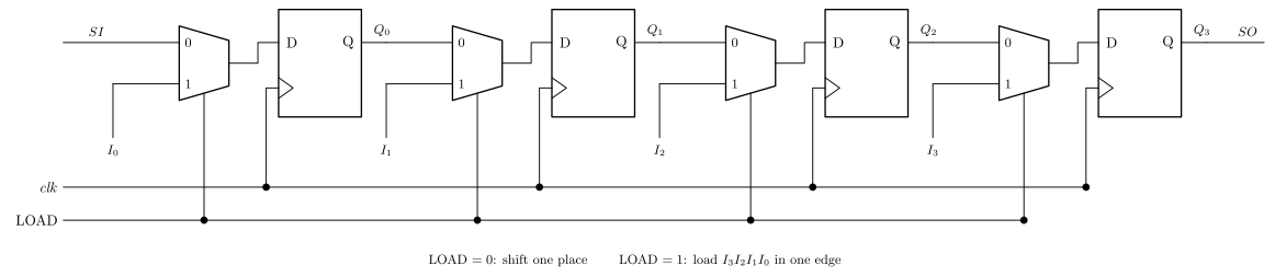
Figure 84: The parallel-load shift register: one 2-to-1 multiplexer in front of every flip-flop’s D input, with a single LOAD line steering all four at once. Follow the top mux input across and it is the plain chain of the previous figure; follow the bottom input and every stage is loaded from its own I pin in one edge. The Q pins do double duty as the parallel output. Which mux input is which is a free choice: here LOAD equals 0 for shift and 1 for load.
Adding a hold. The same trick gives a register an enable: widen each mux by one input and wire that input to the stage’s own \(Q\), so on a “hold” edge every flip-flop reloads the value it already has and the word does not move. This is the standard way to stop a register without gating the clock — gating the clock risks glitching it — and it is what a “recirculating” input means. It follows from the mux construction, and a past-paper question turns on it (csse2010-sample-midsem-1 Q18, where each mux’s input 0 is its own stage’s \(Q\) looped back, so the control line chooses shift or hold).
The mux-based bidirectional shift element
A single building block makes a shift register that shifts in either direction (drawn in the lecture note):
- a 2-to-1 multiplexer whose output drives the \(D\) input of one D flip-flop;
- the mux’s select line is a control signal called DIRN;
- DIRN = 0 selects mux input 0 → left shift;
- DIRN = 1 selects mux input 1 → right shift;
- the flip-flop’s \(Q\) is that stage’s output, and the flip-flop is clocked from the common clock.
Chaining \(n\) of these elements and wiring, for each stage, mux input 0 to the neighbour on the left-shift side and mux input 1 to the neighbour on the right-shift side gives an \(n\)-bit bidirectional shift register: one shared DIRN line decides which way the whole register shifts on the next clock edge.
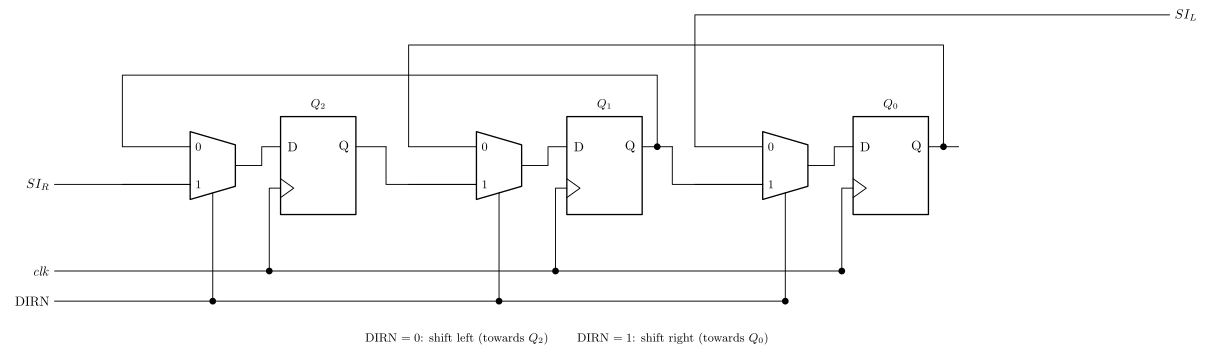
Figure 85: A 3-bit bidirectional shift register: three copies of the DIRN element, one shared DIRN line and one shared clock. Q2 is the most significant bit, on the left. Mux input 0 of every stage comes from the stage on its right (left shift, bits moving towards Q2); mux input 1 comes from the stage on its left (right shift). The two ends need a serial input each, because on each direction one end has no neighbour to take a bit from. Wires that cross without a dot are not connected.
For a 3-bit register with bits \(Q_2 Q_1 Q_0\) (\(Q_2\) most significant), taking left shift to mean bits move towards the more-significant end:
| Stage | Mux input 0 (DIRN=0, left shift) | Mux input 1 (DIRN=1, right shift) |
|---|---|---|
| \(Q_2\) | \(Q_1\) | \(SI_R\) (serial input for right shifts) |
| \(Q_1\) | \(Q_0\) | \(Q_2\) |
| \(Q_0\) | \(SI_L\) (serial input for left shifts) | \(Q_1\) |
One clock edge applied to a 3-bit register holding \(Q_2 Q_1 Q_0 = 110\), with both serial inputs held at 0:
| DIRN | Operation | Before (\(Q_2Q_1Q_0\)) | After (\(Q_2Q_1Q_0\)) |
|---|---|---|---|
| 0 | left shift | 110 | 100 |
| 1 | right shift | 110 | 011 |
See 2026-08-13-shift-registers for the exercise that asks for this register.
The configurations a shift register can be wired into
There are seven named configurations, parts (a) to (g) of a figure from Floyd, recapped at the start of Lecture 7:
- serial in / shift right / serial out
- serial in / shift left / serial out
- parallel in / serial out
- serial in / parallel out
- parallel in / parallel out
- rotate right
- rotate left
The first six are all the same flip-flop chain differing only in where each \(D\) comes from and which pins are brought out: adding a mux per stage buys the parallel input, tapping the \(Q\) pins buys the parallel output, and swapping the direction of the chain buys left instead of right. The last two, the rotates, are the chain with its serial output wired back to its serial input, so no bit is lost and the word cycles.
Universal shift register
A universal shift register is the combination of all of the above capabilities in one device: it can hold its value, shift left, shift right, and be parallel-loaded, with the operation selected by control inputs.
Structurally it is the two constructions above stacked: four operations need a 4-to-1 mux per flip-flop and two select lines, with the four mux inputs being the stage’s own \(Q\) (hold), its left neighbour, its right neighbour, and its parallel input \(I_i\).
Wide (multi-bit) shift registers
A shift register does not have to shift one bit at a time — it can shift a whole multi-bit word per clock edge. An example is an 8-bit wide, 4-stage queue:
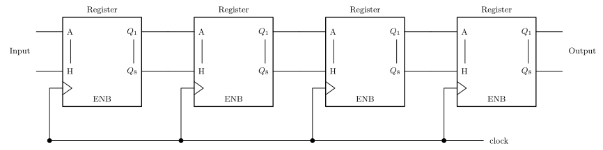
Figure 86: The 4-stage 8-bit queue. Each block is a whole 8-bit register rather than a single flip-flop: the vertical line between A and H, and between Q1 and Q8, is shorthand for the six pins in between. Functionally identical to the 1-bit chain — one stage’s outputs are the next stage’s inputs, everything on one clock — but each stage now holds a byte, so a byte presented at Input reaches Output four clock edges later.
- four registers in a row, each 8 bits wide (inputs labelled \(A\) through \(H\), outputs labelled \(Q_1\) through \(Q_8\));
- the 8-bit
Inputbus feeds the first register’s 8 data inputs; - each register’s 8 \(Q\) outputs feed the next register’s 8 data inputs, as a bus;
- the last register’s outputs are the 8-bit
Output; - all four registers share a common clock line, and each has an
ENB(enable) input.
Functionally this is the same chain as the 1-bit shift register, but each “stage” holds a byte rather than a bit — so it behaves as a 4-deep queue of bytes: a byte presented at Input appears at Output four clock edges later.
This is also the shape the Lab 06 combination lock takes, at a smaller size: a two-stage, 4-bit-wide shift register, so that each press of the “enter” button moves a whole digit from the first stage to the second. See the lecture note and week4-lab-sequential-circuits-shift-registers.
Comments and directives
Comments start with semicolons. Everything from a
;to the end of the line is ignored by the assembler..include "m324Adef.inc"is an assembler directive, not an instruction — nothing is generated for it. The contents of the file are included directly in the program, which is what makesDDRA,PORTC,TCNT0and the rest usable as names instead of I/O register numbers (see avr-io-ports). The leading dot is the giveaway: a line starting.speaks to the assembler, a line starting with a mnemonic speaks to the CPU.Every line has the same shape, with up to four fields: a label, an operation, its operands and a comment, as in
loop: jmp loop ; Repeat. The operation is either an instruction or, with the leading dot, a directive. Two more directives turn up in most programs:.def temp = r16gives a register a name, and.equgives a number a name. The fields, and every directive with what it does, are in assembly-process.