Sample Mid-semester Exam #1
exercises
exam
past-paper
computer-systems
This is the first of UQ’s sample mid-semester papers for csse2010 — CSSE2010/CSSE7201 Introduction to Computer Systems — printed for the Semester One Mid-semester Examinations, 2020, St Lucia campus. It runs for 60 minutes with 10 minutes of reading time beforehand, and it is an open book examination: no electronic aids (laptops, phones), but a Casio FX82-series or other UQ-approved calculator is allowed. Answers go on a supplied “True/False and Multiple Choice Answer Sheet”. There are 25 questions, each worth one mark, and the marking is blunt — a correct answer earns one mark, and an incorrect, missing or multiple answer earns zero, so there is no penalty for guessing.
WarningAnswers are derived, not official
The source paper ships without an answer key, so every answer below was worked out during transcription rather than taken from UQ. Each one shows its reasoning so it can be checked rather than trusted; anything uncertain is flagged. Treat a disagreement between your working and the answer here as a reason to check both.
How to use this
Two ways. For a timed run, set a clock for 60 minutes and work straight through all 25 questions — on the website the answers are collapsed, so they stay hidden until you click them, and the paper reads like the real thing. For targeted practice, use the question index below to pick out only the questions for one week or one concept, and follow the concept links when a step in the working is unfamiliar. Note that the PDF build prints every answer inline, so the site version is the one to practise from.
Question index
| Q | Topic | Week | Concept notes |
|---|---|---|---|
| 1 | One’s complement | 1 | binary-number-representations |
| 2 | Octal conversion | 1 | binary-number-representations |
| 3 | Range of a radix-r number | 1 | binary-number-representations |
| 4 | Properties across signed formats | 1 | binary-number-representations |
| 5 | Reading a gate-level circuit | 1 | logic-gates |
| 6 | Gate equivalence and De Morgan | 1 | logic-gates · boolean-algebra |
| 7 | Boolean simplification | 2 | boolean-algebra |
| 8 | Truth table to sum of products | 2 | boolean-algebra |
| 9 | Timing diagram to logic function | 2 | timing-diagrams |
| 10 | XOR identities | 2 | boolean-algebra |
| 11 | NOR-only implementation | 2 | boolean-algebra · logic-gates |
| 12 | NOR latch behaviour | 3 | flip-flops-and-latches |
| 13 | D flip-flop timing | 3 | flip-flops-and-latches · timing-diagrams |
| 14 | Two’s complement addition | 2 | binary-number-representations |
| 15 | Detecting overflow | 2 | binary-number-representations |
| 16 | Overflow on a positive sum | 2 | binary-number-representations |
| 17 | Programming a multiplexer | 2 | combinational-logic-blocks |
| 18 | Shift register with hold | 3 | shift-registers |
| 19 | Counter width | 4 | counters |
| 20 | Synchronous counter sequence | 4 | counters |
| 21 | State diagram to state table | 4 | state-machines |
| 22 | Tracing a state machine | 4 | state-machines |
| 23 | Tanenbaum ALU bit slice | 5 | arithmetic-logic-unit |
| 24 | ALU bit slice with an 8-way mux | 5 | arithmetic-logic-unit |
| 25 | What an ALU cannot compute | 5 | arithmetic-logic-unit |
Q1 — One’s complement of a negative
What is \(-21_{10}\) expressed in 8-bit one’s complement format?
10010101
11101010
11101011
11110010
None of the above
TipAnswer
(b)
One’s complement negates by inverting every bit of the magnitude, so start from \(+21\) in 8 bits:
\[21 = 16 + 4 + 1 = 0001\,0101_2\]
Inverting all eight bits gives
\[\overline{0001\,0101} = 1110\,1010_2\]
which is option (b). Option (c), 11101011, is the two’s complement of \(-21\) (one’s complement plus one) — the classic distractor here. See binary-number-representations.
Q2 — Octal conversion
\(111_8\) is equal to
\(1001001_2\)
\(71_{10}\)
0x73
\(7_{10}\)
None of the above
TipAnswer
(a)
Each octal digit is exactly three bits, so the conversion to binary is done digit by digit with no arithmetic at all:
\[1_8 \to 001, \quad 1_8 \to 001, \quad 1_8 \to 001 \;\Rightarrow\; 111_8 = 001\,001\,001_2 = 1001001_2\]
That is option (a). Checking the others against the decimal value \(1 \times 64 + 1 \times 8 + 1 = 73_{10}\): (b) is 71, not 73; (d) is 7; and (c) is the trap — 0x73 is hexadecimal 73, which is \(7 \times 16 + 3 = 115_{10}\), not the decimal 73 the value happens to equal. See binary-number-representations.
Q3 — Range of a radix-r number
An n-digit radix-r number can represent unsigned integer values from 0 up to
\(2^{(n-1)}\)
\(2^n\) - 1
\(r^{(n-1)}\) - 1
\(r^n\) - 1
None of the above
TipAnswer
(d)
With \(n\) digits and \(r\) choices per digit there are \(r^n\) distinct patterns. Counting from zero, the largest value is one less than the count:
\[0 \le \text{value} \le r^n - 1\]
Two other routes to the same answer:
- The smallest value you cannot represent is a one followed by \(n\) zeroes, which is worth \(r^n\). The largest you can represent is one below it.
- The largest value is \(n\) copies of the largest digit, \(r-1\) — 9999 in base 10, FF in hex — and summing that as a geometric series gives \(\sum_{i=0}^{n-1} r^i (r-1) = r^n - 1\).
Option (b) is the same formula specialised to \(r = 2\), which is only correct for binary, and the question asks for general radix \(r\). See binary-number-representations and week1-lab-number-representations.
Q4 — Properties across signed formats
Which of the following statements about the 8 bit binary number 01100101 is true?
The number is negative in signed magnitude, two’s complement, one’s complement and excess-128 formats.
The number is positive in signed magnitude, two’s complement, one’s complement and excess-128 formats.
The number is odd when considered to be in signed magnitude, two’s complement, one’s complement or excess-128 formats.
The number is even when considered to be in signed magnitude, two’s complement, one’s complement or excess-128 formats.
None of the above
TipAnswer
(c)
Read the pattern once in each format. \(0110\,0101_2 = 101_{10}\) as a plain unsigned number, and only the leading bit is read differently from one format to the next.
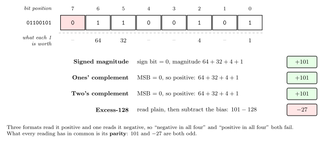
Figure 1: One bit pattern, four readings. Bits 6 down to 0 carry the same place values in every format, so the only question is what the leading bit is worth: nothing at all in signed magnitude, and a plain 0 in the two complement formats because it is clear. Excess-128 is the outlier - it reads the eight bits as plain unsigned and then takes the bias off the whole value, which is why the same pattern comes out negative there.
That immediately kills (a) and (b): the first three formats all read it as positive, but excess-128 reads it as \(-27\), so it is neither negative in all four nor positive in all four.
Parity is the property that does survive all four. In the three sign-magnitude-style formats the value is \(\pm 101\), which is odd; in excess-128 it is \(-27\), also odd. So (c) is true and (d) is false. See binary-number-representations.
Q5 — Reading a gate-level circuit
Which of the following logic circuits is an implementation of the function \(A \cdot (B \oplus C) \cdot D\)?
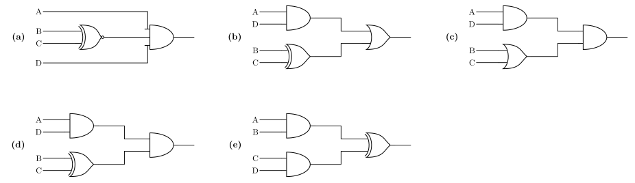
Figure 2: Question 5’s five candidate circuits. (a) is a three-input AND fed by A, an XNOR of B and C, and D; (b)–(e) each combine two two-input gates into a third.
- None of the above
TipAnswer
(d)
Read each circuit out as an expression:
| Option | Circuit | Function |
|---|---|---|
| (a) | 3-input AND of A, XNOR(B,C) and D | \(A \cdot \overline{(B \oplus C)} \cdot D\) |
| (b) | AND(A,D) and XOR(B,C) into an OR | \(A \cdot D + (B \oplus C)\) |
| (c) | AND(A,D) and OR(B,C) into an AND | \(A \cdot D \cdot (B + C)\) |
| (d) | AND(A,D) and XOR(B,C) into an AND | \(A \cdot D \cdot (B \oplus C)\) |
| (e) | AND(A,B) and AND(C,D) into an XOR | \((A \cdot B) \oplus (C \cdot D)\) |
AND is associative and commutative, so (d)’s \(A \cdot D \cdot (B \oplus C)\) is the same function as the target \(A \cdot (B \oplus C) \cdot D\).
The two near misses are worth naming. (a) has the right shape but the middle gate carries an output bubble, making it XNOR rather than XOR — the exact complement of what is wanted. (b) has both correct sub-gates but joins them with OR instead of AND. See logic-gates.
Q6 — Gate equivalence and De Morgan
Which of the following circuits is equivalent to:
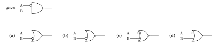
Figure 3: Question 6’s given circuit (top) and its four candidate equivalents. The given circuit is an AND gate with its A input inverted; each candidate is a single two-input gate with bubbles on some of its terminals.
- None of the above
TipAnswer
(b)
The given circuit is an AND with a bubble on its A input, so it computes
\[F = \overline{A} \cdot B\]
Push that through De Morgan’s law to get an OR-shaped form:
\[\overline{A} \cdot B = \overline{\overline{\overline{A} \cdot B}} = \overline{A + \overline{B}}\]
That is a gate with a bubble on the B input and a bubble on the output — an OR body with both, which is exactly option (b).
Checking the rest: (a) is the same gate without the output bubble, so \(A + \overline{B}\); (d) is an OR with the A input inverted, \(\overline{A} + B\); and (c) is an XNOR with A inverted, \(\overline{\overline{A} \oplus B} = A \oplus B\). None of those equals \(\overline{A} \cdot B\). See boolean-algebra and logic-gates.
Q7 — Boolean simplification
Which of the following logic functions is identical to \(\overline{\overline{(\overline{A} + \overline{B})} \cdot \overline{C} + \overline{B}}\)?
0
\(AC + \overline{B}\)
\(AB + \overline{B}C\)
\(\overline{A}B + BC\)
None of the above
TipAnswer
(d)
Work outwards from the innermost bar. The inner complement is a straight De Morgan:
\[\overline{\overline{A} + \overline{B}} = A \cdot B\]
so the expression under the long outer bar is \(A B \overline{C} + \overline{B}\). That simplifies by the absorption identity \(X \cdot Y + \overline{X} = Y + \overline{X}\), taking \(X = B\) and \(Y = A\overline{C}\):
\[B \cdot (A\overline{C}) + \overline{B} = A\overline{C} + \overline{B}\]
Now apply the outer bar:
\[\overline{A\overline{C} + \overline{B}} = \overline{A\overline{C}} \cdot B = (\overline{A} + C) \cdot B = \overline{A}B + BC\]
which is option (d).
Checking a couple of rows against the original settles it. With \(A=0, B=1, C=0\) the inside is \(0 \cdot 1 \cdot 1 + 0 = 0\), so the whole expression is 1, and (d) gives \(\overline{A}B = 1\). With \(A=1, B=1, C=0\) the inside is \(1 \cdot 1 \cdot 1 + 0 = 1\), so the expression is 0, and (d) gives \(0 + 0 = 0\). See boolean-algebra.
Q8 — Truth table to sum of products
Consider the logic function represented by the following truth table:
| A | B | C | X |
|---|---|---|---|
| 0 | 0 | 0 | 1 |
| 0 | 0 | 1 | 0 |
| 0 | 1 | 0 | 0 |
| 0 | 1 | 1 | 0 |
| 1 | 0 | 0 | 1 |
| 1 | 0 | 1 | 1 |
| 1 | 1 | 0 | 0 |
| 1 | 1 | 1 | 0 |
Which of the following expressions is equivalent to the function represented in this table?
\(X = A + B + C\)
\(X = A\overline{B}.\overline{C} + \overline{A}.\overline{B}.C + \overline{A}.B.\overline{C}\)
\(X = \overline{A}.B.\overline{C} + \overline{A}.B.C + \overline{A}.\overline{B}.\overline{C}\)
\(X = \overline{A.B.C}\)
None of the above
TipAnswer
(e)
The table has \(X = 1\) on exactly three rows: \(ABC = 000\), \(100\) and \(101\). Writing one product term per row,
\[X = \overline{A}\,\overline{B}\,\overline{C} + A\,\overline{B}\,\overline{C} + A\,\overline{B}\,C = \overline{B}\,\overline{C} + A\overline{B} = \overline{B}(\overline{C} + A)\]
Now check each option against those three minterms:
| Option | Minterms it covers (\(ABC\)) | Matches? |
|---|---|---|
| (a) \(A+B+C\) | everything except 000 | no — it is 0 exactly where the table is 1 |
| (b) \(A\overline{B}\overline{C} + \overline{A}\overline{B}C + \overline{A}B\overline{C}\) | 100, 001, 010 | no — 001 and 010 are 0 in the table |
| (c) \(\overline{A}B\overline{C} + \overline{A}BC + \overline{A}\,\overline{B}\,\overline{C}\) | 010, 011, 000 | no |
| (d) \(\overline{A \cdot B \cdot C}\) | everything except 111 | no — it is 1 on 001, which the table makes 0 |
None reproduces \(\{000, 100, 101\}\), so the answer is (e).
Option (b) is the closest — it shares the minterm 100 with the correct function and has the right number of terms — which is presumably the intended trap. See boolean-algebra.
Confirmed on review. “None of the above” is an unusual answer for a routine sum-of-products question, and it would also follow from a single mis-set bar in the source’s option (b). A second independent pass measured the bar positions in option (b) against the glyph positions at 1800 dpi: the bars sit over the first term’s B and C, the second term’s A and B, and the third term’s A and C, exactly as transcribed. Option (b) shares only the minterm 100 with the function, so it is two terms out, not one bar out, and (e) stands.
Q9 — Timing diagram to logic function
What logic function is represented by the following timing diagram?
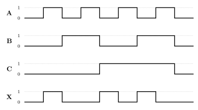
Figure 4: Question 9’s timing diagram. A, B and C step through all eight combinations — A toggling every interval, B every two, C every four — and X is the output to be identified.
\(X = \overline{C}.\overline{B}.A + \overline{C}.B.A + C.B.\overline{A}\)
\(X = \overline{C}.\overline{B}.\overline{A} + C.B.\overline{A} + \overline{C}.B.\overline{A}\)
\(X = C.\overline{B}.A + C.\overline{B} + C.\overline{A}\)
\(X = \overline{C}.\overline{B}.A + C.\overline{B}.\overline{A} + C.B.\overline{A}\)
None of the above
TipAnswer
(d)
A toggles every interval, B every two and C every four, so the eight intervals walk \(CBA\) through \(000, 001, 010, \ldots, 111\) in order. Read X off interval by interval:
| Interval | C | B | A | X |
|---|---|---|---|---|
| 1 | 0 | 0 | 0 | 0 |
| 2 | 0 | 0 | 1 | 1 |
| 3 | 0 | 1 | 0 | 0 |
| 4 | 0 | 1 | 1 | 0 |
| 5 | 1 | 0 | 0 | 1 |
| 6 | 1 | 0 | 1 | 0 |
| 7 | 1 | 1 | 0 | 1 |
| 8 | 1 | 1 | 1 | 0 |
One product term per high interval:
\[X = \overline{C}\,\overline{B}\,A + C\,\overline{B}\,\overline{A} + C\,B\,\overline{A}\]
which is option (d) exactly, term for term. See timing-diagrams.
Q10 — XOR identities
Which of the following logic functions is identical to \(A \oplus \overline{B}\)?
\(A.\overline{B} + \overline{A}.B\)
\(\overline{A}.\overline{B} + \overline{A}.B + A.B\)
\(A + \overline{B}\)
\(\overline{A \oplus B}\)
None of the above
TipAnswer
(d)
Inverting one input of an XOR inverts its output — this is the standard identity \(A \oplus \overline{B} = \overline{A \oplus B}\), which is option (d) as written.
To see it rather than quote it, expand:
\[A \oplus \overline{B} = A\,\overline{\overline{B}} + \overline{A}\,\overline{B} = A B + \overline{A}\,\overline{B}\]
That is 1 exactly when A and B agree, which is the definition of XNOR, i.e. \(\overline{A \oplus B}\).
The others: (a) is plain \(A \oplus B\), the complement of what is wanted; (b) simplifies as \(\overline{A}(\overline{B} + B) + AB = \overline{A} + AB = \overline{A} + B\), which fails at \(A=0, B=1\) (it gives 1, the target gives 0); (c) \(A + \overline{B}\) fails at \(A=1, B=0\) (it gives 1, the target gives 0). See boolean-algebra.
Q11 — NOR-only implementation
Which of the following circuits is a NOR-gate only implementation of the following function:
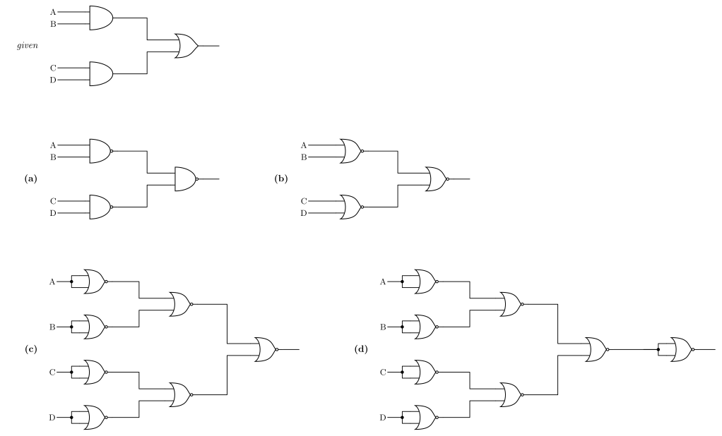
Figure 5: Question 11’s given function A.B + C.D (top) and its four candidate implementations. In (c) and (d) the NOR gates with both inputs tied together are acting as inverters; (d) has one more of them than (c).
- None of the above
TipAnswer
(d)
The function to reproduce is \(F = A \cdot B + C \cdot D\).
A NOR gate with both inputs tied together is an inverter, since \(\overline{X + X} = \overline{X}\) — that is what the small gates on the left of (c) and (d) are. With inverters available, a NOR fed by two complemented inputs is an AND:
\[\overline{\overline{A} + \overline{B}} = A \cdot B\]
So in both (c) and (d) the two middle NORs produce \(A \cdot B\) and \(C \cdot D\), and the NOR that joins them produces
\[\overline{A B + C D} = \overline{F}\]
which is the complement of what is wanted. (c) stops there and is therefore wrong. (d) adds one more tied-input NOR on the output, inverting once more to give \(F\) itself — so (d) is the NOR-only implementation.
The other two: (a) is a correct implementation of \(A B + C D\), but built from NAND gates, not NOR; (b) is three NOR gates in the same shape as the given circuit, which computes \(\overline{\overline{A+B} + \overline{C+D}} = (A+B)(C+D)\), a different function. See boolean-algebra and logic-gates.
Q12 — NOR latch behaviour
Which truth table correctly captures the behaviour of the following latch circuit?
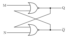
Figure 6: Question 12’s latch: two cross-coupled NOR gates. M is the external input to the gate that drives Q, N the input to the gate that drives Q-bar, and each gate’s output feeds back to the other gate’s second input.
| M | N | Q | \(\overline{Q}\) |
|---|---|---|---|
| 0 | 0 | Q | \(\overline{Q}\) |
| 0 | 1 | 0 | 1 |
| 1 | 0 | 1 | 0 |
| 1 | 1 | 0 | 0 |
| M | N | Q | \(\overline{Q}\) |
|---|---|---|---|
| 0 | 0 | Q | \(\overline{Q}\) |
| 0 | 1 | 1 | 0 |
| 1 | 0 | 0 | 1 |
| 1 | 1 | 1 | 1 |
| M | N | Q | \(\overline{Q}\) |
|---|---|---|---|
| 0 | 0 | Q | \(\overline{Q}\) |
| 0 | 1 | 0 | 1 |
| 1 | 0 | 1 | 0 |
| 1 | 1 | 1 | 1 |
| M | N | Q | \(\overline{Q}\) |
|---|---|---|---|
| 0 | 0 | Q | \(\overline{Q}\) |
| 0 | 1 | 1 | 0 |
| 1 | 0 | 0 | 1 |
| 1 | 1 | 0 | 0 |
- None of the above
TipAnswer
(d)
This is the standard cross-coupled NOR latch, so M behaves as the reset input and N as the set input — note which output each drives: M feeds the gate whose output is Q, so asserting M forces Q low.
Writing the two gate equations,
\[Q = \overline{M + \overline{Q}} \qquad \overline{Q} = \overline{N + Q}\]
and working through the four input combinations:
| M | N | Working | Q | \(\overline{Q}\) |
|---|---|---|---|---|
| 0 | 0 | both NORs just invert their feedback, so the state holds | Q | \(\overline{Q}\) |
| 0 | 1 | N = 1 forces the lower NOR’s output to 0, so \(\overline{Q} = 0\); the upper NOR then sees \(0 + 0\) and outputs 1 | 1 | 0 |
| 1 | 0 | M = 1 forces the upper NOR’s output to 0, so \(Q = 0\); the lower NOR sees \(0 + 0\) and outputs 1 | 0 | 1 |
| 1 | 1 | a 1 on either NOR forces its output low, so both outputs go to 0 | 0 | 0 |
That is option (d). The distinguishing rows are the middle two — (a) and (c) have them the wrong way round, treating M as set rather than reset — and the last row, where (b) and (c) claim both outputs go to 1 rather than 0. In a NOR latch the forbidden combination drives both outputs low; it is the NAND latch that drives them both high. See flip-flops-and-latches.
Q13 — D flip-flop timing
For the flip-flop circuit below and the given CLK and A values over time, which of the diagrams below best shows the Q output?
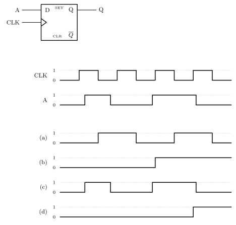
Figure 7: Question 13’s positive-edge-triggered D flip-flop, the CLK and A waveforms driving it, and the four candidate Q outputs (a) to (d).
- None of the above
TipAnswer
(b)
The clock input is drawn with a plain triangle and no bubble, so the flip-flop is positive-edge-triggered: Q takes the value of A at each rising edge of CLK and holds it until the next one.
There are four rising edges. Reading A at each:
| Rising edge | A at that instant | Q after |
|---|---|---|
| 1st | 0 — A does not go high until just after this edge | 0 |
| 2nd | 0 — A has already fallen | 0 |
| 3rd | 1 — A goes high just before this edge | 1 |
| 4th | 1 — A is still high | 1 |
So Q sits at 0 through the first two edges, rises at the third and stays high. That is exactly diagram (b), whose transition lands on the third rising edge.
The distractors are instructive. (c) is A itself, which is what a transparent latch would give rather than an edge-triggered flip-flop. (a) is what a negative-edge-triggered flip-flop would give: sampling on the falling edges catches A high at the first and third of them. (d) rises one clock too late, at the fourth edge. See flip-flops-and-latches and timing-diagrams.
Q14 — Two’s complement addition
What’s the result of adding the 5-bit two’s complement numbers 11101 and 01001?
00110
00111
01100
10110
10111
TipAnswer
(a)
Add the bit patterns as if they were unsigned and discard anything past bit 4 — that is the whole point of two’s complement:
\[\begin{array}{r} 11101 \\ +\;01001 \\ \hline 1\,00110 \end{array}\]
Dropping the carry out of the top bit leaves 00110, which is option (a).
The decimal check: 11101 has its sign bit set, so its magnitude is \(\overline{11101} + 1 = 00010 + 1 = 00011 = 3\), i.e. it is \(-3\). 01001 is \(+9\). And \(-3 + 9 = 6 = 00110_2\). The signs differ, so overflow is impossible here and the discarded carry is harmless. See binary-number-representations.
Q15 — Detecting overflow
Which of the following operations will result in an overflow in 5-bit two’s complement arithmetic?
10010+00010
10010–00010
01000+01010
01000–01010
None of the above
TipAnswer
(c)
A 5-bit two’s complement word covers \(-16\) to \(+15\). Overflow means the true result falls outside that range, which can only happen when two operands of the same sign are added (or operands of opposite sign are subtracted).
| Option | Decimal | Result | In range \([-16, 15]\)? |
|---|---|---|---|
| (a) | \(-14 + 2\) | \(-12\) | yes — and adding a positive to a negative can never overflow |
| (b) | \(-14 - 2\) | \(-16\) | yes — \(-16\) is exactly the most negative representable value |
| (c) | \(8 + 10\) | \(18\) | no — 18 > 15, so this overflows |
| (d) | \(8 - 10\) | \(-2\) | yes |
Option (b) is the near miss worth checking carefully: \(-16\) sits right on the boundary and is representable, as 10000. Only (c) leaves the range. See binary-number-representations.
Q16 — Overflow on a positive sum
Consider the binary addition operation 0111 + 0001. Which of the following statements is true if the numbers are interpreted as two’s complement?
The result is negative and no overflow occurs
The result should be negative but overflow occurs
The result is positive and no overflow occurs
The result should be positive but overflow occurs
The result is zero
TipAnswer
(d)
These are 4-bit two’s complement numbers, so the range is \(-8\) to \(+7\).
\[0111_2 = +7, \qquad 0001_2 = +1\]
The bit-level sum is
\[\begin{array}{r} 0111 \\ +\;0001 \\ \hline 1000 \end{array}\]
and 1000 read as 4-bit two’s complement is \(-8\). The true answer \(+8\) is one past the top of the range, so it cannot be represented: the addition of two positives has produced a negative pattern, which is the textbook overflow signature. The result should be positive but overflow has occurred — option (d).
Note that no carry leaves the top bit here, which is why “carry out” alone is not an overflow test in signed arithmetic; the test is the sign pattern of the operands versus the result. See binary-number-representations.
Q17 — Programming a multiplexer
Consider the following multiplexer. What must the inputs A,B,C,D be so that the multiplexer implements the function \(X = S_1 \oplus S_0\)?
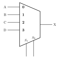
Figure 8: Question 17’s 4-to-1 multiplexer. A, B, C and D are wired to data inputs 0 to 3; S1 and S0 are the select lines, and X is the output.
A=1, B=1, C=1, D=1
A=1, B=0, C=0, D=1
A=0, B=1, C=1, D=0
A=1, B=1, C=0, D=0
None of the above
TipAnswer
(c)
A multiplexer used this way is a lookup table: the select lines index a data input, and that input’s constant value becomes the output. So each data input holds one row of the truth table of the function being built, with \(S_1\) as the high-order select bit.
| \(S_1\) | \(S_0\) | Input selected | \(S_1 \oplus S_0\) | So that input must be |
|---|---|---|---|---|
| 0 | 0 | 0 (A) | 0 | A = 0 |
| 0 | 1 | 1 (B) | 1 | B = 1 |
| 1 | 0 | 2 (C) | 1 | C = 1 |
| 1 | 1 | 3 (D) | 0 | D = 0 |
That is \(A=0, B=1, C=1, D=0\) — option (c). Swapping which select line is the high bit changes nothing here, because XOR is symmetric in its two inputs, so (c) is the answer either way. The distractors are different functions: (d) is 1 on the two inputs reached when \(S_1 = 0\) and 0 on the other two, i.e. \(\overline{S_1}\) — what you get by reading only the high select bit — and (b) is the XNOR, the complement of the target. See combinational-logic-blocks.
Q18 — Shift register with hold
Which of the following statements about this shift register circuit is true?
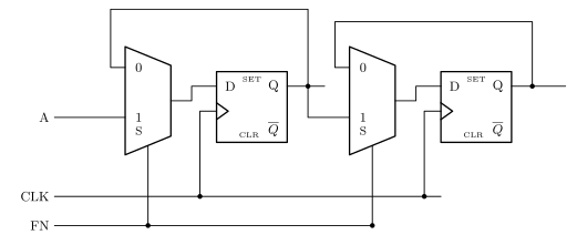
Figure 9: Question 18’s two-stage shift register. Each stage is a 2-to-1 multiplexer feeding a D flip-flop: input 1 of each multiplexer takes the data from the left, input 0 takes that stage’s own Q back again, and FN drives both selects.
When A is 1, data will be shifted to the right on every rising clock edge
When A is 0, data will be shifted to the right on every rising clock edge
When FN is 1, data will be shifted to the left on every rising clock edge
When FN is 0, the flip-flops will maintain their values (even if the circuit is clocked)
None of the above
TipAnswer
(d)
Trace what each multiplexer feeds its flip-flop:
- Input 1 of the first multiplexer is A, and input 1 of the second is the first stage’s Q. So with the selects at 1, the chain is \(A \to \text{FF}_1 \to \text{FF}_2\) — data moves one stage to the right per clock.
- Input 0 of each multiplexer is that stage’s own Q, looped back over the top. So with the selects at 0, each flip-flop is reloaded with the value it already holds, and nothing changes even though the clock keeps running.
Both selects are driven by FN, so FN chooses shift (1) or hold (0), and A is data, not control. That makes (d) true: with FN = 0 the flip-flops maintain their values through any number of clock edges.
The others fail because A is a data input, not a mode control — (a) and (b) confuse the two — and because the connection order runs left to right, so FN = 1 shifts right, not left, killing (c).
This “recirculating” pattern is the standard way to add a hold or enable to a register without gating the clock, which would risk glitches. See shift-registers.
Q19 — Counter width
What’s the minimum number of flip-flops needed to build a synchronous binary counter capable of counting from 0 to 32 (inclusive)?
5
6
7
32
33
TipAnswer
(b)
“0 to 32 inclusive” is 33 distinct values, not 32 — that off-by-one is the whole question. Each flip-flop holds one bit, and \(n\) flip-flops give \(2^n\) states, so we need the smallest \(n\) with
\[2^n \ge 33\]
\(2^5 = 32\), which is one short; \(2^6 = 64\), which is enough. So six flip-flops — option (b).
Option (a) is the answer to “0 to 31”, which is the trap. See counters.
Q20 — Synchronous counter sequence
What sequence will the following synchronous counter count through?
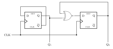
Figure 10: Question 20’s two-bit synchronous counter. The left flip-flop’s D input comes from its own Q-bar, so Q1 toggles every clock; the right flip-flop’s D input is the XNOR of Q1 and Q0. Both flip-flops share the clock.
\(Q_1Q_0\): \(00 \to 01 \to 10 \to 11 \to 00 \to \ldots\)
\(Q_1Q_0\): \(00 \to 10 \to 11 \to 01 \to 00 \to \ldots\)
\(Q_1Q_0\): \(00 \to 11 \to 01 \to 10 \to 00 \to \ldots\)
\(Q_1Q_0\): \(00 \to 01 \to 11 \to 10 \to 00 \to \ldots\)
None of the above
TipAnswer
(c)
Read the two excitation equations off the schematic. The left flip-flop’s D input is wired straight back to its own \(\overline{Q}\), and the right flip-flop’s D input is the XNOR of the two Q outputs:
\[D_1 = \overline{Q_1} \qquad D_0 = \overline{Q_1 \oplus Q_0}\]
Both flip-flops share the clock, so both update together from the current state. Starting at 00:
| \(Q_1 Q_0\) | \(D_1 = \overline{Q_1}\) | \(D_0 = \overline{Q_1 \oplus Q_0}\) | Next |
|---|---|---|---|
| 0 0 | 1 | \(\overline{0 \oplus 0} = 1\) | 1 1 |
| 1 1 | 0 | \(\overline{1 \oplus 1} = 1\) | 0 1 |
| 0 1 | 1 | \(\overline{0 \oplus 1} = 0\) | 1 0 |
| 1 0 | 0 | \(\overline{1 \oplus 0} = 0\) | 0 0 |
So the sequence is \(00 \to 11 \to 01 \to 10 \to 00\), option (c). All four states appear, so the counter is a valid four-state cycle — just not in binary order.
The gate identity is what to watch here: the bubble on the gate’s output makes it an XNOR, and an XOR there would have produced a different sequence entirely. See counters.
Q21 — State diagram to state table
Consider the state diagram below.
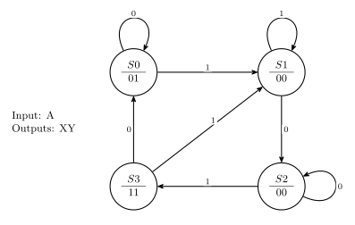
Figure 11: Question 21’s state diagram. Each state shows its name above the rule and its XY output below; the labels on the arrows are the values of the single input A.
Which of the following is an equivalent state table?
| Current State | Input (A) | Next State | Outputs (X,Y) |
|---|---|---|---|
| S0 | 0 | S0 | 01 |
| S0 | 1 | S1 | 01 |
| S1 | 0 | S1 | 00 |
| S1 | 1 | S2 | 00 |
| S2 | 0 | S2 | 00 |
| S2 | 1 | S3 | 00 |
| S3 | 0 | S0 | 11 |
| S3 | 1 | S1 | 11 |
| Current State | Input (A) | Next State | Outputs (X,Y) |
|---|---|---|---|
| S0 | 0 | S0 | 01 |
| S0 | 1 | S1 | 01 |
| S1 | 0 | S2 | 00 |
| S1 | 1 | S1 | 00 |
| S2 | 0 | S2 | 00 |
| S2 | 1 | S3 | 00 |
| S3 | 0 | S0 | 11 |
| S3 | 1 | S2 | 11 |
| Current State | Next State (A=0) | Next State (A=1) | Outputs (X,Y) |
|---|---|---|---|
| S0 | S0 | S1 | 01 |
| S1 | S2 | S1 | 00 |
| S2 | S2 | S3 | 00 |
| S3 | S0 | S1 | 11 |
| Current State | Next State (A=0) | Next State (A=1) | Outputs (X,Y) |
|---|---|---|---|
| S0 | S0 | S1 | 00 |
| S1 | S2 | S1 | 01 |
| S2 | S2 | S3 | 10 |
| S3 | S0 | S1 | 11 |
- None of the above
TipAnswer
(c)
Read the eight arrows off the diagram — every state has exactly two, one per value of A, which is completeness for a one-input machine:
| State | Output XY | A = 0 | A = 1 |
|---|---|---|---|
| S0 | 01 | self-loop, stays S0 | goes to S1 |
| S1 | 00 | goes down to S2 | self-loop, stays S1 |
| S2 | 00 | self-loop, stays S2 | goes across to S3 |
| S3 | 11 | goes up to S0 | goes diagonally to S1 |
That is option (c), row for row.
Where each of the others goes wrong:
- (a) gets S1’s two arrows backwards — it makes S1 self-loop on 0 and go to S2 on 1, whereas the diagram has the self-loop labelled 1.
- (b) has the right S1 rows but sends S3 to S2 on A = 1; the diagonal arrow out of S3 goes to S1.
- (d) has the right next-state columns but the wrong outputs: it lists 00, 01, 10, 11 down the states, whereas the diagram gives 01, 00, 00, 11.
This is a Moore machine — the output is written inside each state bubble, so it depends only on the state and not on A, which is why (c) can fold the eight rows into four. See state-machines.
Q22 — Tracing a state machine
Consider the state machine represented by the state diagram in question 21 above (see Q21). What sequence of states is traversed if the machine starts in state S0 and A goes through the sequence 110011 (i.e. two 1’s followed by two 0’s followed by two 1’s)?
S0\(\to\)S1\(\to\)S2\(\to\)S2\(\to\)S3\(\to\)S1\(\to\)S1
S0\(\to\)S1\(\to\)S2\(\to\)S3\(\to\)S0\(\to\)S1\(\to\)S2
S0\(\to\)S1\(\to\)S1\(\to\)S2\(\to\)S2\(\to\)S3\(\to\)S3
S0\(\to\)S1\(\to\)S2\(\to\)S3\(\to\)S1\(\to\)S2\(\to\)S3
S0\(\to\)S1\(\to\)S1\(\to\)S2\(\to\)S2\(\to\)S3\(\to\)S1
TipAnswer
(e)
Feed the six input bits into the table derived in Q21, one transition per bit, starting from S0:
| Step | Input A | From | To |
|---|---|---|---|
| 1 | 1 | S0 | S1 |
| 2 | 1 | S1 | S1 (self-loop on 1) |
| 3 | 0 | S1 | S2 |
| 4 | 0 | S2 | S2 (self-loop on 0) |
| 5 | 1 | S2 | S3 |
| 6 | 1 | S3 | S1 |
Including the starting state, the traversal is
\[S0 \to S1 \to S1 \to S2 \to S2 \to S3 \to S1\]
which is option (e). The two self-loops are what separate it from the distractors: (a) and (b) skip them, and (c) has the right shape but ends with a self-loop on S3, which the diagram does not have — S3’s arrows both leave. See state-machines.
Q23 — Tanenbaum ALU bit slice
Consider the ALU bit slice below (from the Tanenbaum textbook, also shown in lectures)
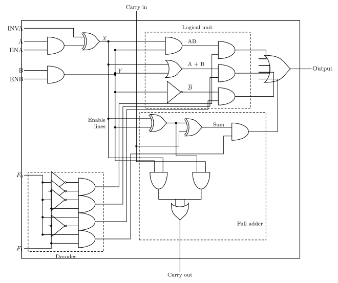
Figure 12: Question 23’s ALU bit slice, the one from Tanenbaum. ENA, INVA and ENB condition A and B into the internal signals X and Y; the logical unit computes AB, A + B and B-bar from them and the full adder computes their sum; a two-to-four decoder driven by F0 and F1 raises exactly one enable line, so exactly one of the four results reaches the output OR.
For the ALU bit slice above, under what conditions will the ALU output be \(A\)?
ENA = 0, ENB = 0, INVA = 1, F\(_0\) = 1, F\(_1\) = 0, Carry in = 0
ENA = 1, ENB = 1, INVA = 1, F\(_0\) = 0, F\(_1\) = 0, Carry in = 0
ENA = 1, ENB = 0, INVA = 1, F\(_0\) = 0, F\(_1\) = 1, Carry in = 0
ENA = 1, ENB = 0, INVA = 0, F\(_0\) = 1, F\(_1\) = 1, Carry in = 0
None of the above
TipAnswer
(d)
Two things have to be worked out for every option: what the conditioning gates make of A and B, and which of the four function blocks the decoder enables.
The conditioning is read straight off the left of the figure:
\[X = (A \cdot \text{ENA}) \oplus \text{INVA} \qquad\qquad Y = B \cdot \text{ENB}\]
and the decoder’s four outputs pick the function in Tanenbaum’s order:
| \(F_0\) | \(F_1\) | Function selected |
|---|---|---|
| 0 | 0 | \(X\) AND \(Y\) |
| 0 | 1 | \(X\) OR \(Y\) |
| 1 | 0 | \(\overline{Y}\) |
| 1 | 1 | \(X + Y + \text{Carry in}\) (the adder) |
Now evaluate each option:
| Option | \(X\) | \(Y\) | Function | Output |
|---|---|---|---|---|
| (a) | ENA=0, INVA=1 \(\Rightarrow\) 1 | ENB=0 \(\Rightarrow\) 0 | \(\overline{Y}\) | \(\overline{0} = 1\) |
| (b) | ENA=1, INVA=1 \(\Rightarrow\) \(\overline{A}\) | ENB=1 \(\Rightarrow\) \(B\) | AND | \(\overline{A} \cdot B\) |
| (c) | ENA=1, INVA=1 \(\Rightarrow\) \(\overline{A}\) | ENB=0 \(\Rightarrow\) 0 | OR | \(\overline{A} + 0 = \overline{A}\) |
| (d) | ENA=1, INVA=0 \(\Rightarrow\) \(A\) | ENB=0 \(\Rightarrow\) 0 | adder | \(A + 0 + 0 = A\) |
Only (d) gives \(A\).
It is worth noticing why (d) works: the adder with one input forced to zero and no carry in is just a pass-through, so the arithmetic unit can move A to the output as easily as the logical unit can. The more familiar recipe from the combinations table — select OR, pass A, force the other side to zero — is not on offer here, since no option pairs \(F_0 = 0, F_1 = 1\) with INVA = 0. See arithmetic-logic-unit for the full table of useful control combinations.
Q24 — ALU bit slice with an 8-way mux
Consider the ALU bit slice below.
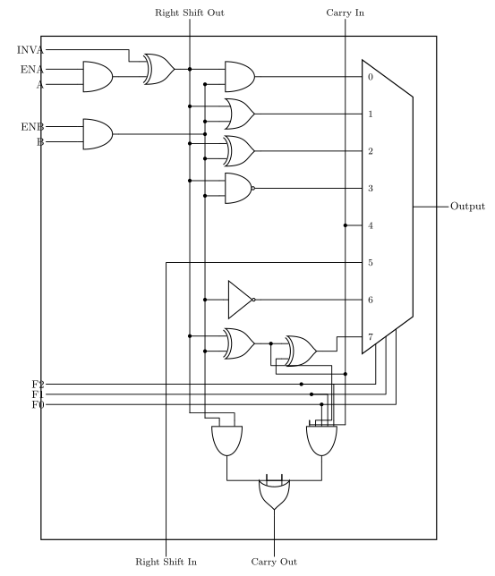
Figure 13: Question 24’s ALU bit slice. X = (A.ENA) xor INVA and Y = B.ENB feed eight candidate results; the multiplexer selects one under F2 F1 F0, giving in order X.Y, X + Y, X xor Y, NOT(X.Y), the carry in, the right shift in, Y-bar, and the full adder’s sum. The carry out is X.Y or the propagate term, which is gated so it only passes in add mode.
For an ALU made up of 8 of the bit slices above, which of the following control input settings will result in the ALU output being \(A - 1\)? (The “Right Shift In” control input refers to that for the most significant bit; the “Carry in” control input refers to that for the least significant bit.)
ENA = 1, ENB = 0, INVA = 0, F\(_2\) = 1, F\(_1\) = 1, F\(_0\) = 1, Right Shift In = 0, Carry in = 0
ENA = 1, ENB = 0, INVA = 1, F\(_2\) = 1, F\(_1\) = 1, F\(_0\) = 1, Right Shift In = 0, Carry in = 0
ENA = 1, ENB = 0, INVA = 0, F\(_2\) = 1, F\(_1\) = 1, F\(_0\) = 1, Right Shift In = 0, Carry in = 1
ENA = 1, ENB = 0, INVA = 1, F\(_2\) = 1, F\(_1\) = 1, F\(_0\) = 1, Right Shift In = 0, Carry in = 1
None of the above
TipAnswer
(e)
The conditioning is the same as in Q23:
\[X = (A \cdot \text{ENA}) \oplus \text{INVA} \qquad\qquad Y = B \cdot \text{ENB}\]
and the multiplexer’s eight inputs, in order, are
| \(F_2 F_1 F_0\) | Output |
|---|---|
| 000 | \(X \cdot Y\) |
| 001 | \(X + Y\) |
| 010 | \(X \oplus Y\) |
| 011 | \(\overline{X \cdot Y}\) |
| 100 | Carry in |
| 101 | Right Shift In |
| 110 | \(\overline{Y}\) |
| 111 | \(X + Y + \text{Carry in}\) (the full adder’s sum) |
Every option sets \(F_2 F_1 F_0 = 111\), so every option is doing arithmetic, and every option sets ENB = 0, so \(Y = 0\) across the whole word. That reduces the adder to \(X + 0 + C_{in}\), and there are only four things it can produce:
| Option | INVA | \(X\) | \(C_{in}\) | Result |
|---|---|---|---|---|
| (a) | 0 | \(A\) | 0 | \(A\) |
| (b) | 1 | \(\overline{A}\) | 0 | \(\overline{A}\), which is \(-A - 1\) |
| (c) | 0 | \(A\) | 1 | \(A + 1\) |
| (d) | 1 | \(\overline{A}\) | 1 | \(\overline{A} + 1\), which is \(-A\) |
None of them is \(A - 1\), so the answer is (e).
The reason is structural rather than a matter of picking the right row. \(A - 1\) means \(A + (-1)\), i.e. adding a word of all ones. The only way this slice can conjure a constant into the adder is through the B side, and B’s conditioning is just \(Y = B \cdot \text{ENB}\) — it can force Y to 0 or pass B through, but it can never force Y to 1. The A side can be forced to all ones (ENA = 0, INVA = 1), which is how \(B - 1\) is done, but there is no matching path to put A on the other adder input. Q25 is the same observation asked directly, and the two answers corroborate each other.
Q25 — What an ALU cannot compute
For the ALU in question 24 (see Q24), which of the following arithmetic operations can NOT be performed?
\(A + 1\)
\(B + 1\)
\(A - 1\)
\(B - 1\)
All of the above operations can be performed
TipAnswer
(c)
Work through the four operations using \(X = (A \cdot \text{ENA}) \oplus \text{INVA}\), \(Y = B \cdot \text{ENB}\) and the adder selected by \(F_2 F_1 F_0 = 111\):
| Operation | ENA | INVA | ENB | Carry in | \(X\) | \(Y\) | Sum |
|---|---|---|---|---|---|---|---|
| \(A + 1\) | 1 | 0 | 0 | 1 | \(A\) | 0 | \(A + 1\) ✓ |
| \(B + 1\) | 0 | 0 | 1 | 1 | 0 | \(B\) | \(B + 1\) ✓ |
| \(B - 1\) | 0 | 1 | 1 | 0 | all ones \(= -1\) | \(B\) | \(B - 1\) ✓ |
| \(A - 1\) | ? | ? | ? | ? | see below |
The three that work draw on two mechanisms, and both of them live on the A side or on the carry. A \(+1\) comes free as the carry into the least significant slice, which is how \(A + 1\) and \(B + 1\) are built. A \(-1\) has to be an operand of all ones, and the only place one can be conjured is the A path: setting ENA = 0 and INVA = 1 forces X to all ones, which is \(-1\) in two’s complement, and that is how \(B - 1\) is built.
\(A - 1\) needs the mirror image — A itself on one adder input and \(-1\) on the other — and the B side cannot produce a constant. \(Y = B \cdot \text{ENB}\) is either \(B\) or zero, never all ones, and there is no inverter on the B path to make it one. So \(A - 1\) cannot be done in a single pass, and the answer is (c).
Note the asymmetry is deliberate in this style of ALU: only one operand needs constant-generating hardware, because \(B - A\), \(B - 1\) and \(-1\) all fall out of putting it on the A side. See arithmetic-logic-unit, whose table of useful control combinations shows the same pattern.
Your score
Reload the page to clear your answers.