CSSE2010 — Week 6 Notes
Lecture 11 — Instruction Set Architecture Part 1
The ISA is a document, and this is what is in the document. See instruction-set-architecture for the four-part frame, memory-models for the first part in full, avr-architecture for the register file and avr-io-ports for the I/O registers.
The ISA as an interface
Machine code, the ISA as a specification, and a first look at the AVR are in 2026-08-27-avr-introduction. The split between specification and implementation, in the form the rest of the course leans on:
- The ISA defines the interface between hardware and software. The ISA is a specification; the microarchitecture is how the control unit is built.
- Hardware (microarchitecture) designers don’t need to know about the high level software. They just build a microarchitecture that implements the ISA.
- Software writers (machine language programmers and compiler writers) don’t need to know (much) about microarchitecture. They just write or generate instructions that match the ISA.
Picture software (SW) above, hardware (HW) below, and on the line between them a row of bits — 1 0 1 0 1. The interface is not an API or a protocol; it is a bit pattern, and both sides are built from the same document that says what the pattern means.
What makes an ISA?
Four things:
- Memory models
- Registers
- Instructions
- Data types
Parts 1 and 2 and the start of part 3 are below. Instructions continue and data types arrive in 2026-09-03-instruction-set-architecture-part-2. The payoff: if you know all these details you can write machine code that runs on the CPU, and build the CPU.
1. Memory models
The memory model is how memory looks to the CPU. There are four issues, better read as decisions the specification has to make than as problems to be solved:
- A. Addressable cell size
- B. Alignment
- C. Address spaces
- D. Endianness
Full treatment in memory-models.
Memory organisation
Computer memory is conceptually a set of addressable cells. Cells are usually 8 bits wide (one byte), though various cell widths have been used in the past. Drawn as a grid, the address indexes down the left and the cell width runs across.
Take a 4 × 3 memory: 4 addresses, 3-bit cells. \(2^2 = 4\), so two address bits name four cells.
At gate level that memory is built like this:
- One cell is a row of three D flip-flops.
- The address decoder turns
A1 A0into one row-select line.A1 A0 = 0 1selects row 1. WRITE= 1 gatesDATA IN(I2 I1 I0) into the selected row through the AND gates on the left. The selected row’s outputs reachDATA OUT(O2 O1 O0) through the AND-OR tree on the right.
Nothing new appears here: it is flip-flops-and-latches for the storage and combinational-logic-blocks for the selection. Memory is a decoder, some flip-flops and some gates. The whole schematic is in memory-models.
A. Addressable cell size
The most common cell size is 8 bits (1 byte), but not always. The AVR is the counterexample:
| AVR | Cell width |
|---|---|
| data | 8 bits |
| program | 16 bits |
The bus is used to transport the content of a cell. Sometimes the data bus is wider than a cell, i.e. it retrieves several cells (addresses) at once, and then the address bus does not need to be as wide.
Bus sizes
For every doubling of data bus width, remove the least significant bit of the address bus.
For \(2^n\) cells of 8 bits, the address size is \(n\) bits, and the configurations are:
| Data bus | Address bus | Transferred |
|---|---|---|
| 8 bits | \(n\) | one cell at a time |
| 16 bits | \(n-1\) | two cells at a time |
| 32 bits | \(n-2\) | four cells at a time |
A concrete case: a memory with addresses 000000, 000001, 000010, … up to 111111, each cell 8 bits wide.
\[64 \text{ cells} = 2^6 \implies 6 \text{ address bits}\]
Group the cells in pairs and then in fours, and the address bus A goes 6, 5, 4 bits as the data bus D goes 8, 16, 32.
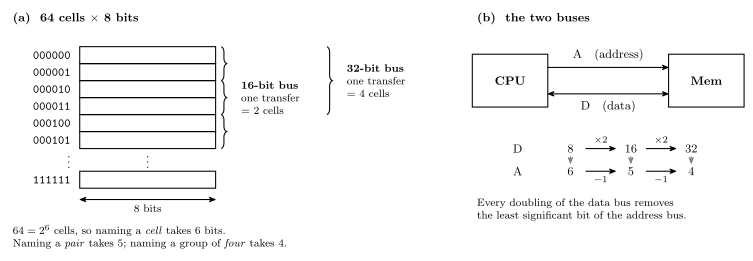
Figure 1: The bus-width trade-off. (a) 64 cells of 8 bits, so a cell needs a 6-bit address. A 16-bit data bus can only ever hand over an aligned pair of cells, and there are 32 pairs — 5 bits; a 32-bit bus hands over a group of four, and there are 16 groups — 4 bits. (b) the same fact read off the two buses at once: every doubling of D removes one bit from A.
Widening the data bus by a factor of two narrows the address bus by exactly one bit, because the transfer now names a group of cells rather than a cell.
Worked: address bus width
If a CPU supports \(2^{35}\) bytes of memory and has a 64 bit data bus, how many bits wide is the address bus?
32.
Start from the cell size. Cell = 8 bits, so \(2^{35}\) bytes is \(2^{35}\) cells, and a byte-at-a-time machine would need a 35-bit address. Then walk the ladder, doubling the data bus and dropping one address bit each time:
| Data bus | 8 | 16 | 32 | 64 |
|---|---|---|---|---|
| Address bus | 35 | 34 | 33 | 32 |
Three doublings from 8 to 64, so three bits off 35.
B. Alignment
Many architectures require natural alignment, e.g. 4-byte words starting at addresses 0, 4, 8, … and 8-byte words starting at 0, 8, 16, …
An 8-byte example, counting the reads:
| Reads | ||
|---|---|---|
| aligned — 8-byte word at address 8 | occupies exactly the block 8–15 | one |
| non-aligned — 8-byte word at address 12 | half in block 8–15, half in block 16–23 | two |
Alignment is often required because it is more efficient. The counter-example is the Pentium IV, which fetches 8 bytes at a time from memory (64-bit wide data bus) and for which alignment is not required, so the processor stays backwards compatible with earlier processors:
- a 4-byte word stored at address 4 takes 1 read (bytes 0 to 7);
- a 4-byte word stored at address 6 must read bytes 0 to 7 (one read) and bytes 8 to 15 (second read), then extract the 4 required bytes from the 16 bytes read.
Worked: counting reads
How many memory reads are needed to read an 8-byte value on a machine with a 16-bit data bus that does not require natural alignment?
4 or 5.
There are two cases, an even start address and an odd one:
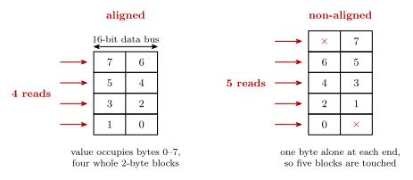
Figure 2: Reading an 8-byte value on a 16-bit data bus. Each row is one 2-byte block, i.e. one read; the numbers are the eight bytes of the value. Start the value at an even address and it fills four whole blocks — 4 reads. Start it at an odd address and one byte sits alone in the block at each end, so five blocks have to be read for eight bytes. Addresses increase upward and the higher-addressed byte of each block is drawn on the left. A × marks a byte in the fetched block that is not part of the value (csse2010-diagram-notation).
“Does not require” is the operative phrase — the machine permits both, so the answer has to cover both. That is why every question of this shape answers “\(k\) or \(k+1\)” rather than a single number.
C. Address spaces
Many microprocessors have a single linear memory address space — the von Neumann architecture — e.g. \(2^{32}\) bytes numbered from 0 to \(2^{32} - 1\) (which may not be bytes — it depends on the addressable cell size). Picture one strip with data at the low end and program at the high end: one space, shared.
The Harvard architecture has separate address spaces for instructions and data: two spaces, each starting at its own 0.
The AVR ATmega 324A is Harvard:
| Size | ||
|---|---|---|
| Data address space | \(2^{11}\) (2048) bytes | 2 kB, 8-bit cells |
| Instruction address space | \(2^{14}\) 16-bit words | 16,384 instruction words = 32,768 bytes |
The working:
\[2 \cdot 2^{10}\,\text{B} \to 2^{11} \text{ cells} \to 11 \text{ bits}\] \[2^{5} \cdot 2^{10}\,\text{B} = 2^{15}\,\text{B} \xrightarrow{\ \div 2\ } 2^{14} \text{ cells} \to 14 \text{ bits}\]
The \(\div 2\) is the step people drop. 32 kB of program memory is \(2^{15}\) bytes but only \(2^{14}\) addresses, because each address names a 16-bit cell. Convert to cells first, then take the logarithm.
The datasheet memory map fills that in — 32 registers, 64 I/O registers, 160 extended I/O registers and then 2 kB of SRAM up to 0x08FF on the data side; 0x0000 to 0x3FFF of Application and Boot flash on the program side. The map is in memory-models; the rest of the chip is in avr-architecture.
The \(2^{11}\) bytes is the size of the SRAM only. The data space itself runs to 0x08FF, which is that 2 kB plus the 256 locations (0x0000–0x00FF) the register file and the I/O registers occupy in front of it. The two I/O bands together hold 224 I/O registers, a number that comes back with the I/O registers below.
D. Endianness
Different machines may support different byte orderings.
| Which end goes at the lowest address | Who | |
|---|---|---|
| Little endian | the little end — least significant byte stored first | Intel microprocessors (Pentium etc.), AVR |
| Big endian | the big end stored first | SPARC, Freescale (formerly Motorola) microprocessors |
Most desktop/workstation/server CPUs produced since ~1992 are bi-endian (support both). Some are switchable at boot time, others at run time, i.e. can change dynamically.
Think of a read as SOURCE → TARGET: four memory cells at addresses \(m\), \(m+1\), \(m+2\), \(m+3\) are the source, a four-byte register is the target, and the bytes either cross over (little endian) or run straight across (big endian).
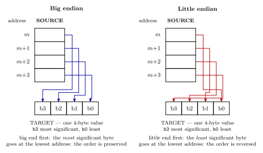
Figure 3: Assembling one 4-byte value out of four memory cells. The only difference between the two machines is which end of the value the lowest address holds. Big endian keeps the order (address \(m\) supplies the most significant byte); little endian reverses it. Nothing about the memory changes — the same four cells give two different values, and only the ISA says which.
Worked example
Given the memory:
| Address | Contents |
|---|---|
| 0 | 00001111 |
| 1 | 00110011 |
| 2 | 11011101 |
| 3 | 00101100 |
The 1-byte word at address 1 is 00110011 — one cell, so endianness does not enter into it.
The 2-byte word at address 0 on a big endian system is 00001111 00110011. Big end first, so address 0 holds the most significant byte and address 1 the least — the arrows run straight across.
Worked: the little endian read
With the memory above, what is the value of the 2-byte word at address 2 if this is a little endian system?
00101100 11011101.
Little end first, so address 2 (11011101) is the least significant byte and address 3 (00101100) the most — and writing the value out most-significant-first therefore reverses them.
There are two mistakes to make here, and only one of them is about endianness. Crossing them gives four candidate answers:
| Which word, read which way | ||
|---|---|---|
| A | 00110011 11011101 |
the word at address 1, read big-endian |
| B | 11011101 00110011 |
the word at address 1, read little-endian |
| C | 11011101 00101100 |
the right word, read big-endian |
| D | 00101100 11011101 |
✓ the right word, read little-endian |
So C is the endianness trap; A and B are the off-by-one trap, both dragging in 00110011 from address 1, which is not part of this word at all.
The reliable procedure: list the addresses the value occupies in increasing order, then assemble the answer most significant byte first. Big endian reads that list forwards, little endian backwards.
2. Registers
There are two types of register:
- General purpose — used for temporary results etc. On the AVR these are r0 … r31.
- Special purpose, e.g. Program Counter (PC), Stack pointer (SP), Input/Output Registers (224 on the AVR), Status Register (flags N Z C V; Tanenbaum calls this the Program Status Word).
Some other registers are part of the microarchitecture, not the ISA — e.g. the Instruction Register (IR). The programmer doesn’t need to know about these, and can’t directly change or use them.
That is the line the ISA draws. The IR exists, holds the instruction, and is in the CPU diagram of avr-architecture — but no instruction names it, so it is not in the specification and a chip designer may do as they like with it. The PC is in the specification because jmp writes it.
AVR registers
The general purpose registers (0–31) are quite regular and can be used interchangeably, with two exceptions:
- A few instructions work on half the registers (registers 16–31). Only 4 bits are used to represent the operand in the instruction, and \(2^4 = 16\). This is the same fact that restricts
LDI, seen from the encoding side (avr-instructions). - The X, Y, Z registers, below.
There are also many I/O registers (224). They are not to be confused with the general purpose registers: some instructions work with I/O registers, others with general purpose registers.
X, Y and Z
The top six registers of the register file pair off into three pointers, listed here with their register addresses:
| Pointer | Pair | Register addresses |
|---|---|---|
| X | R27 : R26 | 0x1B : 0x1A |
| Y | R29 : R28 | 0x1D : 0x1C |
| Z | R31 : R30 | 0x1F : 0x1E |
So Z ≡ R31 : R30. Two 8-bit registers side by side make a 16-bit address, which is what a data space wider than 256 bytes needs and no single register can hold. See avr-architecture.
AVR I/O registers
The AVR ATmega324A has 224 I/O register addresses, used to control peripherals and get data to/from them:
- Timers and counters
- Analog to digital converters
- Serial input/output
- General purpose input/output ports
- Each port (x = A, B, C or D) has three registers: DDRx (data direction register), PORTx (values to output), PINx (values on the pins). See learning lab 11.
Some addresses are reserved (not actually available on this device). Everything about these is in avr-io-ports — and the three port registers turn up a lab early, in week6-lab-avr-io-ports.
3. Instructions
Instructions are the main feature of an ISA. Instruction types include:
| Input/Output | communicate with I/O devices |
| Load/Store | move data from/to memory |
| Move | copy data between registers |
| Arithmetic | addition, subtraction, … |
| Logical | Boolean operations |
| Branching | for deciding which instruction to perform next |
The instructions met so far: MOV rd, rr (copy, not move), ADD rd, rr, AND/OR/EOR rd, rr, and LDI rd, K for r16–r31 (avr-instructions).
Input/output instructions
The 224 I/O registers split into two classes by how you are allowed to reach them:
| Where | Reached by | |
|---|---|---|
| I/O registers 0 to 223 | data memory addresses 32 to 255 ($20 to $FF) |
load and store instructions |
| First 64 (0 to 63) — special | also in and out |
|
| Other 160 (64 to 223) — “extended” I/O registers | load and store only |
Data memory, lowest addresses first, is r0 … r31, then the 64 I/O registers, then the 160 extended I/O registers. That is where the $20 offset comes from: the register file is in the way.
IN and OUT
in rd, P |
Load I/O register value into general purpose register | rd: r0 to r31; P = I/O register number (0 to 63, 0 to 0x3F) |
out P, rr |
Store value from general purpose register into I/O register | rr: r0 to r31; P = 0 to 63 (0 to 0x3F) |
One example of each:
\[\texttt{IN r0, 0} \;\equiv\; \texttt{IN r0, PINA}\] \[\texttt{OUT 1, r0} \;\equiv\; \texttt{OUT DDRA, r0}\]
Picture the CPU holding r0 … r31 on one side and the 64 I/O registers on the other. IN is a read of an I/O register and OUT is a write to one. avr-io-ports draws the pair with one arrow each way.
Two things to take from those two lines. The number and the name are the same operand — I/O register 0 is PINA and I/O register 1 is DDRA, and the name only exists because m324Adef.inc was included. And the destination is written first in both, which is why the I/O register moves from second operand to first between them. Both instructions are one word and one clock cycle. Full detail in avr-io-ports.
Summary
The four parts of an ISA:
- Memory models ✓
- Registers ✓
- Instructions — more in Lecture 12
- Data types — Lecture 12
If you know all these details, you can write machine code that runs on the CPU and build the CPU.
See also
- memory-models — cell size, alignment, address spaces, endianness in full
- instruction-set-architecture · avr-architecture · avr-io-ports · avr-instructions
- flip-flops-and-latches · combinational-logic-blocks — what the 4 × 3 memory is built from
- 2026-08-27-avr-introduction — Lecture 10
- 2026-09-03-instruction-set-architecture-part-2 — Lecture 12
- week6-lab-avr-io-ports — Lab 10, where
inandoutget used
Lecture 12 — Instruction Set Architecture Part 2
The second half of “what makes an ISA”: the rest of the instructions, the addressing modes, and data types. See avr-instructions for the instruction set as a reference, addressing-modes for the four modes and instruction-set-architecture for the frame.
The four parts of an ISA
The four-part list from 2026-08-31-instruction-set-architecture-part-1, with the lecture each part belongs to:
| 1. Memory models — A. addressable cell size, B. alignment, C. address spaces, D. endianness | Lecture 11 | |
| 2. Registers | Lecture 11 | |
| 3. Instructions | Lecture 12 | |
| 4. Data types | Lecture 12 |
3. Instructions
Instructions are the main feature of an ISA. There are five types. Unlike the list in Lecture 11, arithmetic and logical are one type, split instead by how many operands an instruction takes.
| Type | |
|---|---|
| Input/Output | communicate with I/O devices/ports — in and out, met in Lecture 11 |
| Load/Store | move data from/to memory |
| Move | copy data between registers |
| Arithmetic & Logical | addition, subtraction, bitwise operations — dyadic (two operands, one result) or monadic (one operand, one result) |
| Branching | for deciding which instruction to perform next |
Instructions use various addressing modes, listed at the end of this section.
AVR instruction examples
The instructions from previous lectures. The destination comes first: rd is the destination, rr is the source.
| Instruction | Example or note |
|---|---|
MOV rd, rr — copy rr into rd |
mov r0, r31 → r0 ← r31 |
ADD rd, rr |
add r5, r6 → r5 ← r5 + r6 |
AND rd, rr; OR rd, rr; EOR rd, rr |
and r5, r6 — r5 sits over r6, each column of two bits gives one result bit, and the result overwrites r5 |
COM rd — flip all bits (ones’ complement) |
NEG is the two’s complement counterpart |
LDI rd, K (K is a constant, −128 to 255), r16 to r31 |
the I is for immediate, the first of the addressing modes below |
A logical instruction is eight independent one-bit operations in parallel, which is the whole basis of bit-masking.
IN and OUT
Both are from Lecture 11.
in rd, P |
rd ← I/O register P |
in r5, 0x26 — I/O register 0x26 is TCNT0, i.e. timer/counter 0 |
out P, rr |
I/O register P ← rr |
out PORTD, r6 |
Each takes 1 cell, 1 cycle — one instruction word, one clock cycle. The data memory holds r0 … r31 from address 0, then 64 I/O registers, then 160 extended I/O registers, then SRAM. in reads (R) from the I/O block into the CPU and out writes (W) from the CPU to the I/O block. Details in avr-io-ports.
Load/store instructions
| Load | Load register from memory location | AVR examples: ld, lds |
| Store | Store register value in memory location | AVR examples: st, sts |
They split by addressing mode.
Indirect — the address is in a pointer register, X, Y or Z. X = r27:r26, Y = r29:r28 and Z = r31:r30. The X form:
    ld   r5, X           ; r5 <- Mem[X]
    st   X, r5           ; Mem[X] <- r5
1 cell, 2 cycles.
Direct — the address is in the instruction:
    lds  r5, 0x20        ; r5 <- Mem[0x20]
    sts  0x20, r5        ; Mem[0x20] <- r5
32 bits → 2 cells, 2 cycles. Spelling out a 16-bit address does not fit in one 16-bit instruction word, so these take two.
The SRAM is 2 kB, hence \(2^{11}\) cells, hence 11 bits of address (memory-models). Load (R) and store (W) reach all of the data space, register file and I/O registers included, as in Figure 4 below.
Data movement instructions
Data is usually copied, not moved. There are five types of movement, each with the instruction that does it:
| Movement | Called | AVR |
|---|---|---|
| register → register | move | mov |
| memory → register | load | lds, ld |
| register → memory | store | sts, st |
| I/O register → register | input | in |
| register → I/O register | output | out |
Five movements, three storage locations. Which instruction you need is decided entirely by where the two ends are. The mistake to avoid is confusing an I/O register with a memory address.
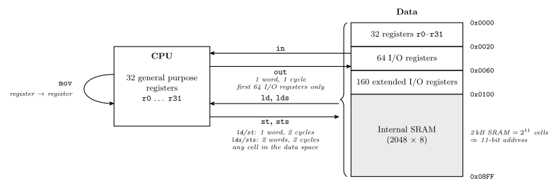
Figure 4: Where data can move. The CPU’s 32 registers are on the left; the data address space is the stack on the right, lowest address at the top. in and out reach only the first 64 I/O registers, one instruction word and one cycle each; ld, st, lds and sts reach any cell of the whole space, which is what the brace marks. The hex boundaries and the SRAM size are from the datasheet memory map in Lecture 11. The 2 kB / \(2^{11}\) cells / 11 bits label sizes the SRAM alone — the stack as a whole runs to 0x08FF.
Figure 4 puts in/out, load/store and data movement in one picture. The register file, the I/O registers and the SRAM are all cells of the same data address space, and the five instructions differ only in which part of it they can reach and how they name it. in/out are the cheap route but stop at I/O register 63. Everything past there has to be reached the long way, by data address, with lds/sts (avr-io-ports).
Dyadic instructions
A dyadic instruction combines 2 operands to produce a result. There are usually two types: arithmetic (ADD r5, r6) and logical, i.e. bitwise (AND r5, r6).
Monadic instructions
A monadic instruction takes one operand and gives one result:
| Operation | Example |
|---|---|
| Setting a register (all 1’s) | SER r16 ≡ ldi r16, 0xFF |
| Clearing a register | CLR r5 |
| Negation (2’s complement) | NEG r5 |
| Inversion (1’s complement negation) | COM r5 |
| Shifting & rotation | the shift and rotate instructions below |
The register numbers differ for a reason: SER r16 but CLR r5. ser expands to ldi, so it inherits the r16–r31 restriction, while clr expands to eor rd, rd and reaches any register (avr-instructions).
Shift instructions
There are three:
- LSL = Logical Shift Left
- LSR = Logical Shift Right
- ASR = Arithmetic Shift Right
They differ in what enters the vacated end and where the departing bit goes. LSL puts 0 into the bottom and sends bit 7 out to C. LSR puts 0 into the top and sends bit 0 out to C. ASR replicates the sign bit into itself and sends bit 0 out to C.
Worked in four bits, as in Figure 5:
| Shift | Worked | Reading |
|---|---|---|
| LSL | 0010 2 → 0100 4 → 1000 8, × 2 each step |
doubling, one place at a time |
| LSR | 1000 (−8) → 0100 4; and 0110 6 ÷2 → 0011 3, unsigned |
halving, unsigned |
| ASR | 1000 (−8) ÷2 → 1100 (−4), the sign bit replicates |
halving, signed |
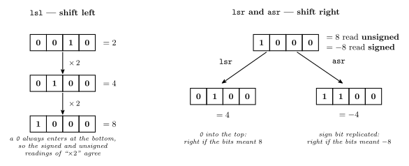
Figure 5: The three shifts worked in four bits for legibility. Left: lsl doubles, 2 → 4 → 8, and a 0 always enters at the bottom so the signed and unsigned readings agree. Right: the same four bits shifted right two ways. 1000 does not say whether it means 8 or \(-8\); the instruction is where that is declared, and each answer is right for one reading and wrong for the other.
The 1000 row is the one that matters. The same four bits are 8 to an unsigned reading and −8 to a signed one. Four bits are used here for legibility; in a real 8-bit register the equivalent pair is 10000000, 128 unsigned and −128 signed. The two shifts give different answers: LSR yields 0100 (4, right for the unsigned reading), ASR yields 1100 (−4, right for the signed one). The instruction is where you declare which interpretation you meant — see binary-number-representations and the reference treatment in avr-instructions.
Rotate instructions
There are two:
- ROL = Rotate Left through Carry
- ROR = Rotate Right through Carry
Each rotate has two halves: the carry goes into the register at the vacated end, and the bit falling out of the other end goes into the carry. A rotate is a shift whose vacated end is fed from C rather than a constant — so the register and the carry flag together behave as a nine-bit ring.
Worked: shifting a 16-bit value
What AVR instruction should follow
lsl r14to perform a multiplication by 2 of the 16-bit unsigned value stored inr13:r14?A.
asl r13, B.lsl r13, C.rol r13or D.rol r14.
C. rol r13. Figure 6 shows why.
    lsl  r14             ; low byte x2; its bit 7 falls out into C
    rol  r13             ; high byte x2, pulling C into its bit 0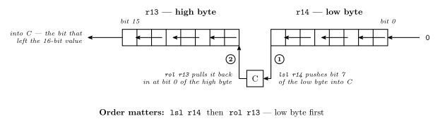
Figure 6: Doubling a 16-bit value in two steps. r13:r14 is one 16-bit value spread over two 8-bit registers, high byte named first. Step 1, lsl r14, shifts the low byte left, feeds a 0 in at bit 0 and pushes its bit 7 out into C. Step 2, rol r13, shifts the high byte left and pulls exactly that bit back in at its bit 0 — which is why rol r13 is the instruction that follows.
The others fail, each differently:
- A.
asl r13and B.lsl r13— the same operation under two names (shifting left, a0always enters), and both feedr13a zero, throwing away the bitr14just produced. - D.
rol r14— the right instruction on the wrong byte.
The general shape: a value wider than the machine is processed low end first, and the carry flag carries between the pieces.
Comparison instructions
A comparison is the same as subtraction, with the result not saved. It sets status register flags (Z, N, C, V …). Equality is what a compare is usually asked, and the flag for that is Z, which is 1 when the two are equal:
cp r5, r6 ; computes r5 - r6, keeps only the flagsThe instruction reference specifies which status register bits are set by which instructions — per instruction, not by one general rule. The table for the instructions met so far is in avr-instructions.
Branch instructions
Branches are based on status register values:
breq label |
Branch if Z = 1 |
brne label |
Branch if Z = 0 |
Compare then branch is the entire conditional. Labels and the program skeleton the branches sit in are in avr-program-structure.
Addressing modes
Instruction operands can come from different places:
| Mode | AVR example | |
|---|---|---|
| Immediate | An operand value is in the instruction | andi r17, 0xBA |
| Register | Only register numbers in instruction | and r18, r19 |
| Direct | Memory address is in the instruction | lds r15, $1234 |
| Indirect | Memory address in register; the register number is in the instruction | ld r5, X |
The direct form occupies two instruction words (32 bits). That is the cost that distinguishes it from indirect, which stays one word.
These addressing mode names are as per Tanenbaum, Structured Computer Organization. The AVR instruction set manual uses different names, so match on the behaviour, not the word. Full treatment in addressing-modes.
4. Data types
Numeric
- Integers of different lengths (8, 16, 32, 64 bits), possibly signed or unsigned
- Floating point numbers, e.g. 32 bits (single precision) or 64 bits (double precision) — \(A = \pi r^2\) with \(3.14\) is the case that forces the type
- Many others
Non-numeric
- Boolean (0 means false, 1 means true) — stored in a whole byte or word
- Bit-map (collection of Booleans, e.g. 8 in a byte)
- Characters
- Pointers (memory addresses)
A Boolean is a bit’s worth of information but costs a whole byte, unless you pack eight of them into one. That is what a bit-map is, and why bit-masking exists as a technique.
Hardware support
Different machines provide hardware support for different data types.
Intel-64 Architecture
| Data type | 8 bits | 16 bits | 32 bits | 64 bits | 128 bits |
|---|---|---|---|---|---|
| Signed integer | ✓ | ✓ | ✓ | ✓ | |
| Unsigned integer | ✓ | ✓ | ✓ | ✓ | |
| BCD integer | ✓ | ||||
| Floating point | ✓ | ✓ |
Atmel AVR
| Data type | 8 bits | 16 bits | 32 bits | 64 bits | 128 bits |
|---|---|---|---|---|---|
| Signed integer | ✓ | ||||
| Unsigned integer | ✓ | ||||
| BCD integer | |||||
| Floating point |
Two ticks against eleven. The AVR supports exactly one data type in hardware: an 8-bit integer, signed or unsigned.
Other data types can be supported through software. For example, 16-bit integer operations can be built out of 8-bit operations, using a sequence of instructions. So the table is a statement about cost, not possibility — nothing in it is unavailable, it just takes more instructions and more cycles.
AVR example of 16-bit addition
Add the 16-bit quantity
r5:r4tor11:r10. (Result should be inr11:r10.)
Two instructions, worked as long addition in Figure 7:
    add  r10, r4         ; r10 <- r10 + r4        (low bytes; carry out lands in C)
    adc  r11, r5         ; r11 <- r11 + r5 + C    (high bytes, plus that carry)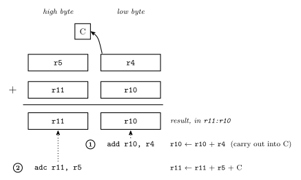
Figure 7: 16-bit addition as long addition with one byte per column, high byte on the left. Step 1, add r10, r4, adds the low column and leaves any carry out of bit 7 in C. Step 2, adc r11, r5, adds the high column and that carry. This is the whole of how an 8-bit machine does 16-bit arithmetic.
ADD on the low bytes leaves any carry out of bit 7 in C; ADC on the high bytes adds it back in. It is column-by-column carrying, exactly as on paper, one byte per column — and nothing may sit between the two instructions that disturbs C.
Summary
| Memory models | Lecture 11 |
| Registers | Lecture 11 |
| Instructions | ✓ |
| Data types | ✓ |
Knowing all these details is enough to write machine code that runs on the CPU and to build the CPU.
See also
- avr-instructions — every instruction here, with encodings and flags
- addressing-modes — the four modes in full
- instruction-set-architecture — the four pillars, and the data type tables
- avr-io-ports · avr-program-structure · bit-masking · binary-number-representations
- 2026-08-31-instruction-set-architecture-part-1 — Lecture 11
- week6-lab-avr-io-ports — Lab 10, which assumes this lecture
Lab 10 — AVR Assembly and the AVR 324 Dev Board
Learning Lab 10, the first lab where a program leaves the simulator and drives real hardware. See avr-io-ports for the ports and registers, avr-program-structure for the template every task is built on, and io-board for the switches, LEDs and buttons being wired up.
What this lab covers
- AVR I/O ports: register numbers; port, pin and data direction registers;
INandOUTinstructions - Using and programming the 324 Dev board
- Assumed knowledge: Lectures 10 and 11, 2026-08-27-avr-introduction and 2026-08-31-instruction-set-architecture-part-1.
inandoutare Lecture 11 material that Lecture 12 repeats.
Admin — dongles. By the end of semester you will be using two USB-A cables for data (one for programming, one for serial communication), one of them from about halfway through the semester. On a personal laptop that may mean a dongle; there are workarounds, but they all have downsides. Get one sooner rather than later. (The same warning as in week5-lab-avr-assembly-one; this is the lab where the cable is first needed.)
From assembly program to chip
A very simplified description of what is happening inside the microcontroller in terms of low-level programming:
\[\text{assembly language program} \longrightarrow \text{machine code} \longrightarrow \text{ATmega324A}\]
The example program
    MOV R3, R5
    ADD R3, R4
    NEG R5
    IN  R3, PINA
    OUT R5, PORTB
assembles to 11010……, 11011……, … which is then downloaded into program memory (Flash — 32 kB). Inside the chip: program memory holding those words, data memory (SRAM — 2 kB), the AVR 8-bit CPU (ALU + CU + Reg), and other components.
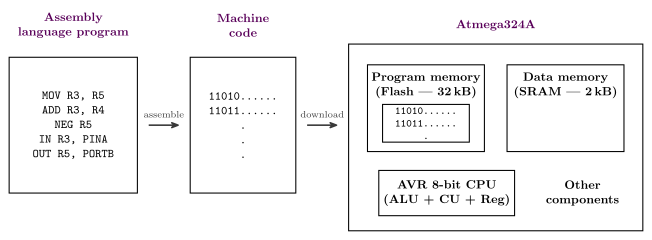
Figure 8: A very simplified picture of what is happening inside the microcontroller. Assembly text becomes machine code becomes the contents of flash; the CPU then reads it back out of flash one word at a time. The chip’s own panel is the point: program memory and data memory are separate blocks with separate address spaces (memory-models), which is why the machine code lands in one of them and the program’s variables in the other.
The last two lines of that program are the new part. Everything before them stays inside the CPU; IN and OUT are how a program reaches the outside world. Full picture in avr-architecture.
AVR I/O registers and general purpose I/O ports
- The ATmega324A has 224 I/O registers, accessible at memory addresses 32 (
0x20) to 255 (0xFF) with theld(load) andst(store) instructions. - The first 64 I/O registers (0 to 63) can also be accessed using
inandout. - Pages 636 to 639 of the datasheet (or the I/O register summary) have the I/O register details.
- Many registers are reserved (not used).
- The general purpose I/O port registers are
DDRA,PORTA,PINA,DDRB,PORTB,PINB, …
Extract from the I/O register list
The bottom of the list is the twelve port registers. The datasheet writes both numbers in one Address column: the I/O register number first, the data memory address in brackets after it.
Address — I/O reg no. (data memory address) |
Name |
|---|---|
0x0B (0x2B) |
PORTD |
0x0A (0x2A) |
DDRD |
0x09 (0x29) |
PIND |
0x08 (0x28) |
PORTC |
0x07 (0x27) |
DDRC |
0x06 (0x26) |
PINC |
0x05 (0x25) |
PORTB |
0x04 (0x24) |
DDRB |
0x03 (0x23) |
PINB |
0x02 (0x22) |
PORTA |
0x01 (0x21) |
DDRA |
0x00 (0x20) |
PINA |
I/O reg number (0–63) — used with
IN/OUT
Data memory address — used withLD/ST
Further up the same table are 0x15 (0x35) TIFR0 through 0x18 (0x38) TIFR3, with 0x14 (0x34) marked Reserved.
Each row also carries the eight bit names for that register — PORTD7 … PORTD0, DDD7 … DDD0, PIND7 … PIND0 — which is where the per-pin names come from. The data-direction bits are DDDn/DDCn/DDBn/DDAn, not DDRDn: the register is DDRD, its bits are DDD7–DDD0.
Two numbers for one register, differing by the 0x20 the general purpose register file occupies at the bottom of the data space. Which number you write depends on which instruction you use, and the two worked questions below both turn on getting that right. See avr-io-ports.
GPIO ports
The datasheet block diagram has PORT A (8), PORT B (8), PORT C (8) and PORT D (8) around the edges of the chip: four 8-bit ports, PA7..0, PB7..0, PD7..0 — and port C as PC5..0 with TOSC1/PC6 and TOSC2/PC7 broken out, since those two pins are shared with the timer oscillator (avr-io-ports).
PIN, PORT and DDR registers
One bit of one port is three D flip-flops, DDRA0, PORTA0 and PINA0, around a tri-state buffer and one microcontroller pin. DDRA0 enables the buffer, PORTA0 supplies what it drives, and PINA0 samples whatever is on the pin. Drawn out and read through in avr-io-ports.
in and out
in rd, P |
Load I/O register value into general purpose register | rd: r0 to r31; P = I/O register number (0 to 63, 0 to 0x3F) or name |
out P, rr |
Store value from general purpose register into I/O register | rr: r0 to r31; P = 0 to 63 (0 to 0x3F) or name |
The “or name” form is covered under Using port names below.
Worked: setting port A to all outputs
Which instructions will set all bits of port A to be outputs?
Answer:
    ldi r16, 0xFF
    out 0x01, r16
From the table above, I/O register 0x01 is DDRA, and a 1 in a direction bit means output, so 0xFF makes all eight pins outputs. Three wrong answers, each one lookup away:
| Changed line | Why not |
|---|---|
out 0x02, r16 |
0x02 is PORTA — this writes an output value, not a direction |
ldi r16, 0x00 |
right register, wrong value — 0x00 makes all eight pins inputs |
out 0x00, r16 |
0x00 is PINA — the read register |
Right and wrong answers are the same two instructions; only the constant and the I/O register number move.
Using port names
Including the m324Adef.inc file lets a program use names for I/O registers rather than numbers:
.include "m324Adef.inc"The contents of this file are included directly in the program. So the answer above can be written without ever looking up a number:
    ldi  r16, 0xFF       ; every direction bit 1 = output
    out  DDRA, r16
Identical machine code — the assembler substitutes 0x01 for DDRA. Write the names; look the numbers up only when reading someone else’s listing or an exam question.
Worked: setting port B to all inputs
Which instructions will set all bits of port B to be inputs?
Answer:
    ldi r16, 0x00
    out DDRB, r16
Two independent things have to be right:
out, notin.inloads from an I/O register into a general purpose one.in DDRB, r16is not a legal instruction at all:in’s destination is written first and must be one of r0–r31, andDDRBis not one of those.in r16, DDRBis legal — it reads the direction register into r16, throwing away the constant just loaded there, and changes nothing.0x00, not0xFF.out DDRB, r16with0xFFin r16 is the correct instruction with the value that makes every pin an output.
Across the two questions, the pair that must line up is (direction register, direction value): 1 is output and 0 is input.
ser and clr instructions
Short-hand ways of setting/clearing all bits of a register:
ser rd (set register) |
exactly the same as ldi rd, 0xFF — only works with registers ≥ 16 |
ser r16 |
clr rd (clear register) |
exactly the same as eor rd, rd |
clr r3 |
So both answers above can drop the constant — one instruction swapped for one, same two-line shape: ser r16 / out DDRA, r16 and clr r16 / out DDRB, r16. The asymmetry in which registers each reaches is not arbitrary — it follows from what they expand to; see avr-instructions.
Labels and the jmp instruction
        jmp RESET
        …
RESET:  …
        …

loop:   …
        …
        jmp loop
AVR assembly language program template
                             ; Comments start with semicolons
.include "m324Adef.inc"
    jmp RESET                ; <- vector table
    ; Interrupt handlers go here
    ; (more on this in week 9/10)

RESET:                       ; Starting point   <- RESET handler
    ...                      ; Initialisation code
                             ; e.g. set DDRs
loop:
    ...                      ; Do stuff        <- main code
    jmp loop                 ; Repeat
Three labelled sections — vector table, RESET handler, main code. Why it has that shape, and why the main body is an infinite loop, is in avr-program-structure.
Connecting the programmer
When attaching the programmer’s ribbon cable to the breadboard:
Red wire on the ground side
Getting this wrong damages hardware. See the Pololu Programmer Guide on Blackboard for the rest.
Tasks
Task 1 — AVR assembly program
Write an AVR program to
- read the value on port A pins
- flip (invert) all the bits
- write the value out to port C
- do this repeatedly
Remember to set data direction registers appropriately before reading/writing values.
Enter the code into Microchip Studio, simulate your code, check that it works by checking the appropriate registers.
Task 2 — Programming the AVR board
Connect 8 switches on the IO Board to AVR port A; and 8 LEDs to AVR port C.
- Use 4-way cables with 4-way headers on each end
- Build and download the program you wrote in task 1
See the Pololu Programmer Guide on Blackboard.
Test your program — change the values on the switches connected to port A and observe the LEDs.
Modify your program to output the two’s complement (negative) of the input, rather than the ones’ complement (inversion). Build, download and test it.
Task Three — Adding inputs
Connect 8 switches on the IO Board to AVR port A; and 8 LEDs to AVR port C; and connect the 4 push buttons on the IO Board to AVR port D (4 least significant bits).
- Use individual jumper wires for this if required
Write an AVR assembly language program to repeatedly
- Read the value on port A pins (8 bits)
- Read the value on port D pins (8 bits)
- Clear the upper nybble (4 bits) of this value (read from the four buttons); consider bitwise AND to do this
Add the two values and output the result to port C.
Make sure you set the data direction registers appropriately.
Build, download and test your program and verify it behaves as expected.
Task Four — Population count
- Count the number of high bits
- Read through
popcount.pdfon BlackBoard - Several variations (extension tasks)
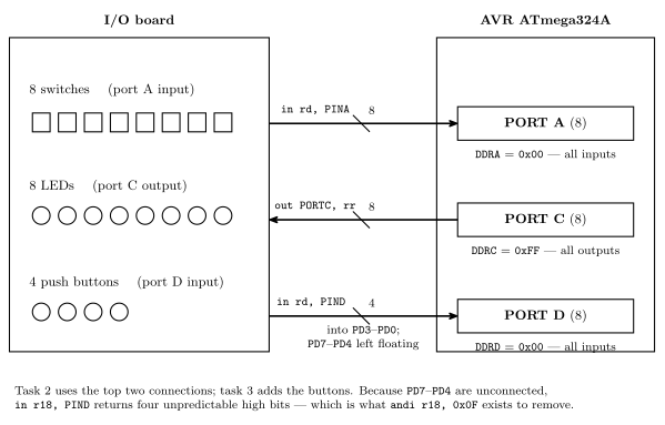
Figure 9: What tasks 2 and 3 ask you to wire, and what each port’s data direction register has to say about it. The direction rule is what fixes each DDR value: 1 is output, 0 is input. The four unconnected port-D pins are the reason task 3 asks for a bitwise AND.
Working — Task 1
The three things the task asks for map one-to-one onto three instructions, and the fourth (“do this repeatedly”) is the jmp at the bottom of the template.
.include "m324Adef.inc"

    jmp RESET

RESET:
    clr  r16
    out  DDRA, r16       ; port A: all inputs  (0 = input)
    ser  r16
    out  DDRC, r16       ; port C: all outputs (1 = output)

loop:
    in   r17, PINA       ; read what is actually on the pins
    com  r17             ; ones' complement - flip every bit
    out  PORTC, r17      ; drive the result out
    jmp  loop
Four things worth being deliberate about:
PINAfor the read,PORTCfor the write. ReadingPORTAwould give back whatever was last written to it, not what the switches are doing; writingPINCwould not drive anything. Input side reads PIN, output side writes PORT — see avr-io-ports.- The direction registers are set once, in
RESET, not inside the loop. They do not change. ser r16needs r16 or above, which is why the scratch register isr16rather than, say,r3.clrwould have been happy either way.comis the inversion the task asks for — ones’ complement, i.e. flip every bit (avr-instructions).
Simulating it, as the task asks: Microchip Studio’s simulator has no switches, so set PINA by hand in the I/O view and single-step; r17 should show the complement and PORTC should follow it.
Working — Task 2
Same program, now on real hardware: 8 switches → port A, 8 LEDs → port C, 4-way cables at both ends. Flip a switch and the corresponding LED should go off — the inversion is visible as switch and LED disagreeing on every bit.
The modification is a one-instruction change:
    in   r17, PINA
    neg  r17             ; two's complement instead of ones'
    out  PORTC, r17
com gives \(\overline{x}\); neg gives \(\overline{x} + 1\), which is the two’s complement negation (binary-number-representations). The two differ by exactly one, so on the LEDs the difference is a single increment — easiest to see with all switches down: com shows 1111 1111, neg shows 0000 0000.
Working — Task 3
Three ports now, and one masking step:
.include "m324Adef.inc"

    jmp RESET

RESET:
    clr  r16
    out  DDRA, r16       ; port A: 8 switches, all inputs
    out  DDRD, r16       ; port D: 4 buttons on the low nybble, all inputs
    ser  r16
    out  DDRC, r16       ; port C: 8 LEDs, all outputs

loop:
    in   r17, PINA       ; the eight switches
    in   r18, PIND       ; the four buttons - in the low nybble
    andi r18, 0x0F       ; clear the upper nybble
    add  r17, r18
    out  PORTC, r17      ; sum to the LEDs
    jmp  loop
Why the mask is needed at all, since only four pins are wired: in r18, PIND reads all eight bits of port D, and the four upper pins have nothing connected to them. An unconnected input pin floats, so those bits are unpredictable — masking them off is what makes the sum depend only on the buttons. andi r18, 0x0F is the extract case of bit-masking: 1s on the bits to keep, 0s on the bits to discard.
andi works here because r18 is a high register. Reading the buttons into a low register instead would need the mask in a register of its own:
    ldi  r19, 0x0F
    and  r5, r19
add r17, r18 writes into r17, since AVR is two-operand (avr-instructions) — so the switch value is consumed by the addition, which is fine, it is re-read at the top of every pass.
What to expect on the board: switches give 0–255, buttons add 0–15, and the sum is 8-bit, so pressing buttons with the switches near 0xFF wraps around. That wrap is the carry being discarded, and it is worth watching for deliberately — it is the same 8-bit-only arithmetic that the 16-bit addition in 2026-09-03-instruction-set-architecture-part-2 exists to work around.
Working — Task 4
popcount.pdf on Blackboard has both the method and the extension variations.
One approach with the instructions met so far: shift the value one bit at a time and count the bits that fall out into C. lsr moves bit 0 into the carry flag (avr-instructions), so eight shifts pass every bit through C in turn, and a conditional add of 1 to a counter each time gives the population count. It needs two things beyond those instructions: a carry-conditional branch and a loop counter.
See also
- avr-io-ports — the I/O registers, the three port registers, and
in/out - avr-program-structure — the template, labels and
jmp - avr-instructions · bit-masking · avr-architecture
- io-board — the switches, LEDs and buttons being wired to the ports
- week5-lab-avr-assembly-one — Lab 9, the simulator-only predecessor
- 2026-08-31-instruction-set-architecture-part-1 · 2026-09-03-instruction-set-architecture-part-2 — Lectures 11 and 12
Reference material
Addressing Modes
Instruction operands can come from different places, and how an instruction says where to find its operand is its addressing mode. It is part of the instruction encoding, so it is part of the ISA (instruction-set-architecture) — see avr-instructions for the instructions named here.
The names below are as per Tanenbaum, Structured Computer Organization. The AVR instruction set manual uses different names for the same ideas, so match on the behaviour rather than the word when reading the datasheet.
The four modes
| Mode | What is in the instruction | Where the operand is | AVR example |
|---|---|---|---|
| Immediate | the operand value itself | in the instruction word | andi r17, 0xBA |
| Register | only register numbers | in a register | and r18, r19 |
| Direct | the memory address | in memory, at that address | lds r15, $1234 |
| Indirect | a register number; that register holds the address | in memory, at the address the register holds | ld r5, X |
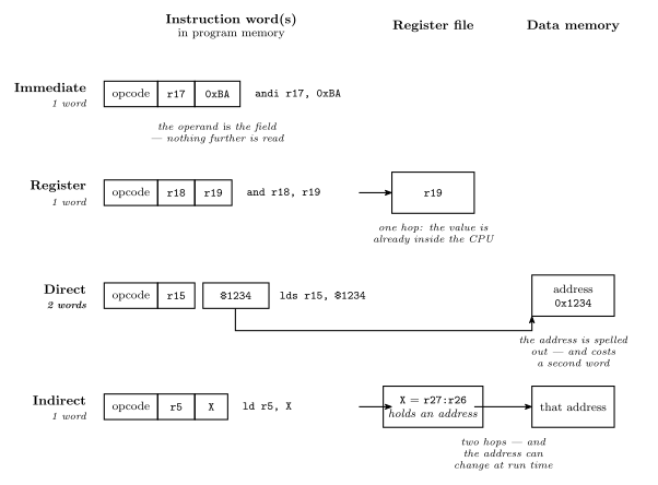
Figure 10: The four modes as one question: how far does the machine have to go to reach the operand? Immediate stops at the instruction itself. Register takes one hop, into the register file. Direct takes one hop into memory, but needs a second instruction word to carry the address. Indirect takes two hops and stays one word, and because its address lives in a register it can change while the program runs. The field splits shown inside the instruction words are schematic, not the real AVR encodings.
Figure 10 is the whole comparison in one line: immediate, register, direct, indirect is a list in increasing order of indirection, and every step down it either costs an instruction word or costs a hop through some storage on the way to the operand.
Immediate addressing
An operand value is in the instruction. andi r17, 0xBA carries 0xBA inside the instruction word itself — nothing is fetched from anywhere, the bits are the number. On AVR the immediate instructions are the ones whose mnemonic ends in i (ldi, andi, ori, cpi) and they pay for the immediate with encoding space: only four bits are left for the register, which is exactly why they reach r16–r31 only.
Register addressing
Only register numbers in the instruction. and r18, r19 names two registers and nothing else; the values are already inside the CPU. This is the cheapest mode there is — no memory access at all — and it is why the AVR is a load/store machine: no arithmetic or logic instruction touches memory, its operands are either registers (and r18, r19) or an immediate carried in the instruction word (andi r17, 0xBA). Anything in SRAM has to be loaded into a register first.
Direct addressing
Memory address is in the instruction. lds r15, $1234 spells the address out in full.
These AVR instructions occupy two instruction words (32 bits): sixteen bits are nowhere near enough for both an opcode and a 16-bit address, so the address gets a word of its own. That is the standing trade — a direct access is simple to read and needs no setup, but it costs double the program memory and cannot be computed at run time.
Indirect addressing
Memory address in register; register number is in the instruction. ld r5, X says “load from wherever X points”, and X is the pointer register pair of avr-architecture.
The instruction stays one word, because it only has to name which pointer. The address itself is data now, not code — which is what makes loops over arrays possible: increment the pointer and the same instruction reaches the next element.
Reading the trade-off
| Instruction words | Address decided | Costs | |
|---|---|---|---|
| Immediate | 1 | when you write the program | encoding space, hence ldi’s r16–r31 limit |
| Register | 1 | — | nothing; the value is already in the CPU |
| Direct | 2 | when you write the program | an extra program-memory word per access |
| Indirect | 1 | at run time | a pointer register, and loading it first |
The pattern: anything the instruction has to say costs instruction bits; anything it can point at costs a register and a setup step instead. Direct and indirect are the same access to the same memory cell — they differ only in which of those two prices you pay.
What the extra word does not cost
ld/st (indirect) are one instruction word, two cycles; lds/sts (direct) are two instruction words, two cycles. So direct addressing’s extra cost is paid entirely in program memory, not in time — both memory forms take the same two cycles, because both make one data-memory access and that access is what dominates.
For contrast, in/out use neither mode — they name an I/O register number directly in the instruction — and take one word, one cycle. That one-cycle figure is the reason in/out exist at all rather than everything going through lds/sts (avr-io-ports).
See also
- instruction-set-architecture — addressing modes as part of the “instructions” pillar
- avr-instructions —
ld/lds/st/stsand the immediate instructions - avr-architecture — the X, Y and Z pointer registers indirect mode uses
- memory-models — the address space being addressed
- 2026-09-03-instruction-set-architecture-part-2 — Lecture 12
AVR Architecture
The Atmel AVR: what is on the chip, how the CPU is laid out, and where the fetch-decode-execute cycle happens in it. See cpu-organisation for the generic picture this specialises and avr-instructions for what it executes.
Microcontroller, not microprocessor
Atmel AVR devices are microcontrollers. A microcontroller includes lots of components on one chip:
- CPU
- Memory (RAM)
- Program memory
- Input/output devices
That is the distinction from a microprocessor, which is the CPU alone. An ATmega324A is not a CPU — it contains a CPU, alongside memory and a large collection of peripherals, so that a useful system can be one chip rather than a board full of them.
The AVR CPU
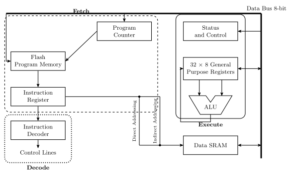
Figure 11: The AVR CPU core, with the three stages of the cycle marked. Fetch (dashed) reads the next instruction from flash under the program counter into the instruction register; decode (dotted) turns it into control lines; execute (solid) runs it over the register file, ALU and status register, with the 8-bit data bus tying everything together. The two lines dropping to the Data SRAM are the direct and indirect addressing routes — both come out of the instruction, which is why they leave from the instruction register. The execute group takes in the status register, the register file and the ALU; the Data SRAM sits outside it.
Reading the diagram as the cycle of fetch-decode-execute-cycle:
| Stage | Blocks involved |
|---|---|
| Fetch | Program Counter → Flash Program Memory → Instruction Register |
| Decode | Instruction Register → Instruction Decoder → Control Lines |
| Execute | General purpose registers → ALU → back to registers, with Status and Control updated |
Because these three groups are largely separate hardware, the AVR overlaps them: while one instruction executes, the next is being fetched. This course calls it a three-stage pipeline. The ATmega164A/324A/644A/1284P datasheet describes the core as “single level pipelining”, i.e. fetch and execute overlapping, which is two stages. Answer three-stage pipeline in the exam, but the datasheet is the authority on the hardware.
The pieces
| Block | Notes |
|---|---|
| Flash program memory | Holds the program. 32 kB on the ATmega324A, and non-volatile — it survives power loss |
| Program Counter | Addresses flash to select the next instruction — the PC of cpu-organisation |
| Instruction Register | Holds the instruction currently being worked on |
| Instruction Decoder | Turns the instruction’s bits into control lines — this is the control unit |
| 32 × 8 general purpose registers | R0–R31, each 8 bits wide, built from flip-flops |
| ALU | 8-bit, so AVR is an 8-bit machine |
| Status and Control | Holds the flags the ALU produces — N, Z, C, V among others |
| Data SRAM | 2 kB, volatile — static RAM, i.e. flip-flops |
| Data bus | 8 bits wide, tying the execute-side blocks together |
Two addressing routes reach the SRAM, drawn as the two vertical paths in Figure 11 — direct addressing (the address is in the instruction) and indirect addressing (the address is in a register). Both leave from the instruction register, because in either case it is the instruction that says which cell is wanted; they differ only in whether it says so with a literal address or with the name of a pointer. Both, and the other two modes, are in addressing-modes.
Four numbers define the chip: the flash is 32 kB and non-volatile; the SRAM is 2 kB, volatile, and made of static flip-flops; the register file is 32 registers, r0…r31, each 8 bits wide and made of flip-flops; and the ALU is 8-bit, which makes the AVR an 8-bit machine.
The register file
General purpose registers (0–31) are quite regular and can be used interchangeably. Two exceptions are worth having by heart:
- A few instructions work on half the registers (r16–r31), because only 4 bits are used to represent the operand in the instruction and \(2^4 = 16\).
LDI,SER,ANDI,ORIandCPIare among them — see avr-instructions. - X, Y and Z are register pairs that double as 16-bit pointers.
X, Y and Z
The top six registers of the file are those three pairs, low byte in the lower-numbered register:
| Pointer | High : Low | Register addresses |
|---|---|---|
| X | R27 : R26 | 0x1B : 0x1A |
| Y | R29 : R28 | 0x1D : 0x1C |
| Z | R31 : R30 | 0x1F : 0x1E |
Two 8-bit registers side by side make a 16-bit address — which is what the data space needs and no single 8-bit register can hold. They are what indirect addressing uses: ld r5, X means “load from wherever X points”, and the instruction only has to name which pointer, so it stays one word (addressing-modes).
The low byte living in the lower-numbered register is the same little-endian convention the AVR uses in memory (memory-models).
Address spaces
The AVR is a Harvard machine — separate address spaces for instructions and data — so 0x0000 names two entirely different locations depending on which space is meant, and the instruction decides.
Data address space — 0x0000 to 0x08FF
| Region | Addresses | Size |
|---|---|---|
| 32 Registers | 0x0000–0x001F |
32 |
| 64 I/O Registers | 0x0020–0x005F |
64 |
| 160 Ext I/O Reg. | 0x0060–0x00FF |
160 |
| Internal SRAM | 0x0100–0x08FF |
2048 bytes (2 kB) |
The register file and all 224 I/O registers are mapped into the data space, ahead of the SRAM. That is what lets lds/sts reach an I/O register by its data address while in/out reach the first 64 by their I/O register number — the two numbering systems differ by exactly the 0x20 the register file occupies. Details in avr-io-ports.
The datasheet draws the SRAM box as 1024/2048/4096/16384 × 8 because the diagram covers the whole ATmega164A/324A/644A/1284P family; the 324A is the 2048 entry, which is what puts the top of the data space at 0x08FF.
Program memory — 0x0000 to 0x3FFF
\(2^{14}\) 16-bit words: 16,384 instruction words = 32,768 bytes = 32 kB. The datasheet splits it into an Application Flash Section and, at the highest addresses, a Boot Flash Section.
0x3FFF \(= 2^{14} - 1\), and the sizing arithmetic — why 32 kB of program memory is 14 address bits rather than 15 — is worked through in memory-models. The short version: the cells are 16 bits wide, so there are half as many of them as there are bytes.
The AVR status register
8 bits, all readable and writable, all reset to 0:
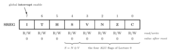
Figure 12: The status register, in the three-row form the datasheet uses: bit numbers above, flag names in the boxes, then the access row and the value each bit takes after reset. The callout names bit 7, the global interrupt enable; the braces underneath mark the four ALU flags and the sign flag \(S = N \oplus V\).
Instruction descriptions refer to these as SREG(n) by bit number:
| Flag | Bit | Meaning |
|---|---|---|
| C | SREG(0) | carry — was a carry out generated? |
| Z | SREG(1) | zero — was the result 0? |
| N | SREG(2) | negative — the sign bit of the result |
| V | SREG(3) | overflow — did a two’s complement addition/subtraction overflow? |
| S | SREG(4) | sign, \(= N \oplus V\) — the sign of the result corrected for any overflow |
| H | SREG(5) | half-carry — carry out of bit 3 |
| T | SREG(6) | transfer bit, used by BLD and BST |
| I | SREG(7) | global interrupt enable — set by sei, cleared by cli; cleared by the hardware when it takes an interrupt and set again by reti (avr-interrupts) |
C, Z, N and V are exactly the four flags of fetch-decode-execute-cycle.
S is not simply “the sign bit” — that is N. \(S = N \oplus V\) means: the result is negative (with no overflow), or would have been negative had overflow not occurred. That correction is what makes signed comparisons work, which is why the signed branches (BRLT, BRGE) test S while the unsigned ones (BRLO, BRSH) test C. The four cases — including the overflow case where N alone gives the wrong answer — are drawn in 2026-09-14-flow-of-control, and the branch pairs are tabulated in avr-branches-and-jumps.
The one-line meanings and the SREG(n) numbering are those of Atmel’s AVR Instruction Set Manual and the instruction summary in the ATmega324A datasheet. The I/O register map is the I/O register summary, pages 636–639 of the ATmega164A/324A/644A/1284P datasheet, which writes the I/O register number first and the data memory address in parentheses after it.
On-chip peripherals (ATmega324A)
Beyond the CPU and its memories, the chip carries a large set of peripherals — this is what makes it a microcontroller rather than a processor. The two figures nest: the whole of Figure 11 is what sits inside the single box marked AVR CPU in Figure 13.
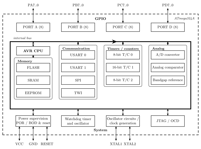
Figure 13: What is on the ATmega324A: the datasheet block diagram, rearranged into clusters by kind of thing — GPIO, memory, communication, timers/counters, analog and system. The dashed outline is the package boundary and the heavy rectangle inside it the internal bus, both as the datasheet draws them; the individual peripheral-to-port wiring is left out.
| Group | On the chip |
|---|---|
| General purpose I/O | PORT A, PORT B, PORT C, PORT D — four 8-bit ports |
| Communication | USART 0, USART 1, SPI, TWI |
| Timers/counters | 8-bit T/C 0, 16-bit T/C 1, 8-bit T/C 2 (T/C 3 is on the ATmega1284/1284P, not the 324A — the family datasheet’s block diagram covers both) |
| Analog | A/D converter, analog comparator, internal bandgap reference |
| Memory | Flash (program), SRAM (data), EEPROM (data, non-volatile) |
| System | Power supervision (POR/BOD & reset), watchdog timer and oscillator, oscillator/clock generation (XTAL1, XTAL2), JTAG/OCD |
There are three memories with three different jobs: flash for the program, SRAM for volatile working data, and EEPROM for data that must survive a power cycle. SRAM and EEPROM are the pair to keep straight: both hold data, and they differ only in surviving a power cycle.
See also
- cpu-organisation · fetch-decode-execute-cycle · instruction-set-architecture
- avr-instructions — the instruction set this hardware runs
- avr-io-ports — the I/O registers and the four GPIO ports
- avr-interrupts — the I bit, the vector table and the peripherals’ interrupt sources
- avr-timers-and-counters · avr-usart · avr-spi · analog-to-digital-conversion — four of the peripherals in detail
- memory-models · addressing-modes — the two address spaces, and how instructions name them
- assembly-process — flash, SRAM and EEPROM as the assembler’s three segments
- memory-technologies — flash, SRAM and EEPROM as technologies, and what the boot loader section is for · memory-hierarchy-and-cache — where the registers and SRAM sit by speed, and why the AVR needs no cache
- binary-number-representations — the flags’ two’s complement interpretation
- 2026-08-27-avr-introduction — Lecture 10
- 2026-08-31-instruction-set-architecture-part-1 — Lecture 11
AVR Branches and Jumps
How an AVR program’s control leaves the straight line: the ten conditional branches and which status flag each one reads, why greater than needs two different instructions for signed and unsigned bytes, the three unconditional jumps and how far each can reach, and the assembly idioms — if, if … else, counted and conditional loops — built from them. First met in 2026-09-14-flow-of-control, with the compare instructions and breq/brne first met in 2026-09-03-instruction-set-architecture-part-2. Procedure calls, the other way control moves, are in procedures-and-the-stack.
Flow of control
The flow of control is the sequence in which instructions actually execute. By default it is linear: every fetch-decode-execute cycle ends with \(PC \leftarrow PC + 1\) (fetch-decode-execute-cycle), so the next instruction is the next one in memory. Four kinds of instruction replace that increment with a new value:
| Decides | ||
|---|---|---|
| Branches | conditional | a status-register flag |
| Jumps | unconditional | nothing — always taken |
| Procedure calls and returns | unconditional, and they remember where they came from | procedures-and-the-stack |
| Interrupts / traps | triggered by hardware, not by an instruction | polling-and-interrupts · avr-interrupts |
Everything below is one instruction that writes the PC.
Conditional branches
A conditional branch tests one bit of the status register (avr-architecture) and, if the bit has the value the instruction wants, loads the PC with the address of a label; otherwise execution falls through to the next instruction. There is one instruction per flag per value:
| Branch if flag = | C | N | V | S = N ⊕ V | Z | T | H | I |
|---|---|---|---|---|---|---|---|---|
| 0 | brsh (= brcc) |
brpl |
brvc |
brge |
brne |
brtc |
brhc |
brid |
| 1 | brlo (= brcs) |
brmi |
brvs |
brlt |
breq |
brts |
brhs |
brie |
The first five columns are the ten branches counted above; the last three are the same pattern applied to the remaining flags and are in the instruction set reference. The mnemonics read as the condition, not the flag: brsh is branch if same or higher and happens to be branch if carry clear; brge is branch if greater or equal and happens to be branch if S clear. Learn them as conditions and the flags take care of themselves.
Every branch is relative and short. The offset is seven bits, so a conditional branch can reach only about 64 words either side of itself. For a farther target, branch on the opposite condition around a jmp:
    cp   r5, r6
    brne skip          ; opposite of the condition wanted
    jmp  far_away      ; taken only when r5 == r6
skip:
A taken branch costs two cycles, a not-taken one; the branch itself is one 16-bit word.
Setting the flags first
A branch reads flags; something has to have written them. Usually that is a compare (avr-instructions):
| Computes | Keeps | |
|---|---|---|
cp rd, rr |
rd − rr |
flags only |
cpi rd, K |
rd − K |
flags only — rd must be r16–r31 |
tst rd |
rd AND rd |
flags only — Z and N say whether rd is zero or negative |
but any ALU instruction sets flags, and a branch straight after an add, sub, dec or andi tests the result of that. dec r17 followed by brne loop is the standard loop counter, and no cp is needed. The rule from avr-program-structure holds either way: nothing that disturbs the flag may sit between the setter and the branch.
Signed and unsigned comparisons
Equality is the same question for signed and unsigned bytes, so breq and brne serve both. Ordering is not: whether 1111 1111 is bigger than 0000 0001 depends on whether it means 255 or −1, and the bits alone cannot say (binary-number-representations). The cp sets the same flags either way; the programmer chooses which pair of branches to read them with, and thereby declares the type:
Branch if rd ≥ rr |
Branch if rd < rr |
Reads | |
|---|---|---|---|
| unsigned | brsh — same or higher |
brlo — lower |
C: an unsigned subtraction needs a borrow exactly when the result went below zero |
| signed | brge — greater or equal |
brlt — less than |
S = N ⊕ V: the sign of the result, corrected for overflow |
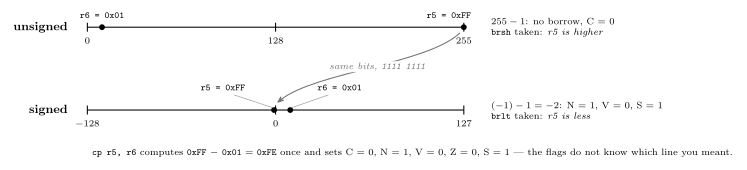
Figure 14: The same two bit patterns on the two number lines an 8-bit register can be read against. As unsigned values, 0xFF is 255 and sits at the far right, above 0x01; as two’s complement values it is \(-1\) and sits just left of zero, below 0x01. One cp r5, r6 produces one set of flags for both readings. The unsigned branches take their answer from the carry flag, which records whether the subtraction had to borrow; the signed branches take theirs from S, which is the sign of the difference with any overflow undone. Choosing brsh or brlt after the compare is the only place the program says which line it meant.
Why S and not N. N is the top bit of the 8-bit result. When a signed subtraction overflows — a large positive minus a large negative, say — the true difference does not fit in 8 bits, the stored result wraps, and its top bit is the opposite of the true sign. V is set in exactly that case. So \(S = N \oplus V\) is the true sign whether or not overflow happened, and one flag test decides < correctly across the whole range; the four cases are drawn in 2026-09-14-flow-of-control. In C none of this is visible: the compiler reads the variable’s declared type and emits brlo for unsigned char and brlt for char, the same way it picks lsr or asr for >> (c-operators).
Unconditional jumps
| Instruction | Target | Size | Cycles | Reach |
|---|---|---|---|---|
jmp label |
absolute address | 32-bit (two words) | 3 | anywhere in program memory |
rjmp label |
PC + signed offset | 16-bit | 2 | ±2 K words (12-bit offset, −2048 to +2047) |
ijmp |
the address held in Z | 16-bit | 2 | anywhere; the target is a run-time value |
jmp carries a full program-memory address — 14 bits for the ATmega324A’s 16 K words of flash — which does not fit beside an opcode in one 16-bit word, so it takes two words and an extra cycle. rjmp carries a 12-bit offset from the instruction’s own position in one word, one cycle less, and reaches ±2 K words; in a program of a few hundred instructions every jump is within range, and it is the normal choice. ijmp takes the destination from Z, the pointer register of addressing-modes, so a program can compute where to go — a jump table, or C’s switch. The assembler resolves labels to addresses or offsets for all three; the programmer writes the label.
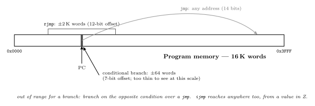
Figure 15: How far each kind of jump can reach from the instruction executing it. Program memory is the ATmega324A’s 16,K words; the marker is the current PC. A conditional branch carries a 7-bit offset and reaches about 64 words either way, an rjmp carries a 12-bit offset and reaches 2,K words either way, and a jmp carries the whole 14-bit address and reaches anywhere. The three are drawn to scale against the memory: the branch window is a sliver, the rjmp window covers a quarter of the chip, and the labs’ programs never leave either. The narrower the reach, the shorter and faster the instruction.
The idioms
Every C control structure (c-control-flow) compiles to a handful of these shapes. The branch is always on the opposite of the source condition, because what the branch does is skip the body.
if:
    cp   r5, r6
    brlt endif         ; skip the body when r5 < r6 (signed)
    ...                ; body: runs when r5 >= r6
endif:
if … else — the else part is the code the branch does not skip, and it needs a jmp past the if part:
    cp   r5, r6
    brge then
    ...                ; else part
    rjmp endif
then:
    ...                ; if part
endif:
while — test at the top, jump back at the bottom:
loop:
    cp   r5, r6
    brsh done          ; exit when r5 >= r6 (unsigned)
    ...                ; body
    rjmp loop
done:
Counted loop — count down to zero so the decrement sets Z for free:
    ldi  r17, 10       ; ten times
loop:
    ...                ; body
    dec  r17           ; sets Z when r17 reaches 0
    brne loop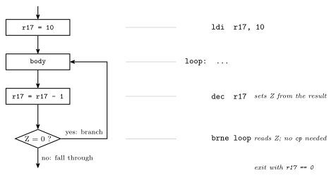
Figure 16: A counted loop, as a flowchart and as the four instructions that implement it. The counter is loaded once; the body runs; the decrement both updates the counter and sets the zero flag from the result; brne reads that flag and either returns to the label or falls out. Counting down rather than up saves the compare: dec leaves Z = 1 exactly when the counter has reached zero, so the branch tests the arithmetic directly. The body executes ten times, with r17 holding 10 down to 1 inside it and 0 on exit — the assembly form of for (i = 10; i != 0; i--).
Picking the branch. Write the C condition, decide signed or unsigned, and take the opposite instruction from the table:
| Source condition | Unsigned: skip with | Signed: skip with |
|---|---|---|
a == b |
brne |
brne |
a != b |
breq |
breq |
a < b |
brsh |
brge |
a >= b |
brlo |
brlt |
a > b |
swap operands: cp b, a then brsh |
cp b, a then brge |
a <= b |
cp b, a then brlo |
cp b, a then brlt |
There is no greater than branch; a > b is b < a, so compare the other way round.
See also
- avr-program-structure — labels, the template, and compare-then-branch drawn out
- procedures-and-the-stack —
call,rcall,icallandret: the jumps that come back - polling-and-interrupts — the fourth way the PC leaves its sequence, with no instruction asking
- avr-instructions —
cp,cpi,tst,dec, and which flags each instruction sets - avr-architecture — the status register; \(S = N \oplus V\)
- c-control-flow — the same shapes in C · binary-number-representations — signed and unsigned bytes
- assembly-process — how the assembler gives a label its address, counting each
jmpas two words - 2026-09-14-flow-of-control — Lecture 15 · 2026-09-03-instruction-set-architecture-part-2 — Lecture 12
AVR Instructions
The AVR instructions introduced so far, in assembly and in machine code. See instruction-set-architecture for what an instruction set is and avr-architecture for the hardware that runs these.
The full alphabetical instruction set — each mnemonic with its operation, description, flags affected, clock count, opcode pattern and an example — is in the AVR instruction set reference: Atmel’s AVR Instruction Set Manual, and the instruction summary in the ATmega324A datasheet the course says to keep open. The notation key immediately below and the per-instruction flag table at the end are unverified against that reference — check them against your own copy before leaning on them.
Reading the instruction set reference
Operand notation — how an operand’s allowed values map onto opcode bits:
| Notation | Meaning | Values | Opcode pattern |
|---|---|---|---|
Rd |
destination register (may be a source too) | r0…r31 | ddddd |
| r16…r31 | dddd (register number − 16) |
||
Rr |
source register | r0…r31 | rrrrr |
Rh:Rl |
register pair as a 16-bit quantity | r25:r24 / X / Y / Z | dd (00 / 01 / 10 / 11) |
K |
constant data | 0…255 | KKKKKKKK |
k |
constant address | −64…63, −2048…2047, 0…65535 | kkkkkkk … kkkk kkkk kkkk kkkk |
b |
bit number in a register | 0…7 | bbb |
s |
bit in the status register | 0…7 | sss |
P |
I/O register number | 0…63 | PPPPPP |
q |
displacement for direct addressing | 0…63 | qqqqqq |
The Rd row is the whole story behind LDI’s restriction — an instruction spending five bits on the register gets all 32; one spending four gets sixteen, and pays for it by starting at r16.
Operation notation — used in the Operation column:
M[a] / PM[a] / IO[a] |
SRAM cell / program memory (flash) byte / I/O register at address a |
PC / SP / STACK |
program counter / stack pointer / M[SP] |
← |
assigned value |
reg(a) |
bit a of register reg, numbered 7…0 most to least significant |
Flag names in the Flags Affected column are the SREG bits of avr-architecture.
Register conventions
Two operand names recur throughout the instruction set:
rd— the destination register.rr— the source register.
AVR is a two-operand machine: the destination is also one of the sources, so add rd, rr means rd ← rd + rr. (Contrast a three-operand ISA such as ARM, where add rd, r1, r2 leaves both sources untouched.) This matters when reading code — an AVR arithmetic instruction always overwrites one of its inputs.
Instructions by type
The instruction set can be cut two ways.
By what the instruction touches — the instruction-type list of instruction-set-architecture, filled in with the instructions so far:
| Type | Does | AVR so far |
|---|---|---|
| Input/Output | communicate with I/O devices/ports | IN, OUT |
| Load/Store | move data from/to memory | LD, LDS, ST, STS |
| Move | copy data between registers | MOV |
| Arithmetic | addition, subtraction, … | ADD, ADC, SUB, INC, NEG |
| Logical | Boolean operations | AND, ANDI, OR, ORI, EOR, COM |
| Branching | deciding which instruction to perform next | JMP, BREQ, BRNE |
By operand count, which splits the arithmetic and logical group instead:
| AVR examples | ||
|---|---|---|
| Dyadic | combine 2 operands to produce a result | add r5, r6 (arithmetic) · and r5, r6 (logical, bitwise) |
| Monadic | one operand → one result | ser r16 (set) · clr r5 (clear) · neg r5 (2’s complement) · com r5 (1’s complement) · the shifts and rotates |
The second cut is the one that predicts the syntax: a dyadic instruction has a comma in it, a monadic one does not.
The instructions so far
| Instruction | Meaning | Example |
|---|---|---|
MOV rd, rr |
copy contents of rr into rd — rd ← rr |
mov r3, r14 |
ADD rd, rr |
add contents of rr to rd — rd ← rd + rr |
add r5, r6 |
ADC rd, rr |
add with carry — rd ← rd + rr + C |
adc r11, r5 |
AND rd, rr |
bitwise AND, result into rd |
|
OR rd, rr |
bitwise OR, result into rd |
|
EOR rd, rr |
bitwise exclusive-OR, result into rd |
|
INC rd |
rd ← rd + 1 |
inc r22 |
LDI rd, number |
load immediate — put the number into rd |
ldi r16, 73 |
SER rd |
set all bits — rd ← $FF. Same as ldi rd, 0xFF, so r16–r31 only |
ser r17 |
CLR rd |
clear all bits — rd ← 0. Same as eor rd, rd, so any register |
clr r3 |
SUB rd, rr |
rd ← rd − rr |
sub r7, r19 |
COM rd |
one’s complement — flip all bits | com r8 |
NEG rd |
two’s complement — negate | neg r9 |
ANDI rd, K |
bitwise AND with a constant — r16–r31 only | andi r16, 0x01 |
ORI rd, K |
bitwise OR with a constant — r16–r31 only | ori r16, 0xF0 |
MOV is named misleadingly: it copies, it does not move. The source register is unchanged. It also affects no flags, which is what makes it safe to shuffle values between operations without disturbing the status register.
SER and CLR are short-hand ways of setting/clearing all bits of a register, and their restrictions differ because their expansions do:
| Exactly the same as | Reaches | |
|---|---|---|
ser rd (set register) |
ldi rd, 0xFF |
r16–r31 only — it inherits LDI’s four-bit register field |
clr rd (clear register) |
eor rd, rd |
any register, r0–r31 — EOR is a two-register instruction with five bits for each |
So clr r3 is legal and ser r3 is not, which looks arbitrary until you look at what each one assembles to. clr is also the reason \(X \oplus X = 0\) from bit-masking is worth remembering: XORing a register with itself is how the machine zeroes one.
Compare instructions
These do the arithmetic, discard the result, and keep only the flags — which is exactly what a conditional branch needs.
| Instruction | Does | Note |
|---|---|---|
CP rd, rr |
rd − rr |
compares two registers |
CPI rd, K |
rd − K |
compares against a constant — like ldi, r16–r31 only |
TST rd |
rd AND rd |
examines one register; literally the same operation as and rd, rd |
tst looks odd until you notice that ANDing a value with itself leaves it unchanged (\(X \cdot X = X\)) but still sets N and Z from it — so it is a zero/sign test that costs nothing and clobbers nothing. See bit-masking.
A comparison is the same as subtraction, with the result not saved — it exists only to set status register flags (Z, N, C, V …). And the instruction reference specifies which status register bits are set by which instructions: the flags are defined per instruction rather than falling out of one shared adder, which is the point of the table at the end of this note.
Branch instructions
Based on status register values — the flags a compare just set:
Branches to label if |
|
|---|---|
BREQ label |
Z = 1 |
BRNE label |
Z = 0 |
Together with CP that is a complete conditional: compare, which sets Z exactly when the two operands were equal, then branch on Z.
    cp   r5, r6          ; r5 - r6, result thrown away, flags kept
    breq same            ; Z = 1, i.e. r5 == r6
JMP label is the unconditional version — it tests nothing and always goes. Labels, and the program skeleton the branches live in, are in avr-program-structure.
breq/brne are two of ten: there is one branch per status flag per value, and the pairs that matter for ordering are brsh/brlo (unsigned, on C) and brge/brlt (signed, on S) — the full table, and why the signed pair reads S rather than N, are in avr-branches-and-jumps.
Control flow
The instructions that write the PC, and the two stack instructions that go with the calls (avr-branches-and-jumps, procedures-and-the-stack):
| Instruction | Does | Words | Cycles |
|---|---|---|---|
BRxx label |
branch if a flag has the wanted value; reach ±64 words | 1 | 1 (not taken) / 2 (taken) |
JMP label |
PC ← address of label |
2 | 3 |
RJMP label |
PC ← PC + offset; reach ±2 K words | 1 | 2 |
IJMP |
PC ← Z | 1 | 2 |
CALL label |
push the return address, then as JMP |
2 | 4 |
RCALL label |
push the return address, then as RJMP |
1 | 3 |
ICALL |
push the return address, then as IJMP |
1 | 3 |
RET |
pop the return address into PC | 1 | 4 |
PUSH rr |
store rr at SP, SP ← SP − 1 |
1 | 2 |
POP rd |
SP ← SP + 1, load rd from SP |
1 | 2 |
None of these touches the status register except by what the pushed and popped values happen to be; a call between a cp and its branch is safe only if the procedure preserves the flags, which in practice means it is not.
Three more belong to interrupts, and between them they are the only instructions that change the I bit (avr-interrupts):
| Instruction | Does | Words | Cycles |
|---|---|---|---|
SEI |
I ← 1: interrupts enabled | 1 | 1 |
CLI |
I ← 0: interrupts disabled | 1 | 1 |
RETI |
pop the return address into PC, and I ← 1 | 1 | 4 |
RETI is RET plus set I. A handler that ends in RET returns to the right place and leaves interrupts off for good.
Data movement
Data is usually copied, not moved — in every instruction below the source is left alone. What changes is where the two ends are:
| Direction | Called | AVR |
|---|---|---|
| register → register | move | mov |
| memory → register | load | lds, ld |
| register → memory | store | sts, st |
| I/O register → register | input | in |
| register → I/O register | output | out |
Three different places a value can live — a general purpose register, data memory, an I/O register — and a different instruction family for each. The one thing that is genuinely out of reach is SRAM from in/out: P only goes up to 0x3F, so those two never leave the first 64 I/O registers.
Everything else is a question of cost and numbering, not reachability. Because the I/O registers are mapped into the data space (avr-io-ports), lds/sts can reach one — in r16, 0x09 and lds r16, 0x29 both read PIND, the second for two instruction words instead of one. The bug to actually watch for is writing the I/O register number where the data address belongs, or the reverse.
Load and store
| Does | Addressing | Words | Cycles | |
|---|---|---|---|---|
LD rd, X |
rd ← Mem[X] |
indirect — address in the pointer register | 1 | 2 |
ST X, rr |
Mem[X] ← rr |
indirect | 1 | 2 |
LDS rd, k |
rd ← Mem[k] |
direct — 16-bit address in the instruction | 2 (32 bits) | 2 |
STS k, rr |
Mem[k] ← rr |
direct | 2 | 2 |
For example:
    ld   r5, X           ; r5 <- Mem[X]
    st   X, r5           ; Mem[X] <- r5
    lds  r5, 0x20        ; r5 <- Mem[0x20]
    sts  0x20, r5        ; Mem[0x20] <- r5
Both pairs reach the same data space — the difference is only where the address comes from (addressing-modes), and lds/sts pay a second instruction word for spelling it out. X here is the pointer pair of avr-architecture.
In and out
| Does | Words | Cycles | |
|---|---|---|---|
IN rd, P |
rd ← I/O register P |
1 | 1 |
OUT P, rr |
I/O register P ← rr |
1 | 1 |
rd/rr may be any of r0–r31 — unlike ldi, these are not restricted to the top half — and P is an I/O register number 0–63 (0x00–0x3F) or a name from m324Adef.inc. Examples: in r5, 0x26 (I/O register 0x26 is TCNT0) and out PORTD, r6. Full treatment in avr-io-ports.
One word and one cycle makes these the cheapest access on the chip — cheaper than reaching the very same register through lds/sts, which is the whole reason the first 64 I/O registers are special.
Shifts and rotates
Monadic instructions that move every bit one place. They differ only in what arrives at the vacated end and what happens to the bit that falls off — and in all five, the bit that falls off lands in C.
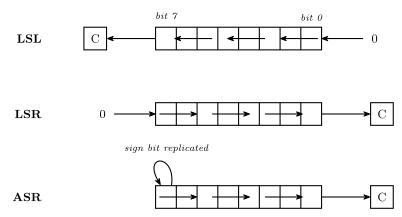
Figure 17: The three shift instructions. LSL and LSR feed a 0 into the vacated end; ASR feeds the sign bit back into itself, which is what makes it a signed division. In all three the bit shifted out lands in the carry flag.
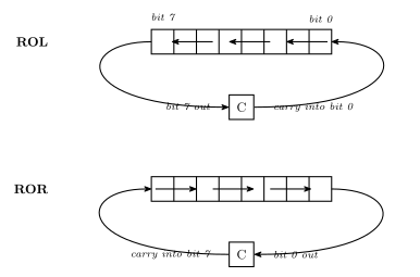
Figure 18: The two rotate instructions. A rotate is a shift whose vacated end is fed from the carry flag instead of a constant, so the register and C together behave as a nine-bit ring.
| Name | Into the vacated end | Out | |
|---|---|---|---|
LSL rd |
Logical Shift Left | 0 → bit 0 |
bit 7 → C |
LSR rd |
Logical Shift Right | 0 → bit 7 |
bit 0 → C |
ASR rd |
Arithmetic Shift Right | bit 7 replicated into itself | bit 0 → C |
ROL rd |
ROtate Left through carry | C → bit 0 | bit 7 → C |
ROR rd |
ROtate Right through carry | C → bit 7 | bit 0 → C |
What they compute
Shifting a binary number one place is multiplying or dividing it by two, which is the whole reason these exist. Using four bits for legibility:
| Worked example | ||
|---|---|---|
LSL |
× 2 | 0010 (2) → 0100 (4) → 1000 (8) |
LSR |
÷ 2, read unsigned | 0110 (6) → 0011 (3); 1000 (8 unsigned) → 0100 (4) |
ASR |
÷ 2, read signed | 1000 (\(-8\)) → 1100 (\(-4\)) |
LSR and ASR are the pair to keep straight. Given 1000, LSR produces 0100 — right if the value meant unsigned 8, wrong if it meant \(-8\). ASR replicates the sign bit into the vacated position and produces 1100 \(= -4\). The same bits go in; the instruction is where you declare which interpretation you meant (binary-number-representations).
There is no matching pair going the other way, because left shifts need no such distinction: a 0 always enters at the bottom, and the signed and unsigned readings of “× 2” agree — right up until the result stops fitting in eight bits.
Shifting a value wider than eight bits
Rotates exist to carry a bit from one byte into the next. To multiply the 16-bit unsigned value in r13:r14 by two (so r13 is the high byte, r14 the low):
    lsl  r14             ; low byte x2; bit 7 falls out into C
    rol  r13             ; high byte x2, pulling C into its bit 0
LSL on the low byte pushes its top bit into C; ROL on the high byte pulls exactly that bit back in at the bottom. The two instructions together shift a sixteen-bit quantity one place.
The wrong answers are worth naming, because each fails differently. lsl r13 (and asl r13, which is the same operation under another name — shifting left, a 0 always enters) shifts the high byte but feeds it a 0, discarding the bit the low byte just produced. rol r14 rotates the wrong byte.
Building wider operations from 8-bit ones
The AVR supports exactly one data type in hardware — an 8-bit integer (instruction-set-architecture). Everything wider is a sequence of instructions, and C is what stitches the pieces together.
Add the 16-bit quantity r5:r4 to r11:r10, result in r11:r10 — high byte named first, so r4 and r10 are the low bytes:
    add  r10, r4         ; r10 <- r10 + r4        (low bytes; carry out lands in C)
    adc  r11, r5         ; r11 <- r11 + r5 + C    (high bytes, plus that carry)
ADD on the low bytes leaves any carry out of bit 7 in C, and ADC on the high bytes adds it back in — the same column-by-column carrying as long addition on paper, one byte per column.
The order is not negotiable, and neither is what sits between the two lines: adc has to run after the add that produced the carry, and any instruction in between that touches C ruins the result. That is the general shape of multi-byte arithmetic on an 8-bit machine — low end first, and nothing allowed to disturb the flag in the middle.
Constants
Constants do not have to be hexadecimal. All five of these load the same value into r17:
| Written | Radix | |
|---|---|---|
ldi r17, 0x34 |
hexadecimal | 0x prefix |
ldi r17, $34 |
hexadecimal | $ prefix |
ldi r17, 52 |
decimal | no prefix |
ldi r17, 064 |
octal | a leading 0 |
ldi r17, 0b00110100 |
binary | 0b prefix |
\(\texttt{0x34} = 52 = 64_8 = \texttt{0b00110100}\). The octal form is the trap: a leading zero changes the radix, so 012 is 10, not 12.
LDI’s restrictions
LDI is the one with strings attached:
- Registers r16 to r31 only. Not r0–r15.
- 8-bit numbers,
00000000to11111111. Written in decimal the range is \(-128\) to \(255\) — that span covers both the signed and the unsigned reading of eight bits.
A counter-example, and the legal version of it:
    ldi  r0, 5           ; NOT legal - r0 is below r16
    ldi  r16, 5          ; the same idea, in a register ldi can reach
The register restriction is not arbitrary: it falls straight out of the encoding below, which has only four bits for the register number.
Machine code
Each instruction is a 16-bit word made of an opcode and operand bit fields — see instruction-set-architecture. In the AVR datasheet’s notation, a format like 0000 11rd dddd rrrr means the literal bits are fixed and each letter is one bit of an operand, gathered from wherever it appears.
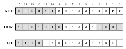
Figure 19: Three AVR instruction encodings, each 16 bits. Fixed opcode bits are shaded; letters are operand bits. In ADD and LDI the operand bits are not contiguous — the register number’s top bit sits apart from the rest, and LDI’s constant is split into two nibbles either side of the register field.
ADD — 0000 11rd dddd rrrr
The opcode is bits 15–10, 0000 11 — six fixed bits, all that is left once the two five-bit register numbers have taken ten of the sixteen. The destination register number is d dddd — five bits, so all 32 registers — and the source is r rrrr. Both have their top bit separated from the other four, and note the order in the middle nibble: the source’s top bit (r, bit 9) comes before the destination’s (d, bit 8), even though the mnemonic writes the destination first.
Worked example: add r23, r7.
| Register | In binary (5 bits) | Split as | |
|---|---|---|---|
rd |
r23 = 16 + 4 + 2 + 1 | 10111 |
d = 1, dddd = 0111 |
rr |
r7 = 4 + 2 + 1 | 00111 |
r = 0, rrrr = 0111 |
Dropping those into 0000 11rd dddd rrrr:
\[\texttt{0000 1101 0111 0111}\]
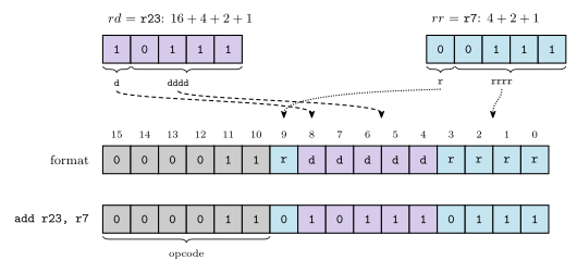
Figure 20: Assembling add r23, r7. Each register number is written as five bits, then torn in two: the top bit goes into the middle nibble and the low four into their own field. Shading, not position, is what tells the two operands apart here. The two guide lines cross because the destination’s bit sits between the source’s two pieces.
COM — 1001 010d dddd 0000
Flip all bits — one’s complement. One register operand, again as d dddd.
Worked example: com r19. r19 = 16 + 2 + 1 = 10011, so d = 1 and dddd = 0011:
\[\texttt{1001 0101 0011 0000}\]
LDI — 1110 KKKK dddd KKKK
Two operand fields:
K— the 8-bit constant, split into two nibbles: the high four bits in the firstKKKKfield, the low four in the last.d— the register number minus 16.
That subtraction is why LDI only reaches r16–r31: the field is four bits, so it can express \(2^4 = 16\) distinct registers, and the ISA spends them on the top half of the register file.
Applying the rule to ldi r16, 73: \(d = 16 - 16 = 0\), so dddd = 0000; \(73 = \texttt{0100 1001}\), so the high nibble is 0100 and the low nibble 1001:
\[\texttt{1110 0100 0000 1001}\]
Flags, by instruction
The reference’s Flags Affected column is worth reading rather than assuming — the flags are defined per instruction, not derived from a single adder. For the instructions above:
| Instruction | Z | C | N | V |
|---|---|---|---|---|
MOV, LDI, SER |
— | — | — | — |
AND, ANDI, OR, ORI, EOR, TST |
from result | unchanged | from result | cleared to 0 |
ADD, ADC, SUB, CP, CPI |
from result | from carry/borrow | from result | signed overflow |
CLR |
always 1 | unchanged | always 0 | cleared to 0 |
COM |
from result | always set to 1 | from result | cleared to 0 |
NEG |
from result | set unless the result is $00 |
from result | set only if the result is $80 |
Two of these will catch you out. The logical operations leave C alone entirely — whatever it held before an and it still holds after. And COM sets C unconditionally, which is not a carry out of anything; it is a defined convention, chosen so that com followed by an increment behaves like a negation.
The CLR row is just the logical row with a result that is guaranteed to be 0x00 — clr rd is eor rd, rd — which makes it the one instruction whose flags you can predict without knowing the operand.
For the shift, rotate and branch instructions, look the flags up in the reference rather than guessing. The one part that is visible in the diagrams above is C: every shift and rotate sets it from the bit that fell out. The rest is defined per instruction, as the paragraph opening this section warns.
For ADD specifically, the manual gives the flags as Boolean formulas over the operand and result bits, writing \(R\) for the result (which equals Rd after the operation):
\[N = R_7 \qquad Z = \overline{R_7}\cdot\overline{R_6}\cdot\overline{R_5}\cdot\overline{R_4}\cdot\overline{R_3}\cdot\overline{R_2}\cdot\overline{R_1}\cdot\overline{R_0}\] \[V = Rd_7 \cdot Rr_7 \cdot \overline{R_7} + \overline{Rd_7}\cdot\overline{Rr_7}\cdot R_7 \qquad C = Rd_7 \cdot Rr_7 + Rr_7 \cdot \overline{R_7} + \overline{R_7}\cdot Rd_7\]
\(Z\) is a NOR over every result bit. \(V\) says overflow happened exactly when both operands had the same sign and the result’s differs — two negatives giving a positive, or two positives giving a negative. And \(S = N \oplus V\), for signed tests. See avr-architecture.
See also
- instruction-set-architecture · avr-architecture · bit-masking
- avr-io-ports — the I/O registers
in/outreach - addressing-modes — the four ways an operand names its value
- avr-program-structure — labels,
jmpand the program skeleton - avr-interrupts —
sei,cli,reti, and which flags an interrupt handler must save - binary-number-representations — one’s and two’s complement, and the \(-128\) to \(255\) range
- 2026-08-27-avr-introduction — Lecture 10
- 2026-09-03-instruction-set-architecture-part-2 — Lecture 12
AVR I/O Ports
How an AVR program actually reads a switch and lights an LED: the I/O register file, the three registers behind every port, the two instructions that reach them, how to change one bit of a port without disturbing the others, what writing to PINx really does, and the pins’ alternate uses by the serial interfaces. See avr-architecture for the chip these live on, avr-instructions for the instruction set, and io-board for the devices that get wired to the pins.
I/O registers
The ATmega324A has 224 I/O registers — registers that control the peripherals and carry data to and from them:
- Timers and counters
- Analog to digital converters
- Serial input/output
- General purpose input/output ports
They are not the general purpose registers. Some instructions work with these, others with r0–r31, and confusing the two is the standard beginner error — ldi r16, 0xFF and out DDRA, r16 name completely different register files with the same-looking numbers.
Some addresses are reserved (not actually available on this device). The full list is the I/O register summary, pages 636 to 639 of the datasheet.
Where they live, and how you get at them
I/O registers 0 to 223 sit in the data address space at memory addresses 32 to 255 (0x20 to 0xFF) — see memory-models for why the AVR has a separate data space at all. That gives two ways to name the same register, and two names for it:
| Range | Reached by | |
|---|---|---|
| First 64 I/O registers (0 to 63) | data addresses 0x20–0x5F |
in and out and ld/st |
| Other 160 — the “extended” I/O registers (64 to 223) | data addresses 0x60–0xFF |
ld/st only |
so the two numbering systems differ by a constant:
\[\text{data memory address} = \text{I/O register number} + \texttt{0x20}\]
The offset is exactly the 32 general purpose registers, which occupy 0x0000–0x001F at the bottom of the data space ahead of them.
Why the split exists at all: in/out encode the I/O register number in six bits of the instruction word, and \(2^6 = 64\). Everything past register 63 has no room in the encoding, so it can only be reached the long way round, by its data address.
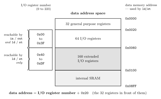
Figure 21: The bottom of the ATmega324A data address space, and the two numbering systems that live on it. Every I/O register has two numbers — its I/O register number (what in/out take) and its data memory address (what ld/st take) — and they differ by a constant 0x20, because the 32 general purpose registers sit in front of them in the same space. Only the first 64 I/O registers have an I/O register number small enough to fit the six operand bits of in/out; the 160 extended ones can be reached by their data address alone. The map follows the convention of csse2010-diagram-notation: lowest address at the top, hex addresses outside.
Extract from the I/O register list
The general purpose port registers are the first twelve entries, in the order PIN, DDR, PORT for each port in turn:
| Data address | I/O reg number | Name |
|---|---|---|
0x2B |
0x0B |
PORTD |
0x2A |
0x0A |
DDRD |
0x29 |
0x09 |
PIND |
0x28 |
0x08 |
PORTC |
0x27 |
0x07 |
DDRC |
0x26 |
0x06 |
PINC |
0x25 |
0x05 |
PORTB |
0x24 |
0x04 |
DDRB |
0x23 |
0x03 |
PINB |
0x22 |
0x02 |
PORTA |
0x21 |
0x01 |
DDRA |
0x20 |
0x00 |
PINA |
Further up the same list, to show the pattern continues and that reserved entries are real:
| Data address | I/O reg number | Name |
|---|---|---|
0x38 |
0x18 |
TIFR3 |
0x37 |
0x17 |
TIFR2 |
0x36 |
0x16 |
TIFR1 |
0x35 |
0x15 |
TIFR0 |
0x34 |
0x14 |
Reserved |
Read the two columns carefully in an exam question. out 0x02, r16 writes PORTA, but sts 0x02, r16 writes general purpose register r2 — the same number, two address spaces, and only the instruction tells them apart.
GPIO ports
The ATmega324A has four 8-bit general purpose I/O ports — PORT A, PORT B, PORT C, PORT D — appearing on the datasheet block diagram as PA7..0, PB7..0, PD7..0 around the edge of the chip, with port C drawn as PC5..0 plus TOSC1/PC6 and TOSC2/PC7 broken out separately — those two pins double as the timer oscillator connections. They are still port C bits, and DDRC/PORTC/PINC still cover all eight.
Three registers are associated with each (x = A, B, C or D):
| Register | Name | What it holds |
|---|---|---|
| DDRx | Data Direction Register | which pins are outputs |
| PORTx | values to output | |
| PINx | values on the pins |
Each is 8 bits — one bit per pin. DDRA0, PORTA0 and PINA0 are the three bits belonging to pin PA0.
What one bit of a port looks like
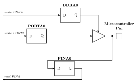
Figure 22: One bit of an AVR port — the three flip-flops behind pin PA0. DDRA0 enables the tri-state buffer, so it decides whether PORTA0’s value is driven onto the pin or the pin is left free for something outside to drive. PINA0 samples whatever is on the pin either way. Hence: DDR is direction, PORT is what you write, PIN is what you read.
1 means output, 0 means input. Writing 0xFF to DDRA makes every bit of port A an output, and writing 0x00 to DDRB makes every bit of port B an input.
Three consequences fall straight out of the circuit:
- PORTx does nothing on a pin whose DDRx bit is 0. The buffer is off; the value sits in the flip-flop unused. (On real AVR hardware it switches an internal pull-up instead.)
- PINx is always live. It samples the pin whether the pin is being driven from inside or outside, so reading PINx on an output pin reads back what you are driving.
- Reading PORTx is not reading the pin. It gives you the value you last wrote. To find out what is there, read PINx — which is why every input example uses
in rd, PINxand neverin rd, PORTx.
in and out
The two instructions that reach the first 64 I/O registers:
| Does | Operands | |
|---|---|---|
in rd, P |
Load I/O register value into general purpose register | rd: r0 to r31. P = I/O register number (0 to 63, 0x00 to 0x3F) or name |
out P, rr |
Store value from general purpose register into I/O register | rr: r0 to r31. P = 0 to 63 (0x00 to 0x3F) or name |
The operand order flips between them, and it flips for a consistent reason: like every AVR instruction, the destination is written first. So the I/O register is the second operand of in and the first of out.
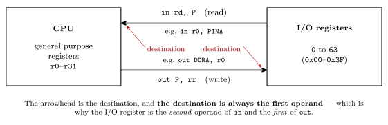
Figure 23: in and out between the two register files: the CPU’s general purpose registers r0–r31 and the first 64 I/O registers. in reads from an I/O register into a general purpose register, out writes the other way, and the head of each arrow, marked destination, is the operand written first. That is why the I/O register is the second operand of in and the first of out.
Answers of the form in DDRB, r16 are the standard trap. What is wrong with them is the mnemonic, not the direction: in’s destination is always one of r0–r31, so it can never be DDRB. Moving a general purpose register into an I/O register is exactly what out does — which is why the right answer in that shape is out DDRB, r16.
in and out reach all 32 general purpose registers, r0–r31 — unlike ldi, they are not restricted to the top half.
Both are one instruction word and one clock cycle, which makes them the cheapest way to touch a peripheral.
Three equivalences, all of them just the number/name table above:
| Written with a number | Same instruction, written with a name |
|---|---|
in r0, 0 |
in r0, PINA |
out 1, r0 |
out DDRA, r0 |
in r5, 0x26 |
in r5, TCNT0 — I/O register 0x26 is timer/counter 0 |
Using port names
Numbers are how the machine sees it; names are how you should write it:
.include "m324Adef.inc"The contents of this file are included directly in the program, and it defines the names for the I/O registers — so DDRA, PORTA, PINA, TCNT0 and the rest can be written instead of 0x01, 0x02, 0x00, 0x26. Everything about the generated machine code is identical; the assembler substitutes the number.
Setting port A (all bits) to be an output, which is the shape of nearly every initialisation block:
    ldi  r16, 0xFF       ; every bit 1 = output
    out  DDRA, r16       ; ... into the direction register
or, using the shorthand of avr-instructions, ser r16 in place of the ldi. Setting a port to be all inputs is the same two lines with 0x00 (or clr), and a mixed port is any other constant — DDRA is a bit pattern like everything else, so ldi r16, 0x0F gives four outputs and four inputs.
Changing one bit of a port
Writing a whole port register is right at initialisation. Afterwards a program usually wants to change one pin and leave the other seven alone, because the other pins belong to other parts of the program. In C that is a read-modify-write with a one-bit mask, the bit named rather than given as a number (bit-masking):
DDRC  |= (1<<5);          /* PC5 becomes an output     */
PORTC |= (1<<5);          /* PC5 driven high           */
PORTC &= ~(1<<5);         /* PC5 driven low            */
PORTC ^= (1<<5);          /* PC5 flipped               */
if (PINC & (1<<2)) { }    /* is PC2 high?              */
In assembly there are two ways:
| Register | Set or clear one bit | |
|---|---|---|
I/O registers 0 to 31, which includes every PINx, DDRx and PORTx |
sbi PORTC, 5 and cbi PORTC, 5 |
one instruction, other bits untouched |
any register in/out reach, 0 to 63 |
in r16, TCCR0B, then ori or andi with the mask, then out TCCR0B, r16 |
three instructions, and a spare register |
sbi and cbi hold the register number in five bits of the instruction, so they reach only the first 32 I/O registers. TCCR0B is I/O register 0x25, 37, which is past them: the long way is the only way. The extended registers past 63, such as TIMSK2 and TCCR1B, need lds and sts in place of in and out.
Writing to PINx
PINx is the port’s input register: reading it gives the levels on the pins. Writing to it is not storing a value. On the ATmega324A, writing a 1 to a bit of PINx toggles the matching bit of PORTx, whatever the pin’s direction, and writing a 0 does nothing.
That makes PINx a quick way to flip a pin:
PINC = (1<<0); /* toggle PC0; the 0s written to the other bits do nothing */and in assembly sbi PINC, 0 does the same in one instruction.
It also makes PINx the wrong register for a clear or a set. PINC &= ~(1<<5) does not clear PC5. If the compiler turns it into a single cbi PINC, 5, it writes a 0 to bit 5 of PINC and nothing happens. If it does a read, an AND and a write, it writes 1s to every other bit that read high, and those pins flip:
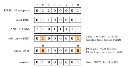
Figure 24: Why a read-modify-write on PINC goes wrong. Port C is all outputs, driving 0110 0001, so its pins read the same. PINC &= ~(1<<5) reads them, clears bit 5 of the reading and writes the result to PINC. A 1 written to a PINx bit is an order to toggle that bit of PORTx, not a value to keep, and a 0 does nothing. So the two other 1s, shaded, flip PC6 and PC0 low, and PC5, the bit meant to be cleared, stays high. The bottom row is what PORTC &= ~(1<<5) would have given.
So: set and clear through PORTx, read through PINx, and write PINx only to toggle.
Alternate pin functions
Most pins have a second job. When the peripheral that owns a pin is switched on, it takes the pin over from the port, and for some pins it overrides DDRx too. The serial interfaces use these:
| Port pin | Package pin | Alternate use | Peripheral |
|---|---|---|---|
| PB0 | 1 | XCK0 | USART0’s clock, used when it is an SPI master |
| PB4 | 5 | \(\overline{\text{SS}}\) | SPI (avr-spi) |
| PB5 | 6 | MOSI | SPI |
| PB6 | 7 | MISO | SPI |
| PB7 | 8 | SCK | SPI |
| PC0 | 22 | SCL | TWI |
| PC1 | 23 | SDA | TWI |
| PD0 | 14 | RXD0 | USART0 (avr-usart) |
| PD1 | 15 | TXD0 | USART0 |
| PD2 | 16 | RXD1 | USART1 |
| PD3 | 17 | TXD1 | USART1 |
| PD4 | 18 | XCK1 | USART1’s clock, used when it is an SPI master |
So the SPI port is the upper half of port B, and the TWI is the bottom two bits of port C. Other pins carry timer outputs, the external interrupts (INT0 and INT1 share PD2 and PD3 with USART1) and, on port A, the analog inputs. A pin can do only one job at a time, so a program that uses the SPI cannot also use PB4 to PB7 as general purpose I/O. The whole pinout is drawn in 2026-10-05-more-io.
Common mistakes
in DDRB, r16.inalways writes a general purpose register. Writing an I/O register isout DDRB, r16.- Reading
PORTxto find out what is on a pin. That gives back what was last written. The pins arePINx. - Setting or clearing a bit through
PINx. A 1 written there toggles, soPINC &= ~(1<<5)flips other pins and leaves PC5 alone. PORTC = (1<<5)to set one pin.=writes all eight bits and drives the other seven low. Use|=.sbiorcbion a register past 31, such asTCCR0B. They cannot reach it; usein,ori/andi,out.- Using a pin as general I/O while its peripheral is on. The SPI, the TWI and the USARTs take their pins over.
See also
- avr-architecture — the data address space these sit in, and the rest of the chip
- avr-instructions · avr-program-structure · bit-masking
- memory-models — why the I/O registers have two addresses
- io-board · device-pinouts — the switches, LEDs and buttons wired to the pins
- week6-lab-avr-io-ports — Lab 10, where this gets wired up
- avr-usart — PD0 and PD1 as a serial port · analog-to-digital-conversion — port A as analog inputs
- avr-spi — PB4 to PB7 as the SPI port · serial-communication — the TWI on PC0 and PC1
- 2026-08-31-instruction-set-architecture-part-1 — Lecture 11 · 2026-10-05-more-io — Lecture 19
AVR Assembly Program Structure
The skeleton every AVR assembly program in this course is built on — what goes at the top, where execution starts, and why it ends in an infinite loop. See avr-instructions for what fills it in and avr-io-ports for what the initialisation section usually does.
The template
                             ; Comments start with semicolons
.include "m324Adef.inc"

    jmp RESET                ; <- vector table
    ; Interrupt handlers go here
    ; (more on this in week 9/10)

RESET:                       ; Starting point   <- RESET handler
    ...                      ; Initialisation code
                             ; e.g. set DDRs

loop:                        ; <- main code
    ...                      ; Do stuff
    jmp loop                 ; Repeat
Three sections, and each is there for a reason:
| Section | What it is |
|---|---|
| Vector table | jmp RESET, then the interrupt handlers |
| RESET handler | the starting point — initialisation code, e.g. setting the data direction registers |
| Main code | the work, ending in a jump back to its own label |
Why the vector table comes first
The chip begins executing at program address 0x0000 — the top of the program memory map in memory-models — and the addresses immediately after it are reserved for interrupt vectors, one per interrupt source. So the very first instruction has to jump over them to reach the real start of the program. That is all jmp RESET is doing.
Everything between that jump and the RESET: label is the vector table itself. It stays empty (comments only) in a program that uses no interrupts — but the jmp has to be there from the first program, because without it execution would fall straight into whatever occupied the vector slots. Once a program does use an interrupt, each vector slot it needs holds a jmp to that source’s handler at a fixed address, placed with .org; the table, the handlers and how to enable them are in avr-interrupts.
Labels and jmp
A label is a name for a position in the program:
        jmp RESET
        …
RESET:  …
        …

loop:   …
        …
        jmp loop
The assembler replaces each label with the program-memory address it ended up at, so jmp loop becomes a jump to a real address. Two properties matter in practice:
- A label is written at the start of the line, ending in a colon; the instruction it names can be on the same line or the next one.
- Labels let you write code without ever computing an address by hand, which is most of what an assembler buys you over machine code (instruction-set-architecture).
jmp RESET at the top of the template needs the address of a label the assembler has not reached yet. It copes by reading the file twice: the first pass only works out where every label lands, using each line’s size, and the second fills the addresses into the instructions (assembly-process). In the template RESET is the address straight after the vector table, worked out the same way.
jmp itself is unconditional. For jumping only sometimes, the branch instructions below take a label in exactly the same way.
Conditional control flow
A branch instruction takes a label just as jmp does, but jumps only if a status register bit says so — so a decision is always written as two instructions, one that sets the flags and one that reads them:
breq label |
branch if Z = 1 |
brne label |
branch if Z = 0 |
The usual flag-setter is cp, which is a subtraction whose result is not saved: it computes rd - rr purely to set Z, N, C, V and the rest, so cp r5, r6 followed by breq branches exactly when the two registers were equal. The instruction reference specifies which status register bits are set by which instructions, per instruction rather than by one general rule — so a compare is not always needed, because whatever ran last may already have set Z. avr-instructions tabulates which does what.
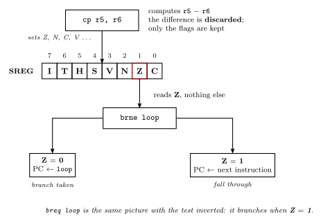
Figure 25: Compare-then-branch: the whole of an AVR conditional. cp performs the subtraction and throws the difference away, keeping only what it did to the flags; brne then reads exactly one of them and either loads the label’s address into the program counter or lets execution fall through to the next instruction. The flag names and their order are those of the AVR status register; the outline on Z marks the one flag brne tests.
Figure 25 is worth reading as the reason labels matter. The branch does not encode “go back three instructions” in a form you have to count out by hand; it names a label, and the assembler works out the address — the same service it performs for jmp RESET at the top of the file.
Two consequences for the template above. First, a loop that should sometimes end is still written as a label plus a branch, not as a special construct: the body falls through when the condition fails. Second, nothing may sit between the flag-setter and the branch that disturbs the flag being tested — the status register is a single shared piece of state, and the instruction in between will happily overwrite it.
The two branches above are the equality pair. The other eight — including the signed and unsigned less than pairs that a loop bound usually needs — and the loop idioms built from them are in avr-branches-and-jumps.
When the program calls procedures
The template above has no stack, because nothing in it calls anything. The moment a program uses call or rcall — or push — the stack pointer must be set first, and it goes at the top of RESET:, before any of the other initialisation:
RESET:
    ldi  r16, low(RAMEND)
    out  SPL, r16
    ldi  r16, high(RAMEND)
    out  SPH, r16
    ...                      ; then set DDRs and the rest as before
RAMEND is the last SRAM address, 0x08FF; the stack starts there and grows downward. Why it has to, and what call and ret do with it, is procedures-and-the-stack. A C program gets these four instructions for free from the compiler’s start-up code.
Variables and constants
The template holds only code. Variables and tables of constants go in the other segments (assembly-process), chosen by .dseg and .cseg:
.include "m324Adef.inc"
.def    temp = r16              ; a name for a register

        .dseg                   ; SRAM: space only
count:  .byte 1                 ; one byte, at 0x0100

        .cseg                   ; flash: code and constants
        jmp  RESET              ; vector table
RESET:
        ldi  temp, low(RAMEND)  ; stack pointer, if anything is called
        out  SPL, temp
        ldi  temp, high(RAMEND)
        out  SPH, temp
        ...                     ; initialisation
loop:
        ...                     ; main code
        jmp  loop

digits: .db  63, 6, 91, 79, 102, 109, 125, 7, 127, 111   ; seven-segment patterns, 0 to 9
Three rules come with it:
- A variable is a label on a
.bytein the data segment. It gets an address,0x0100for the first one, but no value. The program has to store something there, withsts count, tempfor example, before reading it. - Constants go in the code segment, out of the path of execution. The CPU runs whatever is in program memory at the PC, so a table in the middle of the code would be executed as if it were instructions. After the main loop’s
jmp loopis safe, because execution never gets there. Betweenjmp RESETandRESET:is safe for the same reason, but only in a program that uses no interrupts, because that is where the interrupt vectors go.digitsis ten bytes, an even number, so it fills five words with no pad (assembly-process). - A constant is read with
lpm, at its byte address, the label times 2, in Z (memory-models).
Why it ends in an infinite loop
loop: … jmp loop is not a placeholder. A microcontroller program has nowhere to return to — there is no operating system underneath it, and the CPU keeps fetching whatever comes next for as long as it has power. So the main body of an AVR program is a loop that never exits, and “do this repeatedly”, which is how nearly every lab task is worded, is the normal shape rather than a special case.
The division of labour that follows: anything that should happen once goes in the RESET handler (setting DDRs, loading constants), and anything that should happen forever goes in the loop (reading inputs, computing, writing outputs).
See also
- avr-branches-and-jumps — the full branch table, jumps, and the
if/loop idioms · procedures-and-the-stack —call,retand the stack - avr-interrupts — what goes in the vector table, and the handlers after it
- avr-instructions · avr-io-ports · avr-architecture
- assembly-process — statement fields, directives, segments and the two-pass assembler · instruction-set-architecture — assembly, the assembler and the toolchain
- memory-models — the program address space the vector table sits at the bottom of · memory-technologies — flash and SRAM, the memories behind
.csegand.dseg - week6-lab-avr-io-ports — Lab 10, where the template is first used
- 2026-10-08-assembly-process — Lecture 20: how the assembler turns the template into machine code
Binary Number Representations
Bits, bytes, and words
- Bit = binary digit (0 or 1).
- Nibble = 4 bits. It is the unit that makes hexadecimal convenient (one hex digit = one nibble).
- Byte = 8 bits, e.g.
01010111. - Modern computers deal with words, usually a power-of-2 number of bytes: 1, 2, 4, or 8 bytes = 8, 16, 32, 64 bits. The AVR used in this course is at the small end — an 8-bit (1-byte) word; modern CPUs sit at the other end, 32- or 64-bit.
Representing whole (unsigned) numbers
Each bit position has a value — a power of 2, increasing from right (least significant) to left (most significant). Binary → decimal: add the values of each position where the bit is 1.
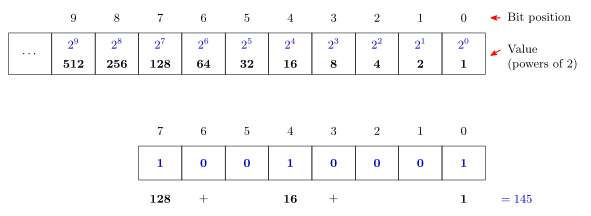
Figure 26: Place values for an unsigned binary number, and a worked conversion. Position \(i\) is worth \(2^i\), so reading a binary number is just adding the place values of the positions holding a 1: \(10010001_2 = 128 + 16 + 1 = 145\).
Most and least significant bits
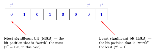
Figure 27: The two ends of a word get names, because almost every later convention (shifting, sign bits, bit numbering in AVR registers) is stated in terms of them. For an \(n\)-bit unsigned word the MSB is worth \(2^{n-1}\) — here \(2^7 = 128\) — and the LSB is always worth \(2^0 = 1\).
Converting decimal to binary
Two equivalent methods, both worked on the same number, 53.
Method 1 — sum of powers of 2. Rewrite \(n\) as a sum of powers of 2, by repeatedly subtracting the largest power of 2 not greater than \(n\) (\(53 - 32 = 21\), \(21 - 16 = 5\), \(5 - 4 = 1\), \(1 - 1 = 0\)). Then assemble the binary number from 1’s in the bit positions corresponding to those powers of 2, and 0’s everywhere else.
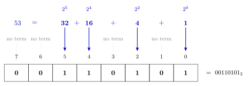
Figure 28: Method 1 on \(53\). Each power of two in the decomposition names one bit position — \(2^5\) is position 5, \(2^4\) is position 4, and so on — and every position with no term in the sum gets a 0. Reading the row off left to right gives \(00110101_2\).
Method 2 — repeated division. Build the bits up from the right (least significant): divide \(n\) by 2, the remainder (0 or 1) is the next bit, then repeat with \(n\) = the quotient. Stop when the quotient reaches 0, and read the remainders upwards.
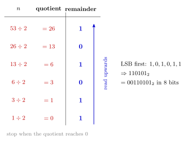
Figure 29: Method 2 on \(53\). The remainders come out LSB-first, which is why the answer has to be read back up the column: \(110101_2\), or \(00110101_2\) padded to a byte. The same procedure with a divisor of 16 or 8 converts to hexadecimal or octal instead.
Number range (unsigned)
- Smallest representable value: all 0’s → 0.
- Largest representable value: all 1’s → for an \(n\)-bit word, \(2^n - 1\) (e.g. 255 for 8 bits).
The \(-1\) is the part worth understanding: an \(n\)-bit word has \(2^n\) distinct patterns, but one of them is spent on zero.
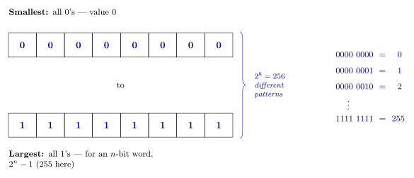
Figure 30: Why the largest unsigned value is \(2^n-1\) and not \(2^n\). Counting up from all-zeros steps through every pattern in turn — each extra bit doubles how many there are, so 8 bits give \(2^8 = 256\) patterns — and because the count starts at 0, the last one is 255.
Other radices
Radix = number system base. A radix-\(k\) number system has \(k\) distinct symbols for digits \(0\) to \(k-1\), and the value of each digit (from the right) is \(k^0, k^1, k^2, \dots\) — so a radix-\(k\) number \(d_{m}\dots d_1 d_0\) is worth \(\sum_i d_i k^i\). E.g. \(1\mathrm{A}_{16} = 1 \cdot 16^1 + 10 \cdot 16^0 = 16 + 10 = 26\).
- Octal (radix-8): symbols
0–7. One octal digit corresponds to exactly 3 bits. - Hexadecimal (radix-16): symbols
0–9,A–F. One hex digit corresponds to exactly 4 bits — very convenient for grouping binary.
| Dec | 0 | 1 | 2 | 3 | 4 | 5 | 6 | 7 | 8 | 9 | 10 | 11 | 12 | 13 | 14 | 15 | 16 | 17 |
|---|---|---|---|---|---|---|---|---|---|---|---|---|---|---|---|---|---|---|
| Oct | 0 | 1 | 2 | 3 | 4 | 5 | 6 | 7 | 10 | 11 | 12 | 13 | 14 | 15 | 16 | 17 | 20 | 21 |
| Hex | 0 | 1 | 2 | 3 | 4 | 5 | 6 | 7 | 8 | 9 | A | B | C | D | E | F | 10 | 11 |
Converting binary ↔︎ hex/octal by grouping
Because \(16 = 2^4\) and \(8 = 2^3\), no arithmetic is needed: group the bits from the right — four at a time for hex, three at a time for octal — and translate each group with the table above. Pad the leftmost group with leading zeros.
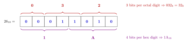
Figure 31: One bit pattern read two ways. Grouping \(00011010_2\) into nibbles from the right gives \(1\) and \(\mathrm{A}\), i.e. \(1\mathrm{A}_{16}\); grouping the same bits in threes gives \(0\), \(3\) and \(2\), i.e. \(32_{8}\). The grouping must start at the right — starting at the left gives the wrong answer whenever the width is not a multiple of 3 or 4.
The same trick read backwards is why hex is used for bit patterns at all: a full byte of 1’s, 1111 1111, is F F = \(\mathtt{0xFF}\) = 255, and any byte can be written as two hex digits.
To convert decimal → any radix, use Method 2 with that radix as the divisor: \(26 \div 16\) gives quotient 1 remainder 10 (= A), so \(26_{10} = 1\mathrm{A}_{16}\); \(26 \div 8\) gives quotient 3 remainder 2, so \(26_{10} = 32_8\). See 2026-07-27-course-intro-bits-bytes-binary for that worked exercise.
Radix notation conventions
Since a bare number like 101 or 747 is ambiguous, a radix indicator is needed. A subscript works generically (e.g. \(101_2\), \(101_{16}\)); in code/assembly, conventions vary. Bolded rows are the ones this course mostly uses:
| Radix | Convention | Example | Where used |
|---|---|---|---|
| any | subscript | \(101_2\), \(101_{16}\) | generic/mathematical |
| Hex | leading 0x |
0x101 |
C, Atmel AVR |
| Hex | trailing h |
101h |
some assembly languages |
| Hex | leading $ |
$747 |
Atmel AVR assembly |
| Octal | leading 0 |
0101 |
C, Atmel AVR |
| Octal | trailing q |
101q |
some assembly languages |
| Octal | leading @ |
@747 |
some assembly languages |
| Binary | leading 0b |
0b101 |
Atmel AVR assembly, some C |
| Binary | trailing b |
101b |
some assembly languages |
| Binary | leading % |
%101 |
some assembly languages |
The octal convention is the trap: in C, a leading 0 silently changes the radix, so 0101 is \(65_{10}\), not \(101_{10}\).
Representing signed numbers
Computers don’t store \(+\) and \(-\) signs; the sign has to be encoded in the bits themselves. Four formats have been used, and all four — plus unsigned — represent positive numbers identically. Only the negatives differ.
Signed magnitude
The leftmost bit is a sign bit (0 positive, 1 negative) and contributes nothing to the magnitude. Negate by inverting the sign bit alone.
Ones’ complement
The sign bit now also carries weight: its position value is \(-(2^{N-1}-1)\). Negate by inverting all the bits.
Two’s complement
The sign bit’s position value is \(-2^{N-1}\). Negate by inverting all the bits and adding 1. This is the one actually used in practice.
Compare the position values, 8-bit:
| bit 7 | 6 | 5 | 4 | 3 | 2 | 1 | 0 | |
|---|---|---|---|---|---|---|---|---|
| Signed magnitude | sign | 64 | 32 | 16 | 8 | 4 | 2 | 1 |
| Ones’ complement | \(-127\) | 64 | 32 | 16 | 8 | 4 | 2 | 1 |
| Two’s complement | \(-128\) | 64 | 32 | 16 | 8 | 4 | 2 | 1 |
Excess-\(2^{N-1}\)
For 8 bits, “excess 128”: the value stored is the true value plus 128. So \(-3\) is stored as \(125\) and \(3\) as \(131\).
It is exactly two’s complement with the sign bit reversed — a 0 in the MSB means bit value \(-128\), a 1 means 0. Its practical use is that comparing two signed numbers becomes simple in hardware. The exponent of an IEEE floating-point number is stored in excess notation for exactly that reason, with a bias one smaller: excess-127 for 8 bits (floating-point-numbers).
Ranges
| Format | 8-bit | \(n\)-bit |
|---|---|---|
| Unsigned | \(0\) to \(255\) | \(0\) to \(2^n - 1\) |
| Signed magnitude | \(-127\) to \(127\) | \(-(2^{n-1}-1)\) to \(2^{n-1}-1\) |
| Ones’ complement | \(-127\) to \(127\) | \(-(2^{n-1}-1)\) to \(2^{n-1}-1\) |
| Two’s complement | \(-128\) to \(127\) | \(-2^{n-1}\) to \(2^{n-1}-1\) |
| Excess-\(2^{n-1}\) | \(-128\) to \(127\) | \(-2^{n-1}\) to \(2^{n-1}-1\) |
Worked example — \(\pm 47\) in 8 bits
\(+47 = \texttt{00101111}\) in every format.
| Format | \(-47\) | How |
|---|---|---|
| Signed magnitude | 10101111 |
flip the sign bit |
| Ones’ complement | 11010000 |
invert all bits |
| Two’s complement | 11010001 |
invert all bits, add 1 |
| Excess-128 | 01010001 |
\(-47 + 128 = 81\) |
And in 4 bits, \(-3\) is 1100 in ones’ complement and 1101 in two’s complement.
Why “complement”?
A thing and its complement together make a whole — an angle and its complement make a right angle, a set and its complement a universal set.
- Ones’ complement: a number plus its negative gives a string of ones (
11111111in 8 bits). - Two’s complement: a number plus its negative gives a power of two, with overflow (
1 00000000). It would more accurately be called power-of-two’s complement.
Base 10 has the same pair — nines’ and ten’s complement — used on early mechanical adding machines to do subtraction.
Why two’s complement wins
Two representations of zero, which wastes a bit pattern that could have extended the range:
- Signed magnitude:
00000000and10000000 - Ones’ complement:
00000000and11111111
Asymmetric range: two’s complement and excess-\(2^{n-1}\) (one more negative than positive).
Arithmetic: signed-magnitude addition requires taking cases; ones’ complement addition requires an extra addition step (the end-around carry); sign extension and comparison are non-trivial in both. Two’s complement has a single zero and its addition is just binary addition — no special cases.
Format matters
The same eight bits mean different things under different formats. 10010010 reads as:
| Read as | Value |
|---|---|
| Unsigned | 146 |
| Two’s complement | \(-110\) |
| Ones’ complement | \(-109\) |
| Signed magnitude | \(-18\) |
| Excess-128 | 18 |
Or 01010101: 85 unsigned, \(-43\) in excess-128, 'U' in ASCII, or 10.625 as fixed point with 5 bits before the binary point and 3 after.
The format is not encoded in the data. It has to be known separately — by a human, by a program, or by the hardware. See week1-lab-number-representations for the full 4-bit table across all five formats, and 2026-08-04-binary-arithmetic for what happens when you add these.
Fractions: fixed and floating point
Everything above is whole numbers. Place values carry on past a binary point as \(\tfrac12, \tfrac14, \tfrac18, \dots\), and there are two ways to use them.
- Fixed point: agree where the point sits, as in the 5.3 reading of
01010101above, and read the bits as before. Ordinary integer hardware does the arithmetic, but the format fixes the range and the precision once and for all. See fixed-point-numbers. - Floating point: store the digits and the position of the point separately, as binary scientific notation: a sign, a biased exponent and a mantissa. This is IEEE 754, the
floatanddoubleof C. See floating-point-numbers.
Bit Masking
Using a bitwise operation against a constant mask to touch only the bits you care about, leaving the rest alone. See boolean-algebra for the underlying laws and avr-instructions for the instructions used here. The same masks, written from the bit names in the AVR’s header files, are how every I/O register is set up in C: see set, clear and toggle and writing register bits by name.
Sometimes you are interested in only a few bits of a register. A bitwise AND can mask out the bits that are not of interest — and more generally, masking can selectively set, clear, toggle or extract bits.
The reason any of this is possible is that a bitwise instruction is not one eight-bit operation. It is eight independent one-bit operations running in parallel, and the two operands’ bit \(i\) decide result bit \(i\) with no reference to any other column.
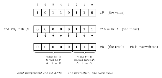
Figure 32: Why a mask works, one column at a time. Two rows of bits, an arrow down out of each column into a result row that overwrites the destination: here and r8, r16 with the mask 0x07, extracting the low three bits. The eight columns never interact — one mask bit decides one result bit, a 1 passing the value’s bit through and a 0 forcing it to zero — and all eight happen at once in a single instruction. Choosing a mask is therefore nothing more than deciding, position by position, which bits to keep.
Read Figure 32 column by column and the technique stops needing to be memorised: since the columns are independent, choosing a mask is just choosing, for each of the eight positions separately, whether that position gets passed through or forced.
The three identities that make it work
Each of AND, OR and XOR has a value that passes a bit through unchanged and a value that forces it. That pairing is the whole technique.
| \(X \cdot 0\) | \(X \cdot 1\) | \(X \cdot X\) | |
|---|---|---|---|
| AND | \(= 0\) | \(= X\) | \(= X\) |
| \(X + 0\) | \(X + 1\) | \(X + X\) | |
|---|---|---|---|
| OR | \(= X\) | \(= 1\) | \(= X\) |
| \(X \oplus 0\) | \(X \oplus 1\) | \(X \oplus X\) | |
|---|---|---|---|
| XOR | \(= X\) | \(= \overline{X}\) | \(= 0\) |
Reading off the pass-through and force columns gives the operation to reach for:
| To do this to the selected bits | Use | Mask bit = 1 on | Mask bit = 0 on |
|---|---|---|---|
| Clear them to 0 | AND |
the bits to keep — \(X \cdot 1 = X\) | the bits to clear — \(X \cdot 0 = 0\) |
| Set them to 1 | OR |
the bits to set — \(X + 1 = 1\) | everything else — \(X + 0 = X\) |
| Toggle them | EOR |
the bits to flip — \(X \oplus 1 = \overline{X}\) | everything else — \(X \oplus 0 = X\) |
| Extract them (others zeroed) | AND |
the bits to keep — \(X \cdot 1 = X\) | the bits to discard — \(X \cdot 0 = 0\) |
Note the asymmetry: AND’s mask is 1 on the bits you keep, whereas OR’s and XOR’s masks are 1 on the bits you act on. Getting that backwards is the usual bug — with AND you write the mask for what survives, with the other two for what changes.
\(X \oplus X = 0\) is the other one worth remembering: XORing a register with itself is the cheapest way to zero it.
In AVR assembly
The masks are ordinary constants, so the bitwise instructions of avr-instructions do the work. On AVR the immediate forms (andi, ori) only reach r16–r31; for a low register, load the mask into a high register and use the two-register form.
Extract the least significant three bits of r7 into r8, other bits of r8 zero.
    mov  r8, r7          ; copy the source
    ldi  r16, 0x07       ; mask 0000 0111 — keep the bottom three
    and  r8, r16         ; everything else forced to 0
Toggle the most significant four bits of r9, other bits unchanged.
    ldi  r16, 0xF0       ; 1111 0000 — flip the top four
    eor  r9, r16         ; bottom four XOR 0, so unchanged
Clear the least significant four bits of r10, other bits unchanged.
    ldi  r16, 0xF0       ; 1 on the bits to KEEP
    and  r10, r16        ; bottom four AND 0 -> 0
Set the most significant four bits of r11 to 1, other bits unchanged.
    ldi  r16, 0xF0       ; 1 on the bits to set
    or   r11, r16        ; bottom four OR 0, so unchanged
Note how 0xF0 appears as the mask in three of these with three different meanings — keep, flip, set — decided entirely by the instruction it is paired with.
In C
The same four operations with C’s bitwise operators (c-operators), which is how every AVR C program touches its ports. The masks are the same; the immediate-register restriction disappears, since the compiler chooses the registers.
| Operation | Operator | Example | Reads as |
|---|---|---|---|
| Clear particular bits | & with 0s on the bits to clear |
var = PINB & 0x0F; |
keep the low nibble, zero the high |
| Test particular bits | & with a 1 on the bit to test |
if (PINB & 0x02) … |
true if bit 1 is set |
| Set particular bits | \| with 1s on the bits to set |
PORTC = PINB \| 0x80; |
force bit 7 to 1 |
| Invert particular bits | ^ with 1s on the bits to flip |
PORTC = PINB ^ 0x0F; |
flip the low nibble |
Write the mask as a shift, not a hex constant: (1<<5) says bit 5 where 0x20 has to be decoded, and the header files name every register bit as a bit number for exactly this use (c-preprocessor-and-avr-headers):
DDRB  = (1<<5);                 /* bit 5 output, every other bit input: REPLACES the register */
DDRB |= (1<<4) | (1<<3);        /* bits 3 and 4 output, the rest unchanged: read-modify-write */
DDRB &= ~(1<<3);                /* bit 3 back to input, the rest unchanged                    */
PORTC ^= (1<<0);                /* toggle bit 0                                              */
TCCR1B = (1<<WGM12) | (1<<CS11) | (1<<CS10);   /* named bits, ORed into one value            */
The difference between the first two lines is the one that bites: = writes the whole register and silently sets the other seven bits to 0, |= ORs into what is already there. In assembly the second line is three instructions — in, ori, out — and the C compiler emits exactly those (week8-lab-avr-c-programming). For a single-bit clear the mask is the complement of the set mask, ~(1<<n), which is why clear bit 3 is &= ~(1<<3) and not &= (1<<3).
The test idiom needs no comparison. PINB & 0x02 is 0x02 when bit 1 is set and 0 when it is not, and C treats any non-zero value as true (c-control-flow) — so if (PINB & 0x02) is right and if ((PINB & 0x02) == 1) is always false, because the masked value is 2, never 1.
Set, clear and toggle on an I/O register
Changing one bit of an I/O register, and only that bit, is one of three lines. Each reads the register, combines it with a one-bit mask and writes it back:
| To | Write | The mask | Why the other bits survive |
|---|---|---|---|
| set bit n | REG \|= (1<<n); |
a 1 on bit n | \(X + 0 = X\) |
| clear bit n | REG &= ~(1<<n); |
a 0 on bit n, 1s elsewhere | \(X \cdot 1 = X\) |
| toggle bit n | REG ^= (1<<n); |
a 1 on bit n | \(X \oplus 0 = X\) |
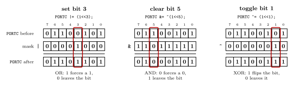
Figure 33: Set, clear and toggle on one register byte. Each panel starts from the same value of PORTC, 0110 0101, and changes one bit, outlined, with a single read-modify-write. The mask is a 1 shifted to the bit’s position, complemented for a clear. In every other column the mask holds the value that leaves a bit alone: 0 for OR and XOR, 1 for AND. Set gives 0110 1101, clear gives 0100 0101 and toggle gives 0110 0111, and each time the other seven bits are untouched.
Toggle is not enable. TIMSK2 ^= (1<<OCIE2A); turns the timer 2 compare A interrupt on only if it was off, and a second run turns it off again. To enable whatever the bit was before, set it with |=; to disable, clear it with &= ~. Toggling is for things meant to alternate, like an LED blinking.
The register has to be one that stores what is written. PORTx and DDRx do. PINx does not: it reads the pins, and on the ATmega324A a 1 written to one of its bits toggles the matching PORTx bit, so a read-modify-write on PINx changes the wrong bits (avr-io-ports).
Writing register bits by name
When setting or clearing bits of an I/O register, be explicit about which bits. Three ways to write the same value, from worst to best:
TCCR1B = 10;                          /* poor:   a number                    */
TCCR1B = 0x0A;                        /* better: the pattern, 0000 1010      */
TCCR1B = (1<<WGM12) | (1<<CS11);      /* best:   the bits, by name           */
WGM12 is bit 3 of TCCR1B and CS11 is bit 1, so all three are 0000 1010. Only the last says which bits, so a reader can check them against the datasheet without decoding anything: CTC mode, clock divided by 8 (avr-timers-and-counters). It costs nothing, either. The compiler works out (1<<WGM12) | (1<<CS11) while compiling, and all three lines become the same instructions.
The names are bit numbers. The device header that <avr/io.h> includes defines every bit name as the bit’s position in its register:
#define WGM02 3A name is not a mask; 1<< makes it one (c-preprocessor-and-avr-headers). The names are the datasheet’s, and the datasheet has errors in places, so the I/O register summary at the back is the one to check a name against.
Assembly uses the same names. In ldi r16, (1<<WGM02)|(1<<CS01) the assembler works out the constant, 0x0A, and the instruction stored is ldi r16, 0x0A.
A name belongs to one register. WGM12 and WGM02 are both 3, so (1<<WGM12) written into TCCR0B sets WGM02, and the compiler cannot notice, because all it sees is the number 3. Pair each name with the register whose datasheet entry defines it. The same byte 0x0A is CTC mode in TCCR1B and a reserved mode in TCCR0B (2026-10-05-more-io).
Masking sets the status flags too
Status register flags will be set also — a mask operation is a real ALU operation, not a free one. AND, OR and EOR all clear V and set N and Z from the result (C is untouched); see avr-architecture.
That side effect is often the actual point. andi r16, 0x01 keeps only bit 0, so:
\[Z = 1 \iff \text{bit 0 of } \texttt{r16} \text{ is } 0 \iff \texttt{r16} \text{ is even}\]
which makes a single masked AND an even/odd test. Any single-bit mask turns the Z flag into a test of that one bit — and tst rd, which is just and rd, rd, is the degenerate case that tests the whole register against zero.
Common mistakes
&= (1<<n)to clear bit n. That keeps bit n and clears the other seven. A clear’s mask is the complement,~(1<<n).=where|=was meant.DDRB = (1<<5)makes PB5 an output and every other pin of port B an input.- A bit name without the shift.
TCCR1B |= WGM12;ORs in the number 3,0000 0011, which setsCS11andCS10, clock divided by 64, and leavesWGM12alone. - A bit name in the wrong register.
(1<<WGM12)inTCCR0BsetsWGM02. ^=to enable. A toggle enables only from off; run twice, it disables.- A read-modify-write on
PINx. WritingPINxtoggles outputs, so it cannot clear or set a bit. - Getting AND’s mask backwards. With AND the 1s mark the bits to keep; with OR and XOR they mark the bits to change.
if ((x & mask) == 1). The masked value is the mask’s own value, so the test is false unless the mask is bit 0. Test for non-zero.
See also
- boolean-algebra · avr-instructions · avr-architecture
- avr-io-ports — one bit of a port in C and assembly, and why
PINxis different - avr-timers-and-counters — the
TCCRnBfields named in the examples - 2026-10-05-more-io — Lecture 19: poor, better and best,
TIMSK2toggled - week5-lab-avr-assembly-one — Lab 9, where these snippets are the exercise
- week8-lab-avr-c-programming — Lab 11, the same operations in C · c-operators · c-preprocessor-and-avr-headers
C Operators
The operators the course uses, in groups — arithmetic, comparison, bitwise, logical, assignment — with the two families that look alike and are not, the shift operators and what they compile to, and the prefix/postfix rule. First met in 2026-09-07-introduction-to-embedded-c-programming; the signed/unsigned shift rule is in 2026-09-10-more-c-programming-on-the-avr. Types are in c-language-basics.
Binary operators
| Group | Operator | Meaning | AVR instruction behind it |
|---|---|---|---|
| arithmetic | + |
addition | add, adc |
- |
subtraction | sub, sbc |
|
* |
multiplication | mul |
|
/ |
division (integer, truncates toward 0) | a library routine — the AVR has no divide | |
% |
remainder (integer) | likewise | |
| comparison | > >= < <= |
ordering | cp then a branch on the flags |
== |
equal | cp then breq |
|
!= |
not equal | cp then brne |
|
| bitwise | & |
bitwise AND | and, andi |
\| |
bitwise OR | or, ori |
|
^ |
bitwise XOR | eor |
|
| logical | && |
logical AND | compare-and-branch sequences |
\|\| |
logical OR | ||
| assignment | = |
assignment | a mov, ld/st, or in/out — whatever the two sides are |
The instructions in the last column are in avr-instructions.
A comparison produces a value: 1 if true, 0 if false. So a > b is an ordinary expression that can be assigned, and (a > b) + (c > d) counts how many are true.
Unary operators
| Operator | Meaning | Example | AVR |
|---|---|---|---|
! |
logical not | !A ≡ Ā |
test-and-branch |
~ |
one’s complement (invert every bit) | ~A |
com |
- |
two’s complement (negate) | neg |
|
++ |
increment (prefix or postfix) | inc, or subi rd, -1 |
|
-- |
decrement (prefix or postfix) | dec |
Bitwise is not logical
The two pairs &/&& and |/||, and the pair ~/!, are the easiest mistake in C to make and the hardest to see.
- Bitwise
&,|,^,~work column by column: bit \(i\) of the result depends only on bit \(i\) of each operand. This is the eight-parallel-columns picture of bit-masking and theAND/OR/EOR/COMof avr-instructions. - Logical
&&,||,!treat each whole operand as true or false (non-zero or zero) and yield 1 or 0.
unsigned char a = 0x0F, b = 0xF0;

a & b      /* 0x00 — no column has a 1 in both  */
a && b     /* 1    — both are non-zero, so true */

~a         /* 0xF0 — every bit flipped           */
!a         /* 0    — a is non-zero, so "not a" is false */
a & b is zero and a && b is one, from the same two operands. Inside an if, if (PINC & 0x01) tests one bit, which is what is usually meant; if (PINC && 0x01) is true whenever anything on port C is high. The compiler accepts both.
== is not =
Read a = b as a ⇐ b.
=does.a = bcopiesbintoa. The arrow reading is the honest one: data flows right to left, the same destination first rule asmov rd, rrin avr-instructions.==asks.a == bis 1 if they are equal, 0 if not, and changes nothing.
if (a = 0) is legal C. It stores 0 in a, tests the stored value, and never takes the branch — silently.
Assignment shorthands
a += b is shorthand for a = a + b, and similarly -=, *=, /=, %=, &=, |=, ^=, <<=, >>=. a += 1 is the same as a++.
The three that matter most on the AVR are the bitwise ones, because they are the read-modify-write of a port in one line:
PORTA |= 0x01;      /* set bit 0, leave the rest    */
PORTA &= ~0x01;     /* clear bit 0, leave the rest  */
PORTA ^= 0x01;      /* toggle bit 0                 */
each a mask operation from bit-masking — and the ~ in the second is the reason the mask can be written as the bit to clear rather than as its complement.
Shifts
| AVR | ||
|---|---|---|
a << b |
a shifted left by b bits; 0 enters at the bottom |
lsl, b times |
a >> b |
a shifted right by b bits — logical if a is unsigned, arithmetic if a is signed |
lsr or asr, b times |
A left shift by \(n\) multiplies by \(2^n\); a right shift by \(n\) divides by \(2^n\), rounding toward \(-\infty\) for signed values. Two examples: 1 << 5 is \(1 \times 2^5 = 32\) and 3 << 4 is \(3 \times 2^4 = 48\) — worked in bits in the shift figure of 2026-09-07-introduction-to-embedded-c-programming.
The type picks the instruction. In assembly the programmer chose lsr or asr and thereby declared whether the byte was unsigned or signed (2026-09-03-instruction-set-architecture-part-2). In C there is one >>, and the declaration made the choice already:
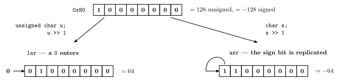
Figure 34: One operator, two instructions. The same bit pattern 10000000 is shifted right by one under two declarations. As unsigned char it means 128, the compiler emits lsr, a 0 enters at the top, and the result is 64. As char it means \(-128\), the compiler emits asr, the sign bit is copied back into the top, and the result is \(-64\). Both are the correct halving of what the bits were declared to mean.
1 << n is the mask with only bit \(n\) set. The AVR headers name every flag and pin as a bit number, so 1 << FLAG_NAME — with FLAG_NAME == 5 giving 00100000 — is how a mask is written from a name rather than a magic constant (c-preprocessor-and-avr-headers). Combined with the shorthands above:
PORTA |= (1 << 5);     /* set bit 5     */
PORTA &= ~(1 << 5);    /* clear bit 5   */
if (PINC & (1 << 3))   /* test bit 3    */
Prefix and postfix ++ and --
a++ and ++a both add one to a. They differ in what the expression is worth:
| Order | Rule | |
|---|---|---|
postfix a++ |
use value, change value | the expression is the old a; then a becomes a + 1 |
prefix ++a |
change value, use value | a becomes a + 1; the expression is the new a |
Every use is two statements in disguise, and only the order differs:
int a,b,c,d,e;
a = 4;
b = a++;    /* b=a;   a=a+1; */   /* b=4, a=5 */
c = --a;    /* a=a-1; c=a;   */   /* a=4, c=4 */
d = ++a;    /* a=a+1; d=a;   */   /* a=5, d=5 */
e = a--;    /* e=a;   a=a-1; */   /* e=5, a=4 */
Final values: a=4, b=4, c=4, d=5, e=5.
Worked: a = 1; b = 3; b += a++; leaves b = 4, because b += a++ is b = b + a with the old a, and only then a = a + 1. An answer of 5 applies the increment first, which is what ++a does.
On its own line, a++; and ++a; are indistinguishable: the value of the expression is thrown away, and only the change remains. The difference exists only when the expression is used — assigned, passed, indexed, as in values[9] = values[8]++; (c-pointers-and-arrays).
Precedence
The one place precedence bites is the SQUARE(1+2) example in c-preprocessor-and-avr-headers, where * binding tighter than + turns (1+2*1+2) into 5. The rule the course relies on is the schoolroom one — *, /, % before +, - — and the practical advice is parenthesise anything you would have to think about. Two cases to know because the natural reading is wrong:
&binds looser than==, sox & 1 == 0isx & (1 == 0), i.e.x & 0. Write(x & 1) == 0.<<binds looser than+, so1 << n + 1is1 << (n + 1). Write(1 << n) + 1if that is what is meant.
These are the two that catch AVR code in particular.
See also
- c-language-basics · c-control-flow · c-pointers-and-arrays · c-preprocessor-and-avr-headers
- bit-masking — the set/clear/toggle/extract patterns the bitwise operators write
- avr-instructions — the instructions each operator compiles to, including
lsl/lsr/asr - boolean-algebra — the laws behind
&,|,^and~ - floating-point-numbers — integer
/against floating point on the AVR:PINA / 3andPINA * 0.334f - 2026-09-07-introduction-to-embedded-c-programming — Lecture 13 · 2026-09-10-more-c-programming-on-the-avr — Lecture 14
Combinational Logic Blocks
Reference note for the standard combinational building blocks: the adder-subtractor, the multiplexer, and the decoder. See logic-gates for the gate symbols/truth tables and boolean-algebra for the notation used below.
What makes a circuit combinational
A combinational circuit is a combination of logic gates with \(n\) inputs and \(m\) outputs:
- Each output can be expressed as a function of the \(n\) input variables.
- The output depends on the current inputs only — there is no memory of previous inputs. (Contrast with sequential-circuits, where the output also depends on stored state.)
- It can always be written as a truth table with \(n\) input columns, \(m\) output columns, and \(2^n\) rows (one per possible input combination).
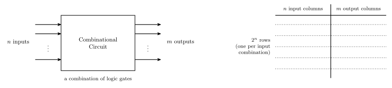
Figure 35: The general shape of a combinational circuit and the truth table it is always equivalent to. The row count \(2^n\) depends only on the number of inputs, and the output column count \(m\) only on the number of outputs — so a block with six inputs needs 64 rows however few gates are inside it.
Binary subtraction
\(A - B\) is usually implemented as \(A + (-B)\), where:
- \(A\) and \(B\) are multi-bit quantities;
- “+” here means addition, not OR;
- \(-B\) means the two’s complement of \(B\) (see binary-number-representations).
The two’s complement of \(B\) is calculated by flipping all the bits and adding 1:
\[-B = \bar B + 1\]
So a subtractor is just an adder with two extra pieces: something that conditionally inverts \(B\), and something that adds the extra 1.
The controlled inverter (XOR trick)
We need a gate that flips a bit only sometimes: given a mode bit \(M\),
\[Z = \bar B \text{ when } M = 1, \qquad Z = B \text{ when } M = 0\]
From the XOR truth table: XOR with one input held at 0 passes the other input through unchanged, and XOR with one input held at 1 inverts it. So the gate is a 2-input XOR:
\[Z = B \oplus M\]
| M | B | \(Z = B \oplus M\) | Effect |
|---|---|---|---|
| 0 | 0 | 0 | pass through |
| 0 | 1 | 1 | pass through |
| 1 | 0 | 1 | invert |
| 1 | 1 | 0 | invert |

Figure 36: The controlled inverter: one XOR gate per bit, with the mode line on the second input. The two identities on the right are the whole trick, and they hold for any signal X — XOR against a constant 0 is a wire, XOR against a constant 1 is an inverter.
This is called a controlled inverter.
Adder-subtractor circuit
A 4-bit adder-subtractor is built from a 4-bit binary adder (a ripple-carry adder — see 2026-08-04-binary-arithmetic) plus four XOR gates:
- Data input \(A\) (\(A_0 \ldots A_3\)) goes straight into the adder’s \(A\) inputs.
- Data input \(B\) (\(B_0 \ldots B_3\)) goes into the adder’s \(B\) inputs via one XOR gate per bit; the second input of every XOR gate is the shared mode select line \(M\).
- \(M = 0\) means add, \(M = 1\) means subtract.
- The adder produces the data output \(S_0 \ldots S_3\), plus a carry-out \(C_4\) and taking a carry-in \(C_0\).
The carry-in. With \(M = 1\) the XOR gates supply \(\bar B\), and two’s complement needs \(\bar B + 1\) — the extra \(+1\) is supplied by feeding it in as the carry-in. With \(M = 0\) we want plain addition, which needs a carry-in of 0. Both cases are satisfied by
\[C_0 = M\]
so the mode select line is wired to both the XOR gates and the adder’s carry-in.
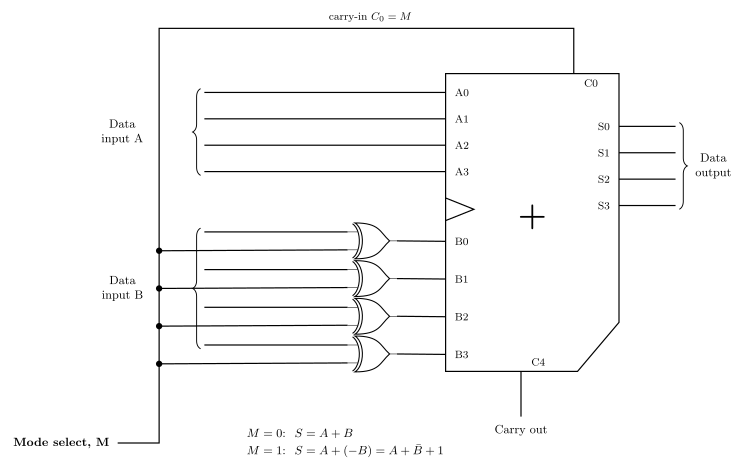
Figure 37: The 4-bit adder-subtractor. One mode line does two jobs: it conditions every bit of B through an XOR, and it is the adder’s carry-in. With M = 0 the XORs pass B through and the carry-in is 0, so the adder computes A + B; with M = 1 the XORs deliver B-bar and the carry-in is 1, so it computes A + B-bar + 1, which is A + (-B). No extra hardware is spent on the +1 at all.
The cost of subtraction is therefore four XOR gates and one wire on top of an adder — a 74HCT86 (quad 2-input XOR) plus a 74HCT283 (4-bit adder), see device-pinouts.
Multiplexer (mux)
A multiplexer — also called a data selector — has:
- \(2^n\) data inputs,
- 1 output,
- \(n\) control (or select) inputs, which select one of the data inputs to be “sent” or “steered” to the output.
Figure 38: The multiplexer logic symbol at two sizes, 4-to-1 and 2-to-1. Data inputs enter the tall left edge, the single output leaves the short right edge, and the select inputs enter from underneath. The number of select lines is what fixes the size: n selects steer 2^n data inputs.
4-to-1 multiplexer
Data inputs \(D_0 \ldots D_3\), select inputs \(S_1 S_0\), output \(F\). The logic symbol is the characteristic trapezoid with the data inputs on the wide (left) edge, \(F\) on the narrow (right) edge, and the select inputs entering the bottom.
Function table:
| \(S_1\) | \(S_0\) | \(F\) |
|---|---|---|
| 0 | 0 | \(D_0\) |
| 0 | 1 | \(D_1\) |
| 1 | 0 | \(D_2\) |
| 1 | 1 | \(D_3\) |
This is a function table, not a full truth table — the full truth table would need \(2^6 = 64\) rows for the six inputs \(S_1, S_0, D_0, D_1, D_2, D_3\). The function table’s four rows say the same thing far more compactly, which is why it is what gets drawn.
4-to-1 mux logic circuit implementation
- \(S_1\) and \(S_0\) each feed an inverter, giving \(\bar S_1\) and \(\bar S_0\) as well as the true forms.
- Four 3-input AND gates, one per data input. Each AND gate takes its data input plus the select-literal pair that identifies it: \(D_0\) with \(\bar S_1 \bar S_0\), \(D_1\) with \(\bar S_1 S_0\), \(D_2\) with \(S_1 \bar S_0\), \(D_3\) with \(S_1 S_0\).
- The four AND outputs feed a single 4-input OR gate whose output is \(F\).
Figure 39: A 4-to-1 multiplexer built from gates. The two inverters generate the complemented selects; the four vertical rails carry S1, S1-bar, S0 and S0-bar past every AND gate; each AND gate is one data input gated by the one select combination that names it, and the OR gate collects them. Only the dots are connections — every other crossing is two wires passing.
That is exactly the sum-of-products form:
\[F = D_0 \bar S_1 \bar S_0 + D_1 \bar S_1 S_0 + D_2 S_1 \bar S_0 + D_3 S_1 S_0\]
Only the AND gate whose select literals match the current \(S_1 S_0\) can be 1, so exactly one data input reaches the OR gate at a time. The other three AND gates output 0, and \(0\) is the identity for OR, so they contribute nothing.
The gate-level version needs 3-input ANDs and a 4-input OR, neither of which exists in the lab kit (see device-pinouts) — building this from the available 2-input chips means cascading them.
2-to-1 multiplexer
Data inputs \(D_0\) and \(D_1\), one control input \(S_0\), output \(F\).
Function table:
| \(S_0\) | \(F\) |
|---|---|
| 0 | \(D_0\) |
| 1 | \(D_1\) |
Expanded to a full truth table over all three inputs (\(2^3 = 8\) rows):
| \(S_0\) | \(D_0\) | \(D_1\) | \(F\) |
|---|---|---|---|
| 0 | 0 | 0 | 0 |
| 0 | 0 | 1 | 0 |
| 0 | 1 | 0 | 1 |
| 0 | 1 | 1 | 1 |
| 1 | 0 | 0 | 0 |
| 1 | 0 | 1 | 1 |
| 1 | 1 | 0 | 0 |
| 1 | 1 | 1 | 1 |
i.e. \(F = D_0 \bar S_0 + D_1 S_0\). When \(S_0 = 0\) the output tracks \(D_0\) and ignores \(D_1\); when \(S_0 = 1\) it tracks \(D_1\) and ignores \(D_0\).
A quad 2-input multiplexer is available as an off-the-shelf IC — the 74HCT157, see device-pinouts.
Using a mux to implement a logic function
Because the data inputs can be tied to constant 0 or 1, an \(n\)-select mux with its selects wired to the function’s variables can implement any function of those \(n\) variables: set data input \(D_i\) to the value the function should take when the selects equal \(i\). The function table is the truth table of the function, read off directly. See the worked question in 2026-08-06-combinational-logic.
Decoder
A decoder converts an \(n\)-bit input to a logic 1 on exactly one of its \(2^n\) outputs (the one whose index equals the input value); all other outputs are 0.
Figure 40: The decoder as a block: n inputs in, 2^n outputs out, and the shape widens accordingly. It is the mux’s opposite — a mux funnels 2^n inputs down to one output under n selects, a decoder fans n inputs out to 2^n outputs.
3-to-8 decoder
Inputs \(A, B, C\) (with \(A\) the most significant), outputs \(D_0 \ldots D_7\).
| A | B | C | \(D_0\) | \(D_1\) | \(D_2\) | \(D_3\) | \(D_4\) | \(D_5\) | \(D_6\) | \(D_7\) |
|---|---|---|---|---|---|---|---|---|---|---|
| 0 | 0 | 0 | 1 | 0 | 0 | 0 | 0 | 0 | 0 | 0 |
| 0 | 0 | 1 | 0 | 1 | 0 | 0 | 0 | 0 | 0 | 0 |
| 0 | 1 | 0 | 0 | 0 | 1 | 0 | 0 | 0 | 0 | 0 |
| 0 | 1 | 1 | 0 | 0 | 0 | 1 | 0 | 0 | 0 | 0 |
| 1 | 0 | 0 | 0 | 0 | 0 | 0 | 1 | 0 | 0 | 0 |
| 1 | 0 | 1 | 0 | 0 | 0 | 0 | 0 | 1 | 0 | 0 |
| 1 | 1 | 0 | 0 | 0 | 0 | 0 | 0 | 0 | 1 | 0 |
| 1 | 1 | 1 | 0 | 0 | 0 | 0 | 0 | 0 | 0 | 1 |
The 1 always sits in the column whose index is the binary value of \(ABC\).
Each row of the table is one minterm: the top row is \(\bar A \bar B \bar C\) and the bottom row is \(ABC\).
3-to-8 decoder logic circuit implementation
- Each of \(A\), \(B\), \(C\) is fanned out to an inverter, so all six literals \(A, \bar A, B, \bar B, C, \bar C\) are available on a vertical bus.
- Eight 3-input AND gates, one per output. Each taps the three literals matching its index:
\[D_0 = \bar A \bar B \bar C, \quad D_1 = \bar A \bar B C, \quad D_2 = \bar A B \bar C, \quad D_3 = \bar A B C\] \[D_4 = A \bar B \bar C, \quad D_5 = A \bar B C, \quad D_6 = A B \bar C, \quad D_7 = ABC\]
Figure 41: A 3-to-8 decoder built from gates. Three inverters generate the complements onto six vertical rails; each of the eight AND gates taps the one literal triple that matches its index, so it is the minterm for that input combination. Exactly one AND gate can be high at a time, which is the decoder’s defining property.
Each AND gate is the minterm for one input combination, so exactly one is high at any time.
Using a decoder to implement a logic function
Because a decoder hands you every minterm of its inputs on a separate wire, any function of those inputs is just an OR of the minterm outputs whose truth-table rows are 1. For example, take
\[F = \bar A \bar B \bar C + ABC\]
which is \(D_0 + D_7\) — one OR gate on two decoder outputs, with nothing else needed.
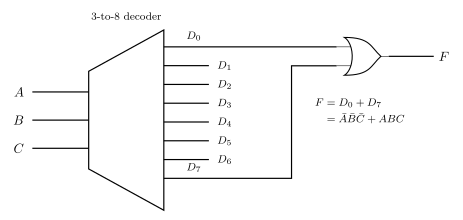
Figure 42: A function built on a decoder: F = A-bar B-bar C-bar + ABC is D0 + D7, so it costs a single OR gate on top of the decoder. Any function of A, B and C can be built this way — pick out the outputs for its true rows and OR them together.
This is the same idea as the mux trick above, approached from the other side: a mux picks one of \(2^n\) values, a decoder hands you all \(2^n\) minterms and you OR the ones you want.
See also
- 2026-08-06-combinational-logic — Lecture 4, where these blocks were introduced
- device-pinouts — the off-the-shelf parts: 74HCT157 (mux), 74HCT283 (adder), 74HCT86 (XOR)
- arithmetic-logic-unit — the ALU bit slice, which is a mux selecting between several function blocks
- binary-number-representations — two’s complement, on which the subtractor depends
CSSE2010 Diagram Notation
The drawing conventions this course actually uses, inferred from its own materials. This is the reference every later diagram in CSSE2010 should be checked against.
Scope. This note covers the diagram families that the two existing notation notes do not: gate symbols and logic diagrams, timing/waveform diagrams, state diagrams and state tables, block and datapath diagrams, register/memory layout diagrams, and the AVR architecture figures. It also records the algebraic and textual notation the figures depend on. For circuit-schematic rules (device IDs, gate letters, pin numbers, junction dots, power blocks, IO-board input/output pentagons) see circuit-schematics; for the 74-series pinouts and their schematic symbols see device-pinouts. Those two are not repeated here.
What was read
An honest statement of the sample, because most of what follows is inferred from drawings rather than stated in prose.
Guides — all three read in full (9 of 9 pages):
- CSSE2010/CSSE7201 Device Pinouts and Symbols (v4), pp. 1–2
- CSSE2010/CSSE7201 — Guide to Drawing Circuit Schematics (v2.3, Semester One 2016), pp. 1–2
- I/O Board User Manual, pp. 1–5
Lecture decks — 221 of 246 pages:
| Deck | Pages read | of |
|---|---|---|
| L01 Intro and Binary Numbers | 1–20 | 21 |
| L02 Intro to Logic Gates | 1–24 | 24 |
| L03 Binary Arithmetic | 8–17 | 17 |
| L04 Combinational Logic | 1–19 | 19 |
| L05 Flip-Flops | 4–19 | 19 |
| L06 Shift Registers | 3–17 | 17 |
| L07 Counters | 3–17 | 17 |
| L08 State Machines | 2–21 | 21 |
| L09 ALU and Control Unit | 3–22 | 22 |
| L10 AVR Introduction | 3–19 | 19 |
| L11 ISA Part 1 | 3–28 | 28 |
| L12 ISA Part 2 | 2–20 | 22 |
Unread: L01 p21, L03 pp1–7, L05 pp1–3, L12 pp21–22 — title, outline and admin pages in every case except L03 pp1–7 (number-representation recap, no new diagram family). Labs, past papers and the course profile were not sampled at all.
Citation format below: “L04 s10” means lecture deck 04, slide 10. Slide numbers printed on the slides match the PDF page numbers in every deck checked.
The course ships no notation guide for these diagram families
The three guides are hardware documents. Between them they settle schematic layout, device labelling, pin numbering and the physical IO board — nothing about gate-symbol family, waveform drawing, state diagrams, block diagrams or memory layout. The Device Pinouts and Symbols sheet comes closest: it has a “Logic Diagram Symbol” column (p. 1–2) that shows the gate shapes and the flip-flop/mux/adder block symbols, but it gives no rules, only examples.
So: everything in the sections below except the schematic rules is inferred from the drawings, and every entry is cited so you can check the inference.
Figure sources the slides cite
This matters more than it looks. L01 s8 says “No textbook required” — yet four different figure sources are credited across the semester, each bringing its own drawing style. There is no single house style.
| Source, quoted as printed | Where | What it supplies |
|---|---|---|
[Figure from Mano, "Digital Design", 3rd edition] |
L03 s16, L04 s4, L04 s10, L05 s17, L08 s3 | Ripple-carry adder, 4-to-1 mux circuit, sequential-circuit block diagram |
[Mano, Digital Design, 3rd ed.] (short form) |
L06 s6, L06 s8, L06 s9 | 4-bit register, 4-bit shift register |
Images taken from Instructor Resources of Digital Fundamentals, Thomas L. Flyod, Pearson Educations Inc., 2015 (misspelling in the original) |
L07 s4, s5, s7 | Shift-register type diagrams, digital-system application block diagram |
[Figure from Tanenbaum, "Structured Computer Organization"] — no edition given |
L09 s8 | Full ALU internal logic diagram |
[From ATmega324A datasheet] |
L11 s14 | AVR data and program memory maps |
Some datasheet extracts follow (prose, not a caption) |
L10 s9, covering s10–s11 | AVR CPU architecture, ATmega324A chip block diagram |
Source: Google Images |
L01 s4 | Photo collages only, not line art |
Tanenbaum is also cited in prose twice as the source of terminology, not figures: (Tanenbaum calls this Program Status Word) (L11 s19) and These addressing mode names are as per Tanenbaum "Structured Computer Organization" (L12 s16).
Consequence for a new diagram: the block-diagram idiom the course leans on most is Mano’s (five citations across four decks). If you redraw a block diagram and want it to look native, match Mano, not Floyd. Floyd appears in exactly one deck. See Inconsistencies — this is not a settled question.
Gate symbols and logic diagrams
Symbol family
Distinctive-shape symbols throughout — no IEC rectangles anywhere. AND is a flat-backed body with a semicircular nose; OR has a concave back and a pointed nose; NOT is a triangle with a bubble on its tip; NAND/NOR/XNOR are the base shape with a bubble on the output; XOR/XNOR add a second concave arc set back from the input edge.
Evidence: the definitional table at L02 s6–s8 (all seven gates), then every working diagram in the course — L02 s14, s18, s19, s22, s23; L03 s15; L04 s10, s14; L05 s10, s11, s13; L07 s3, s12; L09 s6, s7, s8, s10; L11 s6. Also the “Logic Diagram Symbol” column of Device Pinouts and Symbols p. 1–2.
Consistency: holds without exception across all 221 deck pages and all three guides. The course never names the family; the identification as ANSI/IEEE Std 91 distinctive-shape is mine, from the shapes.
Inversion bubble
A small open circle at the symbol boundary, always. On outputs it makes NAND/NOR/XNOR/NOT (L02 s6–s8). It is also legitimate on inputs, to express a De Morgan equivalent: L02 s22 draws OR-with-inverted-inputs ≡ NAND, and AND-with-inverted-inputs ≡ NOR, with bubbles sitting on the input leads at the body edge. Active-low control pins carry it too (74HCT157 ENABLE, Device Pinouts p. 2). Consistency: every occurrence, throughout.
Flow direction and wiring
- Inputs on the left, outputs on the right. Stated in words, twice: L02 s14 (“Inputs are conventionally on left” / “Outputs are conventionally on right”) and the Guide to Drawing Circuit Schematics p. 1. Held in every logic diagram sampled.
- Orthogonal routing only — wires run horizontally and vertically, turning at right angles; no diagonal segments in any figure. (L02 s14, s18; L04 s14; L05 s13; L11 s6.)
- Junction dot = connection. Crossing with no dot = no connection. L02 s14 labels both cases explicitly on the same figure (“Indicates Electrical Connection”, “No Connection”). Restated as error 2 of the schematics guide p. 2. Consistency: the single most-repeated drawing rule in the course.
- One line weight for all signals in a gate-level diagram. Thick lines appear only in datapath block diagrams (see below).
Labelling inside a logic diagram
- Gate-type names are written above the symbol only in the definitional table (L02 s6–s8: “AND”, “OR”, “NAND”, “NOR”, “XOR”, “XNOR”; the NOT symbol on s6 is left unnamed). In every working diagram the shape alone carries the function — no type label. (L02 s14, s18, s19; L03 s15; L04 s14; L09 s6.)
- Signal names: single uppercase letters for primary inputs (
A,B,C,D,E), andX,M,ForZfor outputs (L02 s6–s8, s14, s18; L03 s15; L04 s14). Complements carry an overline (Ā). - Intermediate signals are labelled on the wire, immediately at the gate’s output, with the expression they carry:
AB,AC,AB + AC,B + C,A(B + C)(L02 s19; L05 s16; L06 s5), or written above the wire (ĀBC,AB̄C,ABC̄,ABC— L02 s18). - Numbered gates: where a figure needs to refer to individual gates it puts a bare arabic numeral inside the gate body (L02 s18: inverters 1–3, ANDs 4–7, OR 8). Seen once. Extrapolate with caution.
- Signal rails: when one variable feeds many gates, it is run as a vertical rail crossing the whole figure, tapped with junction dots, and labelled at the top of the rail (L02 s18 — rails
A B C Ā B̄ C̄; L04 s14, the 3-to-8 decoder, same idiom). Two instances, two decks. - Sub-figure labels are lowercase letters in parentheses, centred under each variant:
(a) (b) (c) (d)(L02 s22; L05 s14, s15).
Block and MSI symbols
Multiplexer — trapezoid, wide edge left
Long parallel edge on the left carrying the data inputs stacked top-to-bottom (D0 … D3, or bare 0/1/2/3 when the inputs are anonymous); short parallel edge on the right with the single output; select inputs enter through the bottom sloping edge, labelled outside the body (S1 S0, SEL, DIRN, F1 F0).
Evidence: L04 s9, s10, s11, s12; L06 s12; L09 s6, s7, s10; L11 s6; Device Pinouts p. 2 (74HCT157, with SEL and ENABLE on the bottom edge). Consistency: five decks plus the guide — solid.
Decoder — trapezoid, wide edge right
The mirror flare: short edge on the left with the n inputs (A B C), long edge on the right with the 2ⁿ outputs (D0 … D7). (L04 s13.) Consistency: one figure only. The orientation is unmistakable in it, but it is a single instance.
Adder — trapezoid with a + in the body
Long edge left with the two operand groups and the carry-in at the top corner; short edge right with the sum group and the carry-out. A large + sits in the middle of the body. (L04 s7; Device Pinouts p. 2, 74HCT283.) The Floyd figure instead labels its adder block A Σ / B C_out (L07 s7) — see Inconsistencies.
D flip-flop — plain rectangle
D inside at the top-left, Q inside at the top-right, clock entering the lower-left edge, Q̄ under Q when the complement is needed. The triangular wedge (>) at the clock input means edge-triggered; no wedge means a level-triggered latch; a bubble in front of the wedge means falling-edge, no bubble means rising-edge. L05 s14 states all four cases explicitly as figures (a)–(d) with the caption “Triangle indicates edge-triggered (therefore flip-flop)”.
Evidence: L05 s5, s6, s14; L06 s4, s10, s11, s12; L07 s3, s8, s10, s11, s12; Device Pinouts p. 1–2. Consistency: the rectangle-with-wedge is universal; only the clock label varies (see Inconsistencies).
Asynchronous set/clear, when shown, are written SET above and CLR below inside the box (L07 s3, s12) and may be omitted entirely when unused — Device Pinouts p. 1 says so in words: “(Set and clear inputs can be omitted if not needed)”. Active-low asynchronous inputs are marked by overlining the name (P̄R̄Ē, C̄L̄R̄ — L05 s13) or by a bubble on the pin (Device Pinouts p. 1, 74HCT74). L06 s4 states the rule in prose: “The SET and CLR inputs are typically active-low”.
Register — rectangle with a name plate
Rectangle with the word Register written above the box, input pin names down the left edge, output pin names down the right, a plain vertical line joining the first and last name of a contiguous range (meaning “and all the ones between”), enable name centred at the bottom inside, clock wedge on the left edge. (L06 s15, the 4-stage 8-bit queue.) One figure.
ALU
Two shapes, both used, both in the same deck — see Inconsistencies. The notched trapezoid (wide edge up, a V-notch cut into the top edge, operands entering the top, result leaving the bottom, ALU lettered in the body) is the more common: L09 s15, s16, s20; L10 s10. The plain rectangle with ALU centred and heavy arrows on all four sides is used at L09 s5 and s9.
Timing and waveform diagrams
See timing-diagrams for what a timing diagram means; this is how it is drawn.
- Time runs left to right. Where the axis is marked at all it is a short solid horizontal arrow labelled
Timeplaced under or to the right of the waveform block (L04 s15, s18). Most figures omit it (L04 s16, s17; L05 s6, s8). - One horizontal track per signal, stacked vertically. The signal name sits to the left of its track, followed by a colon:
Input:,Output:,D:,CLK:,Q:,A:,B:. (L04 s15, s16, s17; L05 s6, s8.) Consistency: every timing figure sampled. - Two horizontal dashed reference lines bound each track — upper = logic 1, lower = logic 0. Where they are labelled, the labels read
Logic 1andLogic 0and sit at the end of the rails (L04 s15, s18). In most figures the rails are drawn but left unlabelled (L04 s16, s17; L05 s6, s8). - The waveform is a heavy solid black line, noticeably heavier than the dashed rails, riding on the lower rail for 0 and the upper for 1.
- Idealised transitions are vertical (zero rise/fall time): L04 s15, s16, s17; L05 s6, s8. Sloped edges appear only in the one figure whose subject is real timing — L04 s18, “Gates Aren’t Perfect … The Reality of Timing”, where the slope is the point.
- Input waveforms enumerate every input combination exactly once, in equal-width intervals. L04 s16 states it: “All combinations of inputs are covered”. For two inputs the pattern is A =
0 0 1 1, B =0 1 0 1across four equal intervals (L04 s16, s17). - Measured intervals are marked by dropping vertical dashed lines from the two instants and drawing a red double-headed arrow between them, labelled in blue (
Propagation delay,Fall time,Rise time). L04 s18 — one figure only, so treat the colour choice as that figure’s, not a rule. - Clock waveforms come two ways, both consistent within their purpose: a train of narrow rectangular pulses (mark shorter than space, no dashed rails) when the clock is the whole subject (L05 s18; L06 s7), and a full-height square wave on its own labelled track with rails when it sits alongside data signals (L05 s6, s8).
- A vertical dashed grid aligned to the clock edges may be laid over a multi-signal figure so the waveforms can be read against each other (L05 s8). One figure.
State diagrams
L08 s9 is the one slide in the whole course that states a diagram convention rather than merely demonstrating one. Everything here comes from it, plus the worked example on s18.
- A state is a circle divided by a horizontal chord. The state name goes in the upper half (bold); the output value(s) go in the lower half. Nothing else goes in the circle. (L08 s9, which prints the empty template
State Name/Output Value(s)next to two filled examples,S0/101andAlex/01.) - State names are free-form. The same slide sanctions both a systematic
S0,S1,S2,S3scheme (used in the worked example, L08 s18) and an arbitrary word (Alex). Outputs are written as a bare bit string with no separators or subscripts:101,01,00,11. - A transition is a plain single-headed arrow, labelled with a Boolean logic expression written above the arrow. “If expression is true, state transition is made.” (L08 s9.)
- An unlabelled arrow means “true” — always transition. Stated in words on L08 s9.
- Special case, exactly one input: the label degenerates to a bare
0or1. L08 s9 boxes this case in red and annotates it “Special case for only one input”. - Transition-label algebra is the ordinary Boolean notation of L02 s12: overbar for NOT,
.or juxtaposition for AND,+for OR. L08 s9’s own examples areZ,R̄Ē S̄ĒT̄, andA+B.C̄. - Completeness: “Each possible combination of inputs should be addressed exactly once for each state — i.e. transition arrows from each state must encompass all possibilities (exactly once).” (L08 s14.) This is a correctness rule, not a drawing rule, but it constrains what you draw.
- Layout: the one worked diagram (L08 s18) puts the states in a left-to-right row with forward transitions between neighbours and the wrap-around transition drawn as a long arc below the row. Single instance — the row layout is an example, not established as required.
State tables
Two forms, both defined on their own slide, both with an empty template printed so the column structure is unambiguous.
One-dimensional (L08 s15) — one row per (current state, input) combination, annotated “Every combination of state and inputs”:
| Current State | Input U | Next State | Outputs | |
|---|---|---|---|---|
| Q1 | Q0 |
Two-dimensional (L08 s16) — one row per state (“One row per state”), with the next-state column split by input combination (“Every combination of inputs”):
| Current State | Next State | Outputs | ||
|---|---|---|---|---|
| Ū | U | Q1 | Q0 |
Structural conventions common to both: headers bold and centred; a heavy rule under the header block and heavy vertical rules between column groups, thin rules inside a group; the individual output bits are sub-columns under a single spanning Outputs header; the input name appears in the header, not just its values.
For a counter with no external input, the same table is written with the next-state columns named after the flip-flop D inputs rather than the state: Current State (Q₁, Q₀) | Next State (D₁, D₀) (L07 s11). L08 s21 lists the design pipeline these tables sit in: state definition → state diagram → state table (1D or 2D) → state encoding → Boolean expressions → logic diagram → Logisim → hardware.
The characteristic table of a flip-flop uses different headers again: D | Q(t+1), with the right-hand column glossed “What the output will be on the next clock edge” (L05 s7).
Block and datapath diagrams
- Plain rectangles. No rounded corners, no drop shadows, no fill in the line-art figures. The block name is centred inside, on one or two lines. (L04 s8; L05 s17; L06 s6; L07 s16; L08 s3, s7; L09 s15, s16.)
- Flow left to right; feedback routed around the outside, usually below the blocks, returning to the left edge of the first block (L05 s17; L06 s6; L07 s16; L08 s3, s7). Consistency: every sequential-circuit block diagram in the course, across four decks.
- Every connection gets an arrowhead at its destination.
- The clock enters on its own labelled stub, not bundled with the data inputs —
Clock pulsesentering from below-left in the Mano figures (L05 s17; L06 s6; L08 s3),Clockentering from above in the UQ redraw (L08 s7). - Multi-bit paths are drawn heavy, single-bit control thin. L09 s15/s16 draw the A, B and Dest buses as thick black arrows against thin control lines; the caption “Buses (A,B,C)” points at them. L09 s5 and s9 draw the ALU’s
A,B,OutputandFunction/Controlas heavy arrows with the width lettered beside them (n,n,n,m). - Grouped signals are collected with a curly brace and one text label rather than labelled individually:
Data input A,Data output(L04 s7);Control registers,To and from memory(L09 s15);Before/Today(L12 s2); the IO-board input/output groups (Device Pinouts p. 2). - Anonymous repetition uses a vertical ellipsis between the first and last drawn line, with the count given in words beside the group: “n inputs”, “m outputs” (L04 s8).
- Bus width is marked two ways — see Inconsistencies.
Register and memory layout diagrams
Bit fields
A single row of equal-width boxes, MSB on the left, LSB on the right. Bit positions are numbered above the boxes, descending left to right and ending at 0. Values or field names go inside the boxes.
Evidence: L01 s12 (a byte, 0 1 0 1 0 1 1 1), s13 (positions 9 8 7 … 0 above, powers 2⁹ … 2⁰ and decimal weights 512 … 1 inside), s16 (MSB/LSB called out by red arrows to the extreme boxes), s17; L10 s15. Consistency: every bit-field figure. L01 s16 states the underlying rule: “the MSB is worth 2^(n-1)”.
The AVR-datasheet register diagram
For a named hardware register the three-row datasheet form is used: bit numbers 7 … 0 above the row of boxes, flag names inside the boxes (bold), an R/W access row underneath, and an initial-value row (0) under that. (L10 s15, the AVR status register I T H S V N Z C.) One figure in the sampled decks, but it is verbatim datasheet form and is the obvious template for any other AVR register.
Memory maps
L11 s14, the one memory map with an explicit source ([From ATmega324A datasheet]):
- Vertical stack of rectangles, lowest address at the top, highest at the bottom.
- Hex addresses written outside, to the right, aligned with the region boundaries — as a range for a fully-specified region (
0x0000 - 0x001F) or as the single start address of an open region (0x0100), with the final address at the bottom (0x08FF). - Hex is written
0x+ a fixed number of digits, four for the address space (0x0000), two for the register file (0x00…0x1F, L11 s22). - Region names inside the boxes, with the size in parentheses where useful (
Internal SRAM (1024/2048/4096/16384 x 8)). - Grey fill for the large or coarsely-described regions, white for the enumerated ones.
- A diagonal break across the block shows the drawing is not to scale (between Application Flash Section and Boot Flash Section).
- Column heading above each stack (
Data,Program Memory).
The generic memory-organisation figure (L11 s5) agrees on direction — addresses 0 1 2 3 … down the left side, increasing downward — and adds a double-headed arrow across the top labelled Cell width. The alignment figure disagrees; see Inconsistencies.
The register file
L11 s22: vertical stack, R0 at the top through R31 at the bottom, hex address to the right of each row, an ellipsis row ... for the elided middle, a heavy horizontal rule at the R15/R16 boundary marking the split that matters for ldi, and free text further right for the X/Y/Z aliases (X-register Low Byte, etc.).
Shift and rotate
L12 s10, s11: the printed figure is only a row of empty boxes. The direction arrows inside the boxes, the 0 entering the vacated end, the separate small box labelled C for the carry, and the wrap-around arc for a rotate are all drawn in the lecturer’s ink. Record this as the idiom the course uses, but note that nothing about it is printed — see Not established by the source.
AVR architecture figures
- The AVR CPU architecture diagram (L10 s10) and the ATmega324A chip block diagram (L10 s11) are datasheet reproductions, introduced only by the prose line “Some datasheet extracts follow” on L10 s9. Neither carries a caption. The only in-figure datasheet attribution anywhere is on the memory maps, L11 s14.
- CPU diagram style: black line art, no fill. The 8-bit data bus is a heavy vertical black bar running the full height, labelled
Data Bus 8-bitat the top. Blocks attach to the bus with double-headed arrows; instruction and control flow use thin single-headed arrows. The ALU inside is the notched trapezoid. Path labels that run vertically are set as rotated text (Direct Addressing,Indirect Addressing). Block names are two or three centred lines (Flash Program Memory,32 x 8 General Purpose Registers,Instruction Decoder,Data SRAM). - Chip-level diagram style (L10 s11): a dashed rectangle is the package boundary, with pin and port names outside it (
VCC,GND,RESET,XTAL1,XTAL2,PA7..0,PB7..0,TOSC2/PC7). A heavy solid outline inside is the internal bus, drawn with an arrowhead to show its direction. Peripherals are plain rectangles named for the function, with the width in parentheses for ports (PORT A (8)). Pin ranges are writtenPA7..0, high first. - The generic CPU figure the AVR specialises (L09 s3, s4; L10 s3) is a heavy outer rectangle labelled
CPUcontaining three filled boxes —Control Unit,Arithmetic Logic Unit (ALU),Registers— withPrimary Memoryas a separate box outside it. This one is filled with colour (green, cyan, lilac), used only to separate adjacent blocks. See avr-architecture and cpu-organisation.
Truth tables and function tables
- Inputs first (left), outputs last (right), separated by a heavier vertical rule. (L02 s6–s10; L03 s11, s14; L04 s11, s13; L05 s10.) Consistency: every truth table sampled.
- Rows in ascending binary counting order of the input columns, starting from all-zeros, all 2ⁿ of them. (Every table sampled.) L02 s13 states the underlying instruction: “Lists output for all 2ⁿ combinations of inputs — Best to list inputs in a systematic way”.
- Column headers are the bare signal names, bold. No units, no types.
- Function tables for MSI blocks list only the selector combinations, and the output column holds the name of the selected signal, not a bit:
S1 S0 | Fwith entriesD0,D1,D2,D3(L04 s9, s11). The header is called out asFunction table(L04 s9) orFunction Table(L04 s11). - A highlighted cell or row uses a pale fill — pale orange for the active decoder output (L04 s13), pale grey for the changing bits of a counting sequence (L07 s9).
- Visual styling of tables is not fixed — see Inconsistencies. Only the column semantics and row ordering are stable.
- Multi-column comparison tables (Intel-64 vs AVR data-type support, L12 s18) use a check mark
✔for “supported” and an empty cell for “not supported” — no cross, no “N/A”.
Boolean and textual notation
L02 s12 is titled “Boolean Algebra conventions” and states them outright — the only place in the course where notation is legislated rather than demonstrated:
- Inversion: overline.
NOT(A) = Ā, “pronounced as A bar”. - AND: a dot, or implied by adjacency.
AND(A,B) = AB = A.B. - OR: a plus sign.
OR(A,B,C) = A+B+C. - XOR:
⊕.XOR(A,B) = A⊕B = ĀB + AB̄. - The overline extends over exactly the sub-expression negated:
NAND(A,B,C) = A̅B̅C̅as one bar overABC;NOR(A,B) = A̅+̅B̅as one bar overA + B. Nested negation stacks bars (L02 s22:A̿ + B̿).
Held throughout the semester (L02 s16–s23; L03 s14; L04 s10; L07 s11, s14; L08 s9; L09 s11).
Beware the operator clash the course flags itself: in an arithmetic context + means addition, not OR — L04 s5 says “‘+’ in this case means addition (not OR)”.
Indexed signals take subscripts: Q₁, Q₀, D₁, D₀, S₁, S₀, A₃…A₀, C₄, F₁, F₀ (L03 s16; L04 s9; L07 s10–s12; L09 s6, s10). Not universally — see Inconsistencies.
Numbers
- Radix by subscript:
26₁₀,101₂,101₁₆,8₁₀ - 9₁₀(L01 s19, s20; L09 s22). - Radix by prefix:
0x(C and AVR),$(AVR assembly),0b(binary), leading0(octal). L01 s20 lists every alternative in a table and marks these ones “We’ll mostly use these”, ruling out the trailing-h, trailing-q, trailing-b,@and%forms. - Binary literals are grouped in fours with a space:
0000 1101 0111 0111,00001010,1110 KKKK dddd KKKK(L01 s18; L03 s8, s9; L10 s4, s16–s18). Short literals under about 8 bits are often left ungrouped (00001111, L11 s16).
AVR assembly and machine code
- Machine-code layouts write fixed bits as
0/1and each variable field as a repeated letter, one letter per bit —0000 11rd dddd rrrr(ADD),1001 010d dddd 0000(COM),1110 KKKK dddd KKKK(LDI).d= destination register,r= source register,K= constant. Note the case split: register-field letters lowercase, the constant uppercase. (L10 s16, s17, s18.) - Register-transfer notation uses a left arrow:
r3 ← r3 + r4,r22 ← r22 + 1(L10 s8, s12, s13). - Multi-byte quantities are written as a
high:lowregister pair:r5:r4,r11:r10,r13:r14,R31:R30(L11 s22; L12 s12, s20). High byte first, always. - Code is set in a monospace font, and concrete examples in the body text are coloured red (
mov r3, r14,add r5,r6,ldi r16,73— L10 s12–s14). - Mnemonic case is not settled — see Inconsistencies.
Colour and annotation
Colour carries no defined meaning anywhere in this course. No slide and none of the three guides ever says what a colour signifies. What can be observed:
- Red is the usual colour for a callout pointing into a figure — an arrow plus a short label, sitting outside the drawing (L01 s13
Bit position,Value (Powers of 2); L01 s16MSB/LSB; L02 s14 the four connection callouts; L04 s4Full-adders; L09 s5Function/Control; L09 s15Buses (A,B,C); L11 s5Address/Cell width). - Blue is the usual colour for an explanatory label attached to a figure element (L04 s15
Logic 1/Logic 0, s18Propagation delay; L05 s15, s17Logic Gates; L09 s10Carry ripples through from right to left). - But the two are swapped freely. L04 s15 uses red for
Change in input causes output to change; L08 s15/s16 use red for both the brace and its explanation; L09 s20 uses red for theStatuscallout with a green-filled fact box beside it; L09 s15 uses purple. - Fills are decorative, used only to separate adjacent blocks: yellow for the levels-of-abstraction stack (L01 s9; L02 s5), green/cyan/lilac for the three CPU parts (L09 s3, s4; L10 s3), pale blue/green/lilac for the fetch-decode-execute fact boxes (L09 s13).
- Table highlighting is a pale fill on the cell or row of interest (L04 s13; L07 s9).
Handwritten ink on the slides is the lecturer’s live annotation, not part of the published figure. It is present on most technical slides, in red, blue, purple, green and orange, and the colour there tracks nothing but which pen was in hand — L11 s13 uses three ink colours in one worked example purely to separate three sub-workings. Nothing that exists only in ink should be treated as an established figure convention; where a convention below is ink-only it is flagged as such and repeated under Not established.
Inconsistencies
Places where the course does the same thing more than one way. None of these is resolved here — a decision is needed before a new diagram commits to one.
The ALU has two symbol shapes, in one deck. A plain rectangle with
ALUcentred and heavy arrows on four sides (L09 s5, s9), and a notched trapezoid with operands in the top and result out the bottom (L09 s15, s16, s20; also the AVR datasheet figure, L10 s10). Both are the ALU of the same machine, ten slides apart. Decision needed.The flip-flop clock input has four labels.
CLK(L05 s5, s6; L06 s4; L07 s10, s11, s12; Device Pinouts p. 2 on the 74HCT175),CK(L05 s14 — the very slide titled “D Latches and Flip-flops — Symbols Used”), italic serifC(L06 s8, s9 — the Mano figures), and lowercase italicclkas the net name on the wire (L06 s10, s11; L07 s15). Decision needed.The asynchronous inputs have three naming schemes.
SET/CLR(Device Pinouts p. 1, 74HCT74 schematic symbol; L07 s3, s12),P̄R̄Ē(preset) /C̄L̄R̄(L05 s13), andRwith a bubble (Mano’s register, L06 s8). Device Pinouts p. 2 gives the 74HCT175 only aC̄L̄R̄. Decision needed.“Current state” vs “present state”, and “next state” vs “Q(t+1)”. Printed slides say
Current State(L07 s11; L08 s15, s16); the lecturer’s worked tables sayPresent State(L07 s8, s14 — ink). The flip-flop characteristic table calls the next-state columnQ(t+1)(L05 s7) where the state table calls itNext State(L07 s11; L08 s15). Decision needed.Three textbook figure styles coexist, none declared canonical. Mano, Digital Design 3rd ed. — black-and-white line art, thin rules, italic serif signal names with subscripts (
B₃,A₃,C₄,S₀,SI,SO,CLK), plain square blocks with italicFAinside (L03 s16; L04 s4, s10; L05 s17; L06 s6, s8, s9; L08 s3). Floyd, Digital Fundamentals — pale-blue and beige filled blocks, magenta arrows and magenta text labels, serif(a) Serial in/shift right/serial outsub-captions (L07 s4, s5, s7). Tanenbaum, Structured Computer Organization — dense line art with dashed boxes grouping sub-circuits (L09 s8). And L01 s8 says there is no textbook. Decision needed: which family a redrawn figure should imitate.The same block diagram exists in two drawing styles. The sequential-circuit block diagram appears as the Mano original — thin rules, serif lowercase labels
Combinational circuit/Flip-flops/Clock pulses(L05 s17; L06 s6; L07 s16; L08 s3) — and as a UQ redraw in bold sans-serif with heavy borders (L08 s7, the Moore/Mealy slide). Same content, same course, different look. Decision needed.Memory addresses increase downward in some figures and upward in others. Downward: the generic cell diagram (L11 s5, addresses
0 1 2 3 …down the left), the AVR address-space maps (L11 s14,0x0000at the top), the register file (L11 s22,R0at the top), the endianness examples (L11 s16, s17). Upward: the alignment figure (L11 s10), where the row addresses0 8 16 24run bottom to top and the byte numbers within a row run high-to-low left to right (15 14 13 12 11 10 9 8). Decision needed.Hex is prefixed
0xin some places and$in others — sometimes on the same slide.0x: L10 s15 area, L11 s14 (0x0000), L11 s22 (0x1F), L11 s27 (“0 to 0x3F”), L12 s15 (andi r17, 0xBA).$: L11 s26 (“$20 to $FF”), L12 s15 (lds r15, $1234). L01 s20 blesses both. Decision needed.Assembly mnemonic case in the generic form. Uppercase:
MOV rd, rr,ADD rd, rr,AND rd, rr,LDI rd, K(L10 s12, s13, s14; L11 s25; L12 s4, s9). Lowercase bold-italic:in rd, P,out P, rr(L11 s27; L12 s5), and lowercase throughout the addressing-modes slide (andi,and,lds,ld— L12 s15, s16). Concrete examples are lowercase in print (mov r3, r14) but uppercase in the lecturer’s ink (ADD r10, r4, L12 s20). Decision needed.Register names:
R0–R31orr0–r31. Uppercase in the register-file figure (L11 s22) and the AVR architecture block (L10 s10,32 x 8 General Purpose Registers); lowercase everywhere in prose and code (L10 s12–s14; L11 s27; L12 s4–s6). Decision needed.Truth-table visual styling has three treatments. Dark-red header row with pink zebra striping (L02 s9, s10; L03 s11; L04 s11); plain black-on-white with a bold header and a heavy input/output divider (L02 s6, s7; L03 s14; L04 s13; L05 s10); light-grey header with grey cell highlighting (L07 s9). Column semantics and row order are stable across all three; only the appearance differs. Decision needed for a house table style.
Bus width is marked two ways. A short slash across the line with the width beside it (Device Pinouts p. 2, the
4-marked buses of the 74HCT157 and 74HCT283 logic-diagram symbols). Or the width simply lettered next to a plain arrow, no slash (L09 s5, s9 —n,n,m,n). Decision needed.The adder’s function glyph. A large
+in the trapezoid body (L04 s7; Device Pinouts p. 2). OrΣon the block’s output pin withA,B,C_outon the others (L07 s7, the Floyd figure). Decision needed.Indexed signals are subscripted inconsistently. Subscripted
Q₁,Q₀,D₁,D₀in the counter state table and its circuit (L07 s10, s11, s12). UnsubscriptedQ1,Q0in the state-table templates (L08 s15, s16) andS0,D0in the mux function table (L04 s9). Decision needed.
Not established by the source
Things a CSSE2010 diagram may well need that the materials simply do not settle. These are where invention risk lives.
- Karnaugh maps: entirely absent. No K-map appears on any of the 221 deck pages sampled, nor in any of the three guides. The course’s simplification path runs truth table → sum of products → Boolean identities → algebraic manipulation (L02 s16–s21), and De Morgan is done algebraically (L02 s21, s22). If a K-map is needed, everything about it is invention: cell ordering and whether the axes are Gray-coded, which variable goes on which axis, how variable labels are written along the edges, the style of the grouping loops, and the don’t-care mark.
- The initial/reset state of a state diagram. L08 s9 defines only the state circle and the transition arrow. The one worked diagram (s18) has no incoming arrow from nowhere, no double circle, no
resetlabel. How to mark the start state is unspecified. - Mealy outputs on a state diagram. L08 s6, s7 define both machine types, then s7 says “We’ll stick to Moore machines in this course”. The notation slide therefore supplies only the two-half circle, which is a Moore output. There is no notation for an output written on a transition (no
input/outputslash form anywhere). - Self-loop transitions. None is drawn anywhere sampled, although the completeness rule (L08 s14) guarantees most machines need them. Loop shape, side of the circle, and label placement are all unspecified.
- The don’t-care symbol.
Xis used for don’t-care next-state entries at L07 s14 and for “byte not part of this word” at L11 s10 — both in the lecturer’s ink, never in print. No printed definition of the symbol exists. - The shift/rotate register idiom. L12 s10, s11 print only a row of empty boxes; the direction arrows, the
0entering the vacated end, the separateCcarry box and the rotate wrap-arc are all ink. The idiom is clear, but it has no printed authority. - Numeric values written inside timing-diagram segments. The
0/1written in the middle of each waveform segment is always the lecturer’s ink (L04 s15, s16, s17; L05 s6), never printed. Whether a finished diagram should carry them is unsettled. - Setup and hold time. Only propagation delay, rise time and fall time are named and drawn (L04 s18). Setup/hold appear nowhere, so their marking is unspecified.
- Waveforms for multi-bit buses. The “hexagon” (split-and-rejoin) idiom for a bus carrying a value is never drawn. Every waveform in the course is a single-bit two-level trace.
- Whether a multi-bit signal in a gate-level logic diagram should be thickened or slashed. The datapath figures use heavy arrows (L09 s15, s16) and the guide’s MSI symbols use slashes (Device Pinouts p. 2), but gate-level diagrams use exactly one line weight and no slashes. Nothing bridges the two.
- Tri-state, open-collector and bidirectional signal marking. Not drawn anywhere. The AVR datasheet figures use double-headed arrows for bidirectional bus attachment (L10 s10, s11), but that idiom is inherited, not taught.
- Symbols for gates with three or more inputs. L02 s9, s10 ask for 3-input NAND and XOR truth tables but never draw a 3-input symbol, and the parts list contains only 2-input gates plus the hex inverter (Device Pinouts p. 1; see device-pinouts). How to extend the body and space the input leads is unspecified.
- Figure numbering and captioning. The decks caption almost nothing. The only figure caption in any deck is Mano’s own, retained inside a reproduced image:
Fig. 6-3 4-Bit Shift Register(L06 s9). Source credits sit as a bracketed line under the figure. There is no course figure-numbering scheme, so any new note must choose its own. - Stroke weights, arrowhead geometry, fonts and sizes. No slide or guide specifies any of these numerically.
- What colour means. Nothing in any slide or guide assigns meaning to a colour. The near-patterns recorded above are observations, not rules — and they are broken more than once. Do not attach semantic meaning to colour in a new diagram unless you define it in that diagram’s own caption.
See also
- circuit-schematics — the schematic rules this note deliberately does not repeat: device IDs, gate letters, pin numbers, junction dots, power-supply blocks, the seven common errors
- device-pinouts — 74-series pinouts, the logic-diagram vs circuit-schematic symbol columns, the IO board
- logic-gates — the seven gate types and their truth tables
- timing-diagrams — what a timing diagram means, as opposed to how it is drawn
- state-machines — state diagrams and state tables as content
- boolean-algebra — the identities the transition-label algebra uses
- avr-architecture — the AVR figures described here, read for content
Flip-Flops and Latches
Flip-flops and latches are the storage elements — the circuits that let a design remember a value even after the input that produced it has changed. They’re what turns a combinational circuit into a sequential circuit.
Introduced in Lecture 5, 2026-08-10-introduction-to-sequential-circuits.
The D flip-flop
The D flip-flop is the only flip-flop type covered in this course. Its symbol is a rectangle with:
- D — the data input, on the left.
- Q — the output, on the right.
- CLK — the clock, a control input on the left, drawn with a small triangular wedge where it meets the box.
How it works: Q copies the value of D (and remembers it) whenever CLK goes from 0 to 1 — the rising edge. In between clock edges the flip-flop is not responsive, so it holds the stored value. Q changes only on that 0→1 transition.
Summary: a D flip-flop remembers a single bit — either a “1” or a “0”. It keeps that value until the next clock edge, at which point the D input is transferred to output Q.
- To remember \(n\) bits you need \(n\) D flip-flops.
- An \(n\)-bit register is (by definition) \(n\) D flip-flops. See shift-registers.
- Flip-flops can themselves be made out of logic gates — see the SR latch and A real D flip-flop below.
Characteristic table
A characteristic table defines the operation of a flip-flop in tabular form. The left column is the input; the right column, \(Q(t+1)\), is the next value of Q: what the output will be on the next clock edge (i.e. when CLK goes 0→1).
| D | Q(t+1) | |
|---|---|---|
| 0 | 0 | Reset |
| 1 | 1 | Set |
That is the whole behaviour: the flip-flop is reset (to 0) or set (to 1) according to D, at the clock edge.
A flip-flop’s next-state column is written \(Q(t+1)\) here. The state tables of state-machines and counters call the same thing Next State. The course uses both names (see csse2010-diagram-notation).
Worked waveform
D is 0, 0, then 1, 1 across a clock with two rising edges. CLK starts low, pulses high, goes low, then pulses high again after D has risen.
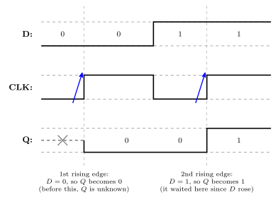
Figure 43: A D flip-flop waveform. The dashed verticals are the two rising clock edges, and the arrows mark them. Q is undefined (drawn dashed, with a cross) until the first edge. The point of the figure is the middle: D rises well before the second edge, and Q does not follow until that edge arrives.
| Clock edge | D at that edge | Q after |
|---|---|---|
| (before the first edge) | — | unknown/undefined |
| 1st rising edge | 0 | 0 |
| 2nd rising edge | 1 | 1 |
Before the first rising edge Q is undefined, because nothing has been clocked in yet; an “X” marks that stretch. Between the two rising edges Q stays 0 even though D has already risen to 1: the flip-flop is only sensitive at the edge. Remember: Q changes only when the clock (CLK) goes from 0 to 1.
A second, harder worked waveform — four clock edges, with D both rising and falling between them — is in 2026-08-10-introduction-to-sequential-circuits.
Other flip-flop types
Other types exist — JK flip-flops and T flip-flops — but they are not covered in this course. Only the D flip-flop is used.
Latches vs flip-flops
- Latches are level triggered devices — they latch the output and respond to changes of logic levels on the inputs.
- A latch circuit can be modified so that it becomes sensitive to an edge (a momentary transition) of a control input, i.e. a clock signal. Such circuits are called flip-flops.
- A flip-flop can store 1 bit of information while being sensitive to a clock edge — it changes its output only at the clock edges, based on the inputs.
- So: latches are level triggered; flip-flops are edge triggered.
A clock signal has two edges:
| Edge | Transition |
|---|---|
| Positive (rising) edge | 0 → 1 |
| Negative (falling) edge | 1 → 0 |
A D flip-flop can therefore be positive edge triggered or negative edge triggered. In a positive edge triggered D flip-flop, D is copied to Q at the positive edge of the clock; in between clock edges the flip-flop is not responsive, thus stores the value.
The state of a flip-flop is the value it is storing. Flip-flops are more useful than latches in practice.
Symbols used
Four related symbols, all drawn as a rectangle with D in at the top left, Q out at the top right, and a clock input CK at the bottom left. What distinguishes them is the marking on that CK input.
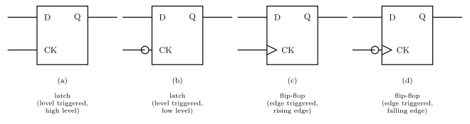
Figure 44: The four latch and flip-flop symbols, with the clock pin labelled CK (the course writes this pin CLK elsewhere). The wedge and the bubble read independently: the wedge says edge-triggered, therefore flip-flop; the bubble says inverted, therefore falling edge or low level. The reading under each symbol follows from those two rules.
| Symbol | CK input marking | Device | Triggered on |
|---|---|---|---|
| (a) | plain input | Latch | High level of CK |
| (b) | bubble (inversion circle) | Latch | Low level of CK |
| (c) | triangle/wedge | Flip-flop | Rising (positive) edge of the clock |
| (d) | bubble + triangle | Flip-flop | Falling (negative) edge of the clock |
The two markings read independently and are the whole key to the notation:
- The triangle indicates edge-triggered, and therefore that the device is a flip-flop rather than a latch. No triangle means level-triggered, i.e. a latch.
- The bubble indicates inversion, i.e. the falling edge (or the low level) rather than the rising edge (or the high level).
The SR latch (cross-coupled NOR gates)
Structure: two 2-input NOR gates cross-coupled.
- The top NOR gate takes \(S\) as one input and the bottom gate’s output as its other input; its output is \(\bar Q\).
- The bottom NOR gate takes \(R\) as one input and the top gate’s output (\(\bar Q\)) as its other input; its output is \(Q\).
So each gate’s output feeds back into the other gate’s input — that feedback loop is what stores the bit.
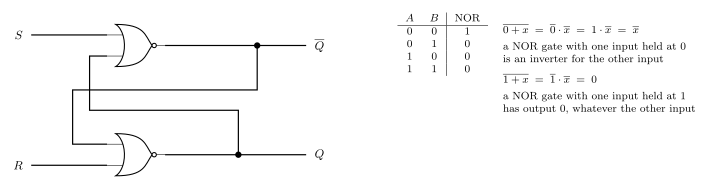
Figure 45: The SR latch: two cross-coupled NOR gates, with the NOR truth table to remember and the two special cases the analysis needs. Between them they are the whole analysis: a NOR with a 0 on one input passes the other input inverted, and a NOR with a 1 on one input is pinned to 0. Where the two feedback wires cross there is no junction dot, so it is two wires passing, not a connection.
The analysis needs both identities in the figure. Together they are what makes each row fall out in a line. Both are just De Morgan applied to a NOR (see boolean-algebra): \(\overline{A+B} = \bar A \cdot \bar B\).
The truth table:
| S | R | Q | \(\bar Q\) | Meaning |
|---|---|---|---|---|
| 0 | 0 | \(Q_{n-1}\) | — | Storage / remember |
| 0 | 1 | 0 | 1 | Reset |
| 1 | 0 | 1 | 0 | Set |
| 1 | 1 | — | — | Invalid \(\times\) |
\(Q_{n-1}\) means “whatever \(Q\) was before” — the hold row’s entry is not a bit but a reference to the previous value. Three cells are left blank: \(\bar Q\) in the hold row, and both outputs in the last row, which is Invalid.
Reasoning for each row, using the two identities above:
- \(S=0, R=0\): each gate has a 0 on its external input, so each is an inverter of the other’s output — \(\bar Q = \overline{Q}\) and \(Q = \overline{\bar Q}\). Both \(Q=1\) and \(Q=0\) satisfy that, so the latch simply holds whatever it already had. This row is the whole point of the circuit: it is the row in which the latch remembers.
- \(S=1, R=0\): the top gate has a 1 on an input, so \(\bar Q = 0\) regardless. The bottom gate then sees \(R=0\) and \(\bar Q=0\), so \(Q=1\). \(S\) sets the latch.
- \(S=0, R=1\): mirror image — the bottom gate has a 1 on an input, so \(Q=0\); the top gate then sees \(S=0\) and \(Q=0\), so \(\bar Q=1\). \(R\) resets the latch.
- \(S=1, R=1\): both gates have a 1 on an input, so both outputs are 0: \(Q = 0\) and \(\bar Q = 0\). That result is what condemns the combination: the two outputs are supposed to be complements and here they are equal, so the labels \(Q\) and \(\bar Q\) stop meaning anything. Worse, what happens after both inputs return to 0 simultaneously is not uniquely determined (the two gates race), so the resulting state is indeterminate. Hence invalid — a combination you must not apply.
This circuit is the active high SR latch: the inputs do their job when driven to 1, and the resting/hold condition is \(S=R=0\). That name is what distinguishes it from the NAND version below.
The SR latch from NAND gates (active low)
Exercise: analyse the SR latch circuit when the NOR gates are replaced with NAND gates, and complete the truth table. The answer circuit is below. The gate symbols are not merely swapped: the inputs are relabelled \(\bar S\) and \(\bar R\), and which gate’s output is called \(Q\) is swapped, so that the set/reset roles survive the change.
Figure 46: The NAND SR latch, the active low SR latch, with the NAND truth table and the two identities that drive the analysis. Compare against the NOR version: the gate outputs have swapped names, so the top gate now produces Q, and the inputs are drawn overlined because they are active low.
Worked through with the two NAND identities in the figure:
| \(\bar S\) | \(\bar R\) | Q | \(\bar Q\) | Meaning |
|---|---|---|---|---|
| 0 | 0 | 1 | 1 | Invalid — outputs not complementary |
| 0 | 1 | 1 | 0 | Set (\(\bar S\) asserted) |
| 1 | 0 | 0 | 1 | Reset (\(\bar R\) asserted) |
| 1 | 1 | \(Q_{n-1}\) | — | Storage / remember |
(Rows in ascending binary order of the inputs, which is what every truth table in the course does — see csse2010-diagram-notation.)
- \(\bar S = \bar R = 1\): each gate has a 1 on its external input, so each inverts the other’s output — the same self-consistent pair as the NOR latch’s \(S=R=0\) row. Hold.
- \(\bar S = 0\): the top gate is pinned to 1, so \(Q = 1\); the bottom gate then sees \(\bar R = 1\) and \(Q = 1\), so \(\bar Q = 0\). Set.
- \(\bar R = 0\): mirror image — \(\bar Q = 1\), and the top gate then gives \(Q = 0\). Reset.
- \(\bar S = \bar R = 0\): both gates pinned to 1, so \(Q = \bar Q = 1\). Same objection as before, so invalid.
The headline result, and the reason the inputs are drawn overlined: with NAND gates the inputs become active low. The latch rests (holds) at \(\bar S = \bar R = 1\) instead of at \(S=R=0\), and the forbidden combination moves from both-high to both-low. Everything else — set, reset, hold, one invalid corner — is the same circuit doing the same job.
This active-low convention is general: it is why the 74HCT74’s asynchronous pins are \(\overline{\text{SET}}\) and \(\overline{\text{CLR}}\) (see device-pinouts). The SET and CLR inputs are typically active low.
A real D flip-flop
A real D flip-flop is built from cross-coupled NAND gates — six NAND gates in three cross-coupled pairs: two input latches driven by D and CLK, and a third pair forming the output latch that carries \(Q\) and \(\bar Q\). That is the same storage idea as the SR latch above, wrapped in enough extra gating to make it respond to an edge rather than a level.
As well as D, CLK and the outputs \(Q\) and \(\bar Q\), it has two extra inputs:
- \(\overline{\text{PRE}}\) (Preset) — forces \(Q\) to 1.
- \(\overline{\text{CLR}}\) (Clear) — forces \(Q\) to 0.
Both are drawn with overbars and with a bubble on the pin, i.e. they are active low, and both are asynchronous: they act on the latch directly, independent of the clock, rather than waiting for a clock edge. They run straight into the NAND gates of the latches, bypassing the D/CLK path entirely — \(\overline{\text{PRE}}\) reaches the gate that produces \(Q\) and \(\overline{\text{CLR}}\) the gate that produces \(\bar Q\), which is exactly how each forces its output.
The two things to remember about these pins: they are active low inputs and asynchronous inputs.
Figure 47: The D flip-flop symbol with its asynchronous pins, CLR on top and PRE underneath. The 74HCT74 in device-pinouts is drawn the other way up (SET on top, CLR below), which is the course’s usual order; the course is also inconsistent about the naming (PRE/CLR against SET/CLR). The three consequences of the pins being asynchronous and active low are on the right.
Both pins being asserted at once (\(\overline{\text{PRE}} = \overline{\text{CLR}} = 0\)) is the same kind of contradiction as \(S=R=1\) on the NOR latch — it demands \(Q=1\) and \(Q=0\) simultaneously — and is likewise a combination to avoid. It follows from the SR-latch analysis above.
When neither is needed they can simply be omitted from a drawing: the course’s Device Pinouts and Symbols sheet says so in words, and its own logic-diagram symbol for a D flip-flop leaves them off. See device-pinouts and circuit-schematics.
D flip-flop chips
- 74HCT74 — dual D flip-flop (two independent D flip-flops in a 14-pin package), each with its own clock, its own CLR and its own PR (preset), and \(Q\)/\(\bar Q\) outputs. Pinout and schematic symbol in device-pinouts.
- 74HCT273 — eight D flip-flops in a 20-pin package, so it can hold one byte (8 bits) of information. It is not in the course’s device-symbols document, so there is no pinout for it here.
The full symbol set is in the device symbols PDF on Blackboard.
See also
- 2026-08-10-introduction-to-sequential-circuits — Lecture 5, where all of this is introduced
- sequential-circuits — what you build once you have a storage element
- shift-registers · counters · state-machines
- memory-technologies — static RAM, a memory that keeps each bit in a latch
- week3-lab-logisim-and-flip-flops — the lab that simulates these circuits
- logic-gates · boolean-algebra — the NOR/NAND behaviour the latch analysis rests on
- timing-diagrams — how to read and draw the waveforms above
- csse2010-diagram-notation — the drawing conventions these figures follow
Instruction Set Architecture
The layer where software meets hardware: what a machine instruction is, what an ISA specifies, and why assembly language exists. See cpu-organisation for the hardware below this line and avr-instructions for a real instruction set.
Machine instructions
A machine instruction is a pattern of bits. 0000 1101 0111 0111 is a valid Atmel AVR instruction. Instructions typically consist of two things:
- Opcode (operation code) — defines the operation, e.g. addition.
- Operands — what is being operated on, e.g. particular registers or a memory address.
So one word of machine code says what to do and what to do it to, packed into fixed bit fields. Which bits mean which is entirely a matter of convention — and that convention is the ISA.
The ISA
An Instruction Set Architecture is a specification — i.e. a document. It specifies the interface between hardware and software.
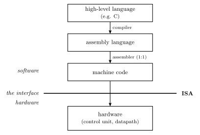
Figure 48: The ISA as an interface. Software above the line is written and compiled without knowing how the hardware works; hardware below the line is designed without knowing what program will run. The only thing both sides must agree on is which bit patterns mean what — and that agreement is a document, not a circuit.
The point of drawing it as a line is that the ISA is the only thing the two sides have to agree on. A compiler writer needs the ISA and nothing else about the chip; a chip designer needs the ISA and nothing else about the programs that will run.
Microarchitecture
Microarchitecture = the architecture of the control unit — i.e. the state machine (gates and flip-flops etc.) that implements the control unit.
This is the same state-machines material from earlier in the course, applied at the scale of a whole processor: the control unit is a state machine whose job is to emit the right control signals, in the right order, for whatever the instruction register holds.
ISA vs microarchitecture
One ISA can be implemented by many different microarchitectures. The specification says what the bit patterns mean; it does not say how a chip must go about honouring them.
| ISA | Implemented by |
|---|---|
| 8086 | many processors, in different ways |
| Pentium | Pentium … Pentium IV … Core2Duo … i7 (each in different ways), various AMD devices, and other manufacturers |
This is why a program compiled decades ago still runs: the ISA held still while the microarchitecture beneath it was rebuilt many times over.
What makes an ISA?
Four things:
- Memory models
- Registers
- Instructions
- Data types
If you know all these details, you can write machine code that runs on the CPU and build the CPU.
This is the completeness test for a specification: both sides of the line in Figure 48 have to be constructible from the document alone, and nothing else about the chip may be needed by either.
1. Memory models
How does memory look to the CPU? Four issues decide it — addressable cell size, alignment, address spaces and endianness — treated in full in memory-models.
2. Registers
Two types of register:
- General purpose — used for temporary results etc. On AVR, r0–r31.
- Special purpose, e.g.
- Program Counter (PC)
- Stack pointer (SP)
- Input/Output registers — 224 of them on the ATmega324A, see avr-io-ports
- Status register — N, Z, C, V among others. Tanenbaum calls this the Program Status Word.
Some other registers are part of the microarchitecture, NOT the ISA — e.g. the Instruction Register (IR). The programmer doesn’t need to know about these, and can’t directly change or use them.
That distinction is the cleanest illustration of what an ISA actually is. The IR unquestionably exists and holds the instruction being executed (fetch-decode-execute-cycle) — but no instruction names it, so it is invisible to software and a chip designer is free to change or remove it. The PC is the opposite case: jmp writes it, so it has to be in the specification. Existing in the hardware is not the criterion; being reachable from an instruction is.
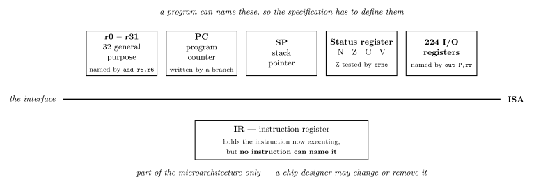
Figure 49: The same interface line as in the previous figure, with the machine’s registers sorted across it. The five above the line are part of the ISA; four of them carry an example of an instruction that names the register, and the SP box carries none. The single box below, the IR, is part of the microarchitecture only. Nothing about a register’s size or importance decides which side it lands on — only whether some instruction can refer to it.
The AVR’s own answer to this pillar — the regularity of r0–r31, the r16–r31 exception, and the X/Y/Z pointer pairs — is in avr-architecture.
3. Instructions
This is the main feature of an ISA. Instruction types include:
| Type | Does |
|---|---|
| Input/Output | communicate with I/O devices/ports |
| Load/Store | move data from/to memory |
| Move | copy data between registers |
| Arithmetic | addition, subtraction, … |
| Logical | Boolean operations |
| Branching | for deciding which instruction to perform next |
The Input/Output row is the one where the AVR’s answer is least obvious. The ATmega324A’s 224 I/O registers are all reachable by ld/st at their data-memory addresses 32 to 255 ($20 to $FF), but only the first 64 also get the short in rd, P / out P, rr form that names an I/O register by its own number P — because P is a six-bit field and \(2^6 = 64\). The other 160, the “extended” I/O registers, can only be reached the long way. The mechanics, the numbering offset and the register list are in avr-io-ports.
With arithmetic and logical merged, the same set can be cut the other way instead — by how many operands an instruction takes:
- Dyadic — two operands, one result
- Monadic — one operand, one result
And instructions use various addressing modes: how an operand says where its value is, covered in addressing-modes.
The AVR instructions met so far, sorted into these boxes, are in avr-instructions.
4. Data types
Numeric
- Integers of different lengths (8, 16, 32, 64 bits), possibly signed or unsigned
- Floating point numbers, e.g. 32 bits (single precision) or 64 bits (double precision)
- Many others not listed
Non-numeric
- Boolean (0 means false, 1 means true) — stored in a whole byte or word
- Bit-map (collection of Booleans, e.g. 8 in a byte)
- Characters
- Pointers (memory addresses)
Different machines provide hardware support for different data types. Two ends of the range:
Intel-64 Architecture
| Data type | 8 bits | 16 bits | 32 bits | 64 bits | 128 bits |
|---|---|---|---|---|---|
| Signed integer | \(\checkmark\) | \(\checkmark\) | \(\checkmark\) | \(\checkmark\) | |
| Unsigned integer | \(\checkmark\) | \(\checkmark\) | \(\checkmark\) | \(\checkmark\) | |
| BCD integer | \(\checkmark\) | ||||
| Floating point | \(\checkmark\) | \(\checkmark\) |
Atmel AVR
| Data type | 8 bits | 16 bits | 32 bits | 64 bits | 128 bits |
|---|---|---|---|---|---|
| Signed integer | \(\checkmark\) | ||||
| Unsigned integer | \(\checkmark\) | ||||
| BCD integer | |||||
| Floating point |
The only data type an AVR supports in hardware is an 8-bit integer, signed or unsigned. There is no 16-bit integer type, no floating point, no BCD.
Other data types can be supported through software! e.g. 16-bit integer operations can be built out of 8-bit operations, using a sequence of instructions — which is exactly what the two-instruction 16-bit addition in avr-instructions does. So the hardware/software line here is about cost, not possibility: anything missing from the table can still be computed, it just takes more instructions and more cycles. Floating point is the costly case: one float multiply is hundreds of instructions (floating-point-numbers), which is why fractions on the AVR are usually kept as fixed-point-numbers.
Assembly language
Machine code is too hard to program in. Assembly language is used instead:
- Human readable (just!).
- Converted into machine code by software called an assembler.
Two Atmel AVR examples:
| Assembly | Meaning |
|---|---|
add r3,r4 |
r3 ← r3 + r4 |
inc r22 |
r22 ← r22 + 1 |
The important structural detail is in the arrows of Figure 48: a high-level language compiles one-to-many — one line of C becomes however many instructions it takes — whereas assembly assembles one-to-one. Each assembly instruction is one machine instruction, written in a form a person can read. That is the whole of what an assembler buys you, and it is why assembly is still “programming the machine” in a way C is not.
The toolchain
For CSSE2010 the assembler is Microchip Studio, and two supplied tutorials walk through it end to end: Intro to Microchip Studio (create an assembler project, pick the device, edit, build, and step through the simulator) and Microchip Studio C Tutorial (the same for a GCC C project). Both are click-through guides to follow at the machine rather than material to learn — they are on Blackboard, and the labs are where they get used.
See also
- memory-models · addressing-modes — pillars 1 and 3, in full
- cpu-organisation · fetch-decode-execute-cycle · state-machines
- avr-architecture · avr-instructions · avr-io-ports · avr-program-structure
- assembly-process — what the assembler does besides translating: directives, segments and two passes · compilation-and-linking — the compiler’s one-to-many road, through object files and the linker
- 2026-08-27-avr-introduction — Lecture 10
- 2026-08-31-instruction-set-architecture-part-1 — Lecture 11
- 2026-09-03-instruction-set-architecture-part-2 — Lecture 12
The I/O Board
The I/O board in the lab kit carries the input and output devices you wire your breadboard circuits to, for experimenting with simple digital circuits. It plugs directly onto the breadboard, and adds a logic probe for debugging and a UART serial interface for talking to other devices.
It is powered from a single USB connection and has current-sense circuitry that detects short circuits and protects your designs.
Pin numbers for every device are in device-pinouts; the kit itself is loaned out in week3-lab-logisim-and-flip-flops. Two more parts of the kit that are used alongside the board, the joystick and the LED matrix, are described at the end.
What’s on it
| 1. USB connector | 2. Power LED | 3. Power switch | 4. 7-segment display |
| 5. Switches | 6. LEDs | 7. Buttons | 8. UART transmit/receive LEDs |
| 9. Logic probe indicator LEDs | 10. Fault LED | 11. VCC / GND headers | 12. I/O device headers |
| 13. Auxiliary power connector | 14. High current mode jumper |
Items 13 and 14 are the auxiliary power connector and the high-current-mode jumper. The one extra power connection the labs use is connector J1, which powers the LED matrix in Lab 16 (below).
The board at a glance
The board is a C shape: a left-hand spine carrying the USB connector, the power switch, the two status LEDs and the seven-segment display, plus a top arm and a bottom arm that straddle the breadboard’s central channel. All the I/O devices come out on the two 16-pin headers on the inner edges of those arms, and every device is reached through the column of breadboard holes directly above or below its printed label.
Figure 50: A plan view of the board, not to scale, with the parts on the left spine placed roughly. Each I/O device sits on one pin of one of the two 16-pin headers, and the column of breadboard holes at that pin is how you reach it. The board itself prints only the two end markers, a bold 32 at the left of the top header and a bold 1 at the left of the bottom one. The small numbers at the other pins are their pin numbers, the ones a schematic uses. The connection drawn in the notch is an example: switch S0 to pin 13 of a chip, LED L0 to pin 11.
Two things about the numbering are worth fixing in your head before you wire anything:
- The top header counts down, left to right. Its leftmost pin is 32 and its rightmost is 17, so the switches run
S7…S0and then the LEDsL7…L0as you read left to right. That is the opposite of the reading order you would guess from the pin numbers alone. - The bottom header counts up, left to right, pin 1 to pin 16:
TX RX CC DP G F E D C B A B3 B2 B1 B0 PR. The middle nine of those are the seven-segment display —CCits common cathode,DPits decimal point, andGdown toAits seven segments — which is why nine consecutive pins carry single-letter names.
VCC and GND pads sit at the far right of both arms, which is where the breadboard’s power rails get fed from.
Setup
Insert the board into the breadboard, aligning the downward-facing headers with the right holes.
If aligned correctly, the I/O board should not require excessive force to insert.
Connect a micro-USB cable to the connector at the top-left corner.
DO NOT STORE THE BOARD WITH THE USB CABLE ATTACHED — THIS MAY CAUSE THE USB CONNECTOR TO BREAK OFF!!
The USB connector is the part people break.
Turn the board on by sliding the PWR switch up to ON; the red power LED should light. Then check the orange FAULT LED does not light. If it does, power off immediately.
The fault LED
The board uses a current-limited power switch to protect itself and anything it powers from short circuits. A short lights the orange FAULT LED.
If it’s on: push PWR down to OFF immediately, and check your design for shorts before restoring power.
WARNING! In the case of a short circuit, the current-limiting switch may become extremely hot.
The logic probe
Attach a wire to the column of terminals above the PR label — pin 16, the rightmost pin of the bottom header. Touch the free end to any point in the circuit and the HI / LO LEDs show the logic state there.
As circuits increase in complexity, so does the necessity of having a clear strategy — probing random points in a large circuit rarely reveals the location of errors.
Suggested troubleshooting strategy
- Check the FAULT light is not on, which would indicate a short circuit.
- Probe VCC and GND at every device in your circuit, to confirm each one is actually powered.
- Start at the inputs and move logically through to the outputs. Pen and paper helps: write down the expected state at each point first, then verify it with the probe. A schematic and a truth table are great for this.
The key to any successful debugging strategy is to assume nothing, know what to expect before you begin testing, and have a plan.
Step 2 is the one worth internalising — an unpowered chip looks exactly like a wrong-logic chip until you probe its power pins, and grouped VCC/GND entries on a schematic (see circuit-schematics) make it easy to forget one.
Electrical characteristics
| VCC | 5 V |
| GND | 0 V |
| Logic high | > 3.5 V |
| Logic low | < 1.5 V |
The gap between 1.5 V and 3.5 V is undefined, which is why a floating pin can read as either (week3-lab-logisim-and-flip-flops). What the logic probe shows for a voltage inside that band is not documented.
The joystick
The kit’s two-axis joystick is a small board of its own, made to sit in the breadboard next to the I/O board. Each axis is a potentiometer between its own supply pin and ground, and the stick moves the wiper. So each axis gives a voltage that follows the stick across its travel, from 0 V at one side to 5 V at the other, for the A/D converter to read (analog-to-digital-conversion).
| Pin | What it is | Connect to |
|---|---|---|
| L/R+ | top of the left-right potentiometer | VCC |
| U/D+ | top of the up-down potentiometer | VCC |
| GND ×2 | bottom of both | GND, either one |
| L/R ×2 | x: 0 V with the stick to the left, 5 V to the right | an analog input, either one |
| U/D ×2 | y: 0 V at the bottom, 5 V at the top | an analog input, either one |
- The doubled pins are joined on the board. One wire to each of L/R, U/D and GND is enough.
- The two
+pins are separate. Both have to go to VCC, or one axis has nothing to divide. - Left, right, up and down are the joystick’s own, marked by the X and Y arrows printed on it. Placed at the right-hand end of the breadboard, with room for the microcontroller board and programmer to its left, the X arrow points to the top of the breadboard and the Y arrow to the left.
- A potentiometer’s wiper is a weak source. Anything that draws current from it, an LED for instance, pulls its voltage away from the stick’s position. LEDs make a quick wiring test, but they must come off before the converter is used.
- Keep the black foam that protects the pins when the joystick is put away.
Figure 51: The joystick’s eight pins, seen from above with the board placed as it sits in the breadboard, its X arrow pointing to the top. The pins near each corner come in twos. The dashed lines join the pins that are connected on the board itself: the two L/R pins, the two U/D pins and the two GND pins, so one wire to each pair is enough. The two supply pins, U/D+ at the top left and L/R+ at the bottom left, are not joined, and both go to VCC. L/R carries x and U/D carries y to the analog inputs.
The LED matrix
The LED matrix is a display of 16 columns by 8 rows, each pixel a red LED and a green LED together. It is driven over SPI: the AVR is the master and the matrix a slave that takes commands one byte at a time (avr-spi).
Connecting it
It has two headers:
- K1, two pins, is its power. A two-wire lead joins it to the I/O board’s connector J1, VCC on J1’s left pin and GND on its right.
- K2, four pins, is the SPI connection, to the AVR’s SPI port on PB7 to PB4: SCK on PB7, MISO on PB6, MOSI on PB5 and \(\overline{\text{SS}}\) on PB4. Match the order of the pins on K2 against the datasheet before plugging the lead in.
The Err state. PB7 to PB5 are also the pins the programmer uses to load the AVR, so programming sends the matrix a stream of what look to it like garbage commands, and it can show Err. Holding the AVR’s reset button down for at least half a second after programming clears it before the program starts.
What to send it
Every message starts with a command byte. Two commands are enough to draw anything:
| Command | Bytes | Does |
|---|---|---|
| clear | 0x0F |
every pixel off |
| set one pixel | 0x01, position, colour |
sets one pixel to a colour |
- Position byte:
(y << 4) | x. The row y, from 0 at the bottom to 7 at the top, is the high nibble. The column x, from 0 at the left to 15 at the right, is the low nibble. - Colour byte:
(green << 4) | red. Each nibble is a brightness from 0 to 15. Red alone is0x0F, green alone0xF0, both full is yellow,0xFF, and full red with half green is orange,0x7F.
The matrix’s reference manual is the full description of the commands it accepts.
Figure 52: How a pixel is addressed and coloured. The matrix is 16 columns, x from 0 to 15 left to right, by 8 rows, y from 0 to 7 bottom to top. A position byte puts y in its high nibble and x in its low one, so the pixel at x = 4, y = 2 is 0x24. A colour byte puts the green brightness in its high nibble and the red in its low one, each 0 to 15. The swatches show what some colour bytes look like: the colours here are the light from the red and green LEDs mixed.
Lab 16 works through the commands and uses them for a demo, a scrolling marquee across two matrices and an Etch-A-Sketch (week10-lab-adc-and-spi).
See also
- device-pinouts — the pin table behind Figure 50, and the board’s schematic symbols
- circuit-schematics — how the board is drawn on a schematic (
IO1/IOBOARD, input and output pentagons) - avr-io-ports — the same switches and LEDs driven from an AVR rather than from gates
- week3-lab-logisim-and-flip-flops — where the kit is loaned out
- week10-lab-adc-and-spi — Lab 16: the joystick read by the A/D converter, and the LED matrix driven over SPI
- analog-to-digital-conversion · avr-spi — the two AVR peripherals the joystick and the matrix are used with
Memory Models
The first of the four things that make up an ISA (instruction-set-architecture): how memory looks to the CPU. Four issues decide that — addressable cell size, alignment, address spaces and endianness — and every one of them is a decision the specification has to make, not something the hardware settles on its own.
Memory as addressable cells
Computer memory is conceptually a set of addressable cells:
- Each cell has a unique address (or cell number).
- Cells are usually 8 bits wide (i.e. hold one byte).
- Various cell widths have been used in the past — 8 bits is a convention, not a law.
Drawn as a table, the address indexes the rows and the cell width is how wide each row is:
| Address | ← cell width → |
|---|---|
| 0 | |
| 1 | |
| 2 | |
| 3 | |
| … |
A “4 × 3 memory” in that notation means 4 addresses of 3-bit cells — and \(4 = 2^2\), so two address bits. Built at gate level, it shows that “memory” at this level is nothing more exotic than flip-flops-and-latches and combinational-logic-blocks arranged into storage.
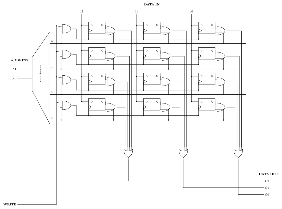
Figure 53: A 4 × 3 memory at gate level — four addresses of three-bit cells. Twelve D flip-flops in four rows of three: one row is one addressable cell. The decoder turns A1 A0 into exactly one row-select (word) line. Writing: the word line ANDed with WRITE clocks that row’s three flip-flops, so DATA IN (I2 I1 I0) — which is wired to every row’s D inputs all the time — is captured only by the selected row. Reading: each flip-flop’s Q is ANDed with its own word line and the three cells of a column are OR’d together, so the unselected rows contribute 0 and DATA OUT (O2 O1 O0) carries the selected row alone. The decoder is drawn as a trapezoid with the wide edge on the right, and the flip-flops as plain rectangles with a clock wedge on the lower-left edge, per this course’s conventions (csse2010-diagram-notation). The most significant bit, I2/O2, is the leftmost column.
A. Addressable cell size
Most common cell size is 8 bits (1 byte) — but not always.
The AVR is the counterexample sitting on the bench:
| AVR memory | Cell width |
|---|---|
| Data memory | 8 bits |
| Instruction (program) memory | 16 bits |
Which is why an AVR instruction is “one word” rather than “two bytes” — a program-memory address counts 16-bit cells.
The bus transports the content of a cell, but the data bus may be wider than one cell: it can retrieve several cells (addresses) at once. When it does, the address bus does not need to be as wide.
Bus sizes
For every doubling of the data bus width, remove the least significant bit of the address bus.
For a memory of \(2^n\) cells at 8 bits per cell — so an address size of \(n\) bits:
| Data bus | Address bus | Cells per transfer |
|---|---|---|
| 8 bits | \(n\) bits | one cell at a time |
| 16 bits | \(n-1\) bits | two cells at a time |
| 32 bits | \(n-2\) bits | four cells at a time |
The reason is that a wide transfer always moves an aligned group of cells. With a 16-bit data bus the memory only ever hands over cell pairs \((0,1), (2,3), (4,5), \dots\) — so the bottom address bit never selects anything, and naming the pair takes one bit fewer than naming the cell.
Worked example. A memory of 64 cells, 8 bits each, addressed 000000 … 111111:
\[64 = 2^6 \text{ cells} \implies 6\text{-bit addresses}\]
| Data bus | Address bus |
|---|---|
| 8 | 6 |
| 16 | 5 |
| 32 | 4 |
Read the two buses as a pair, not separately: widening one narrows the other by exactly as much.
Word addresses and byte addresses
The AVR’s 16-bit program-memory cells have one practical consequence. The program counter, jmp, call and every code label count words. But a table of constant bytes kept in flash is read a byte at a time by lpm, load program memory, and lpm takes a byte address in the Z register. Word \(w\) holds bytes \(2w\) and \(2w + 1\), with the low byte at the even address, which is the AVR being little endian (section D).
So turning a code label into a byte address means doubling it. Take the string Hello stored at word 2 by mesg: .db 72,101,108,108,111 (assembly-process):
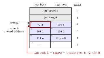
Figure 54: One region of program memory addressed two ways. Each row is a 16-bit word, numbered on the right, and each half is a byte, numbered inside its cell. The label mesg has the value 2 because labels in the code segment count words. Byte addressing counts the halves, low byte first, so word 2 starts at byte 4. That is why lpm is pointed at mesg*2: with Z = 4 it loads 72, the H. The five bytes of the string take two and a half words, and the last half word is a zero pad. Grey marks the jmp, blue the string and red the byte that lpm reads.
        ldi  ZH, high(mesg*2)   ; Z = 4: byte address of word 2
        ldi  ZL, low(mesg*2)
        lpm                     ; r0 <- 72, the H
Leaving out the *2 points Z at byte 2, the low byte of word 1, which is half of the jmp.
B. Alignment
Many architectures require natural alignment, e.g.
- 4-byte words starting at addresses 0, 4, 8, …
- 8-byte words starting at addresses 0, 8, 16, …
i.e. an \(n\)-byte value must start at an address that is a multiple of \(n\).
Taking an 8-byte word on a machine that fetches 8 bytes at a time:
| Where it sits | Reads needed | |
|---|---|---|
| Aligned | bytes 8–15, i.e. an 8-byte word at address 8 | 1 — it is exactly one fetched block |
| Non-aligned | bytes 12–19, i.e. an 8-byte word at address 12 | 2 — the top half of block 8–15, plus the bottom half of block 16–23 |
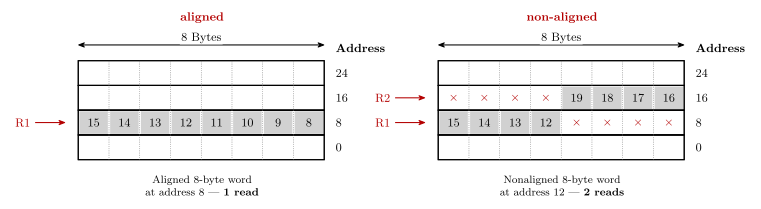
Figure 55: An aligned and a non-aligned 8-byte word. Four blocks of eight bytes; grey marks the bytes of the 8-byte word. On the left the word starts at address 8, so it is one block — one read. On the right it starts at address 12, so it takes the top half of the block at 8 and the bottom half of the block at 16 — two reads, marked R1 and R2. Two things about the drawing: addresses increase upward (unlike every other memory figure in the course, where they increase downward — see csse2010-diagram-notation on that inconsistency), and byte numbers within a row run high-to-low left to right. The × marks a byte in the fetched block that is not part of the word.
Alignment is often required because it is more efficient — the aligned case is always one read, the non-aligned case sometimes two, and the hardware that stitches two blocks together and extracts the middle is hardware that a machine demanding alignment simply does not need.
When alignment is not required — the Pentium IV
- Fetches 8 bytes at a time from memory (64-bit wide data bus).
- Alignment is NOT required, so the processor stays backwards compatible with earlier processors.
- A 4-byte word stored at address 4 takes 1 read (bytes 0 to 7).
- A 4-byte word stored at address 6 must read bytes 0 to 7 (one read) and bytes 8 to 15 (second read), then extract the 4 required bytes from the 16 bytes read.
Counting reads in general
A data bus \(w\) bytes wide delivers one aligned \(w\)-byte block per read. An \(n\)-byte value starting at address \(a\) therefore costs
\[\left\lceil \frac{(a \bmod w) + n}{w} \right\rceil \text{ reads}\]
The best case is \(n/w\) (rounded up), when the value starts on a block boundary; every other starting offset can push it one block further. So a value read from an arbitrary address costs either \(\lceil n/w \rceil\) or one more than that — which is why questions of this shape almost always answer “\(k\) or \(k+1\)” rather than a single number.
Worked example: an 8-byte value on a 16-bit data bus, no natural alignment required. Here \(w = 2\) and \(n = 8\):
| Starting address | Spans | Reads |
|---|---|---|
| Even | 4 aligned 2-byte blocks | 4 |
| Odd | 9 byte-positions, so 5 aligned blocks | 5 |
so the answer is 4 or 5. The odd case is the one to picture: one byte of the value sits alone at the top of the first block and one byte alone at the bottom of the last, and each of those still costs a whole read.
C. Address spaces
Many microprocessors have a single linear memory address space — the von Neumann architecture:
- e.g. \(2^{32}\) bytes numbered from 0 to \(2^{32} - 1\).
- (These may not be bytes — it depends on the addressable cell size.)
- Program and data share the one space.
However, the Harvard architecture has separate address spaces for instructions and data. The same numeric address means a different location depending on which space you are in, and an instruction says which one it means by what instruction it is.
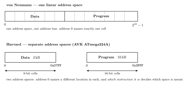
Figure 56: The two address-space models. Above: von Neumann — one linear space, so program and data are separated only by convention and address 0 names exactly one cell. Below: Harvard, in the AVR ATmega324A’s shape — two spaces, each starting at its own 0, with different sizes and different cell widths — and the cell width under each box is the whole reason the arithmetic below works out the way it does: 32 kB of program memory is \(2^{15}\) bytes but only \(2^{14}\) addresses, because each address there names a 16-bit cell. The end addresses follow from the sizes, so the data box ends at 0x07FF (\(2^{11}-1\), for 2048 bytes) rather than the 0x08FF of Figure 57, which is that 2 kB plus the 256 locations in front of it.
AVR ATmega324A is Harvard:
| Space | Size | Address width |
|---|---|---|
| Data | \(2^{11}\) (2048) bytes | 11 bits |
| Instruction | \(2^{14}\) 16-bit words — 16,384 instruction words = 32,768 bytes | 14 bits |
The arithmetic — convert to cells first, then take the logarithm:
\[\text{data: } 2\,\text{kB} = 2 \cdot 2^{10}\,\text{B} = 2^{11} \text{ cells (8-bit)} \implies 11 \text{ bits}\] \[\text{program: } 32\,\text{kB} = 2^{5} \cdot 2^{10}\,\text{B} = 2^{15}\,\text{B} = 2^{14} \text{ cells (16-bit)} \implies 14 \text{ bits}\]
The program-memory step is the one that catches people: 32 kB of flash is only \(2^{14}\) addresses, not \(2^{15}\), because each address names a 16-bit cell. Halve the byte count before taking the log whenever the cells are not bytes.
Laid out as a memory map (see avr-architecture for the rest of the chip):
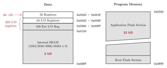
Figure 57: The ATmega324A’s two address spaces. Lowest address at the top, hex addresses outside on the right, grey fill on the coarsely-described regions, and the diagonal break across the flash meaning not to scale: that is this course’s memory-map convention (csse2010-diagram-notation). Marked in red: the register file is r0–r31, the 64 I/O plus 160 extended I/O registers are the 224 of avr-io-ports, the SRAM is 2 kB and the flash 32 kB.
Two details worth pinning down. 0x3FFF \(= 2^{14} - 1\), which is the 14 bits above. And the data space runs to 0x08FF — that is the 2 kB of SRAM plus the 256 locations (0x0000–0x00FF) that the register file and I/O registers occupy in front of it; the “\(2^{11}\) bytes” above is the SRAM itself, which is what the 11 bits size.
The assembler’s view: segments
An assembler treats each address space as a segment with its own location counter (assembly-process). On the ATmega324A there are three, because the EEPROM is a third address space alongside the two above:
| Segment | Directive | Address space | Cell | Counter starts at | The assembler can |
|---|---|---|---|---|---|
| code | .cseg |
program memory, flash, 32 kB | 16-bit word | 0x0000 |
place instructions and constants |
| data | .dseg |
data memory, SRAM | byte | 0x0100 |
only reserve space |
| EEPROM | .eseg |
EEPROM, 1 kB | byte | 0x0000 |
place constants |
Three consequences of separate spaces:
- The same number means different places. Address 0 is the reset
jmpin the code segment, registerr0in data memory and the first EEPROM byte in the EEPROM segment. - The units differ.
.org 0x0100in the code segment is word 256, which is bytes 512 and 513 of flash. In the data segment it is byte0x0100. - The data counter does not start at 0. The first 256 data addresses are the registers and I/O registers of Figure 57, so the first variable lands at
0x0100.
The data segment can only be reserved, not filled, because the assembler’s output is programmed into flash and EEPROM, which keep their contents, while SRAM starts empty at every power-up.
The memory behind each space
The three spaces are three different kinds of memory, and the kind explains how each is used (memory-technologies):
| Space | Technology | Volatile? | Erased and rewritten |
|---|---|---|---|
| Program memory | flash | no | electrically, a block at a time |
| Data memory | SRAM, flip-flops | yes | written a byte at a time, freely |
| EEPROM | EEPROM | no | electrically, one cell (byte) at a time |
The flash is divided into two blocks, the Application Flash Section and the Boot Flash Section of Figure 57. Because flash is erased a block at a time, a boot loader in the boot section can erase and rewrite the application section without erasing itself. Other AVR devices have one flash block, and some have more.
The register file and the SRAM sit at the top of the memory hierarchy. Unlike a desktop processor, the AVR has no cache: its SRAM is small enough and fast enough to keep up with the CPU directly.
D. Endianness
Different machines may support different byte orderings for a multi-byte value.
| Which end goes first (at the lowest address) | Used by | |
|---|---|---|
| Little endian | the little end — least significant byte | Intel microprocessors (Pentium etc.), and AVR |
| Big endian | the big end — most significant byte | SPARC, Freescale (formerly Motorola) microprocessors |
Most desktop/workstation/server CPUs produced since ~1992 are “bi-endian” (support both) — some switchable at boot time, others at run time, i.e. they can change dynamically.
Endianness only ever matters when a value spans more than one cell: reassembling it means knowing which cell was the low-order one.
Worked example
Given this memory:
| Address | Contents |
|---|---|
| 0 | 00001111 |
| 1 | 00110011 |
| 2 | 11011101 |
| 3 | 00101100 |
| Read | Value | Why |
|---|---|---|
| the 1-byte word at address 1 | 00110011 |
one cell — endianness does not apply |
| the 2-byte word at address 0, big endian | 00001111 00110011 |
big end first, so address 0 holds the most significant byte |
| the 2-byte word at address 2, little endian | 00101100 11011101 |
little end first, so address 2 holds the least significant byte and address 3 the most |
The mechanical way to do these without getting turned around: write the addresses the value occupies in increasing order, then assemble the answer most-significant-byte first. Big endian reads the addresses forwards; little endian reads them backwards.
See also
- instruction-set-architecture — the four pillars this is the first of
- avr-architecture — the ATmega324A’s two address spaces in full
- addressing-modes — how an instruction names a memory location
- binary-number-representations · flip-flops-and-latches · combinational-logic-blocks
- assembly-process — segments, location counters, and
.dbpacking two bytes to a word - compilation-and-linking — where a C compiler puts globals, locals and the heap in data memory
- memory-technologies — flash, SRAM and EEPROM as technologies, and why sizes are powers of 2
- memory-hierarchy-and-cache — registers, cache, main memory and disk, by speed and cost
- 2026-08-31-instruction-set-architecture-part-1 — Lecture 11 · 2026-10-08-assembly-process — Lecture 20 · 2026-10-22-memory-disks-and-files — Lecture 24
Comments and directives
Comments start with semicolons. Everything from a
;to the end of the line is ignored by the assembler..include "m324Adef.inc"is an assembler directive, not an instruction — nothing is generated for it. The contents of the file are included directly in the program, which is what makesDDRA,PORTC,TCNT0and the rest usable as names instead of I/O register numbers (see avr-io-ports). The leading dot is the giveaway: a line starting.speaks to the assembler, a line starting with a mnemonic speaks to the CPU.Every line has the same shape, with up to four fields: a label, an operation, its operands and a comment, as in
loop: jmp loop ; Repeat. The operation is either an instruction or, with the leading dot, a directive. Two more directives turn up in most programs:.def temp = r16gives a register a name, and.equgives a number a name. The fields, and every directive with what it does, are in assembly-process.