Sample Mid-semester Exam #4
exercises
exam
past-paper
computer-systems
This is the fourth of UQ’s published sample mid-semester papers for CSSE2010/CSSE7201 Introduction to Computer Systems — the Semester One 2020 St Lucia paper, run as a 60-minute open-book examination with 10 minutes of reading time. The only aids permitted are a Casio FX82-series or UQ-approved calculator; no laptops or phones. There are 25 multiple-choice questions, each worth one mark, with zero marks for an incorrect, missing or multiple answer, so there is no penalty for guessing. The course note is csse2010.
WarningAnswers are derived, not official
The source paper ships without an answer key, so every answer below was worked out during transcription rather than taken from UQ. Each one shows its reasoning so it can be checked rather than trusted; anything uncertain is flagged. Treat a disagreement between your working and the answer here as a reason to check both.
How to use this
Two ways. For a timed run, work through all 25 questions in 60 minutes without opening any of the answer callouts — on the website they stay collapsed until clicked, so the paper reads as a clean exam. For targeted practice, use the question index to pick out only the questions for one week or one concept, and read the working straight away.
Note that the PDF build renders every callout expanded, so the answers are always visible there. The site version is the one to practise from.
Question index
| Q | Topic | Week | Concept notes |
|---|---|---|---|
| 1 | Excess-64 representation | 1 | binary-number-representations |
| 2 | Radix conversion | 1 | binary-number-representations |
| 3 | Ones’ complement range | 1 | binary-number-representations |
| 4 | Properties of representations | 1 | binary-number-representations |
| 5 | Reading a gate circuit | 1 | logic-gates |
| 6 | Boolean simplification | 2 | boolean-algebra |
| 7 | Circuit for an expression | 1 | logic-gates |
| 8 | Truth table for an expression | 2 | boolean-algebra |
| 9 | Function from a timing diagram | 2 | timing-diagrams |
| 10 | NAND built from NOR gates | 2 | boolean-algebra · logic-gates |
| 11 | Equivalent expressions | 2 | boolean-algebra |
| 12 | D flip-flop input from output | 3 | flip-flops-and-latches · timing-diagrams |
| 13 | Two’s complement addition | 2 | binary-number-representations |
| 14 | Overflow detection | 2 | binary-number-representations |
| 15 | Overflow and a zero result | 2 | binary-number-representations |
| 16 | Full adder from multiplexers | 2 | combinational-logic-blocks |
| 17 | Synchronous counter sequence | 4 | counters · flip-flops-and-latches |
| 18 | Multiplexer-fed register pair | 3 | sequential-circuits · combinational-logic-blocks |
| 19 | Tracing a state machine | 4 | state-machines |
| 20 | State diagram to state table | 4 | state-machines |
| 21 | Flip-flops for a state machine | 4 | state-machines |
| 22 | Multiplexer as a logic function | 2 | combinational-logic-blocks |
| 23 | Which circuit is a latch | 3 | flip-flops-and-latches |
| 24 | ALU control settings | 5 | arithmetic-logic-unit |
| 25 | ALU operation coverage | 5 | arithmetic-logic-unit |
Q1 — Excess-64 representation
What is \(-34_{10}\) expressed in 7-bit excess-64 format?
0011110
0100010
1011101
1011110
1100010
TipAnswer
(a)
In excess-\(k\) (biased) representation the stored bit pattern is the unsigned binary of \(\text{value} + k\). Here \(k = 64\), so
\[-34 + 64 = 30\]
and \(30_{10} = 16 + 8 + 4 + 2 = 11110_2\), which padded to seven bits is \(0011110\).
A quick sanity check on the other options: \(0100010_2 = 34\), which is the unsigned 34 rather than the biased \(-34\); \(1011110_2 = 94 = 30 + 64\), i.e. the pattern you get if you add the bias twice. See binary-number-representations.
Q2 — Radix conversion
\(95_{16}\) is equal to
\(10100101_2\)
\(137_8\)
\(141_{10}\)
\(225_8\)
None of the above
TipAnswer
(d)
\(95_{16} = 9 \times 16 + 5 = 149_{10}\). In binary that is \(1001\,0101_2\) (each hex digit expands to four bits: \(9 \to 1001\), \(5 \to 0101\)).
Regrouping those bits in threes from the right for octal: \(010\;010\;101 \to 225_8\). Checking: \(2 \times 64 + 2 \times 8 + 5 = 128 + 16 + 5 = 149\). ✓
The distractors are all near misses: \(10100101_2 = 165\), \(137_8 = 95\) (the digits of the hex number read as a decimal value), and \(141_{10}\) is simply wrong.
Q3 — Ones’ complement range
A 4-bit number in ones’ complement format can represent integers from
-15 to 15
-8 to 7
-7 to 7
-7 to 8
0 to 15
TipAnswer
(c)
In ones’ complement the negative of a value is its bit-by-bit complement, so the positive patterns \(0000 \ldots 0111\) cover \(0 \ldots 7\) and their complements \(1111 \ldots 1000\) cover \(-0 \ldots -7\). The range is therefore \(-7\) to \(+7\), with two representations of zero (\(0000\) and \(1111\)) — which is exactly why ones’ complement has one fewer distinct value than two’s complement’s \(-8\) to \(+7\) (option (b)). See binary-number-representations.
Q4 — Properties of representations
Which of the following statements about number representations is false?
The 8-bit number 01100110 is even when considered to be in unsigned, signed-magnitude, ones’ complement, two’s complement or excess-128 formats
An n-bit excess \(2^{n-1}\) number can be converted to two’s complement representation by inverting the most significant bit
An 8-bit ones’ complement number can be converted to 9-bit ones’ complement representation by prepending a copy of the most significant bit
An 8-bit two’s complement number can be converted to 9-bit two’s complement representation by prepending a copy of the most significant bit
None of the above
TipAnswer
(e)
All four statements are true, so the answer is “none of the above”.
(a) \(01100110\) has a 0 in the least significant bit. Unsigned it is \(102\); as signed-magnitude the sign bit is 0 so it is \(+102\); in ones’ complement and two’s complement the leading 0 again means \(+102\); in excess-128 it is \(102 - 128 = -26\). All five values are even. (Parity of the interpreted value is really just the LSB in the first four formats, and biasing by the even number 128 cannot change parity either.)
(b) For an \(n\)-bit excess-\(2^{n-1}\) number the stored pattern is \(v + 2^{n-1}\), and in two’s complement it is \(v \bmod 2^n\). Adding \(2^{n-1}\) modulo \(2^n\) flips exactly the most significant bit and leaves the rest alone, so inverting the MSB converts between the two.
(c) and (d) are both sign extension. Copying the sign bit preserves the value in ones’ complement (\(-3 = 11111100 \to 111111100\), still the complement of \(000000011\)) and in two’s complement (\(-3 = 11111101 \to 111111101 = 512 - 3\)). Only unsigned and signed-magnitude would break under this rule.
Q5 — Reading a gate circuit
What function is implemented by the following circuit?
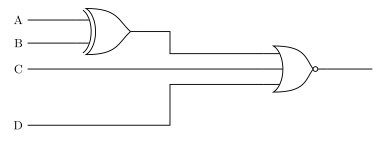
Figure 1: Question 5’s circuit: an XOR on A and B feeding a three-input NOR together with C and D.
\((A \oplus B) + C + D\)
\(\overline{A \oplus B} + \overline{C} + \overline{D}\)
\(\overline{(A \oplus B) + (C + D)}\)
\((A \oplus B) . \overline{C} . \overline{D}\)
\(\overline{\overline{A \oplus B} . (C + D)}\)
TipAnswer
(c)
Read it left to right. The first gate has the extra curved bar across its inputs, so it is an XOR: its output is \(A \oplus B\). The second gate has the same curved back but a bubble on its output and three inputs, so it is a three-input NOR fed by \(A \oplus B\), \(C\) and \(D\):
\[X = \overline{(A \oplus B) + C + D}\]
Option (c) is that expression with \(C + D\) merely bracketed, and OR is associative, so (c) is the same function.
The near misses are worth checking. Option (a) drops the inversion. Option (b), \(\overline{A \oplus B} + \overline{C} + \overline{D}\), is by De Morgan \(\overline{(A \oplus B) . C . D}\) — the three-input NAND, not the NOR. Option (d) has the right form for De Morgan applied to (c) except that the first term is not inverted; the correct expansion is \(\overline{A \oplus B} . \overline{C} . \overline{D}\). Option (e) inverts the wrong subexpression.
Q6 — Boolean simplification
Which of the following logic functions is identical to \(\overline{\overline{\overline{A + B} + C} + \overline{B . C}}\) ?
0
\(B . C\)
\(A . B . C\)
\(\overline{B} + \overline{C}\)
None of the above
TipAnswer
(b)
The bars in the printed expression nest three deep on the left-hand term: innermost \(\overline{A + B}\), then \(\overline{\overline{A + B} + C}\), and the whole thing is NORed with \(\overline{B . C}\).
Name the two operands of the outer bar \(P = \overline{\overline{A+B} + C}\) and \(R = \overline{B.C}\), so the function is \(\overline{P + R}\). By De Morgan that is \(\overline{P} . \overline{R}\), and both complements collapse a level of bars:
\[ \begin{aligned} \overline{P} &= \overline{A + B} + C \\ \overline{R} &= B . C \end{aligned} \]
so
\[ \begin{aligned} X &= \left( \overline{A + B} + C \right) . B . C \\ &= \left( \overline{A} . \overline{B} + C \right) . B . C && \text{(De Morgan)} \\ &= \overline{A} . \overline{B} . B . C + C . B . C && \text{(distribute)} \\ &= 0 + B . C && \text{($\overline{B} . B = 0$, $C . C = C$)} \\ &= B . C \end{aligned} \]
The \(\overline{B} . B\) term is what kills the \(A\) dependence, which is why the answer has no \(A\) in it at all. See boolean-algebra.
Q7 — Circuit for an expression
Which of the following logic circuits is an implementation of the function \((A \oplus B) + C + \overline{D}\)?
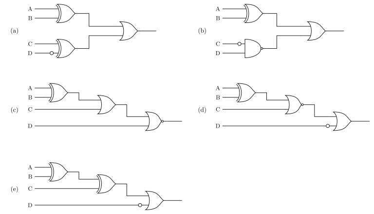
Figure 2: Question 7’s five candidate circuits, drawn side by side as in the paper. Small open circles on an input or output lead are inversion bubbles.
TipAnswer
(b)
The target is an OR of three terms: \(A \oplus B\), \(C\), and \(\overline{D}\). Every candidate starts with \(A \oplus B\), so the question is what the rest of each circuit does with \(C\) and \(D\).
In (b) the lower gate is an AND with a bubble on its output (a NAND) and a bubble on its \(C\) input, so it computes \(\overline{\overline{C} . D}\). De Morgan turns that into \(C + \overline{D}\), and the final OR adds \(A \oplus B\):
\[(A \oplus B) + \left(C + \overline{D}\right) = (A \oplus B) + C + \overline{D} \quad ✓\]
The others fail:
- (a) the lower gate is an XOR, giving \((A \oplus B) + (C \oplus \overline{D})\). Try \(C = 1, D = 0\): the target is 1 but \(C \oplus \overline{D} = 1 \oplus 1 = 0\), so the two differ whenever \(A \oplus B = 0\).
- (c) ends in a NOR, so the whole result is inverted: \(\overline{(A \oplus B) + C + D}\).
- (d) is \(\overline{(A \oplus B) + C} + \overline{D}\) — the NOR is in the middle, so the first two terms come out inverted.
- (e) cascades XORs: \(\left((A \oplus B) \oplus C\right) + \overline{D}\), which is not the same as ORing \(C\) in.
Q8 — Truth table for an expression
Which of the following truth tables is equivalent to the function \(X = (A . \overline{B} + C) . \overline{(B + A . \overline{C})}\)
| A | B | C | X |
|---|---|---|---|
| 0 | 0 | 0 | 1 |
| 0 | 0 | 1 | 1 |
| 0 | 1 | 0 | 0 |
| 0 | 1 | 1 | 0 |
| 1 | 0 | 0 | 0 |
| 1 | 0 | 1 | 0 |
| 1 | 1 | 0 | 0 |
| 1 | 1 | 1 | 0 |
| A | B | C | X |
|---|---|---|---|
| 0 | 0 | 0 | 1 |
| 0 | 0 | 1 | 1 |
| 0 | 1 | 0 | 0 |
| 0 | 1 | 1 | 0 |
| 1 | 0 | 0 | 0 |
| 1 | 0 | 1 | 1 |
| 1 | 1 | 0 | 0 |
| 1 | 1 | 1 | 0 |
| A | B | C | X |
|---|---|---|---|
| 0 | 0 | 0 | 0 |
| 0 | 0 | 1 | 1 |
| 0 | 1 | 0 | 0 |
| 0 | 1 | 1 | 0 |
| 1 | 0 | 0 | 0 |
| 1 | 0 | 1 | 0 |
| 1 | 1 | 0 | 0 |
| 1 | 1 | 1 | 0 |
| A | B | C | X |
|---|---|---|---|
| 0 | 0 | 0 | 0 |
| 0 | 0 | 1 | 1 |
| 0 | 1 | 0 | 0 |
| 0 | 1 | 1 | 0 |
| 1 | 0 | 0 | 0 |
| 1 | 0 | 1 | 1 |
| 1 | 1 | 0 | 0 |
| 1 | 1 | 1 | 0 |
- None of the above
TipAnswer
(d)
Evaluate the two factors separately. Write \(P = A . \overline{B} + C\) and \(Q = \overline{B + A . \overline{C}}\), so \(X = P . Q\):
| A | B | C | \(A.\overline{B}\) | \(P\) | \(A.\overline{C}\) | \(B + A.\overline{C}\) | \(Q\) | \(X\) |
|---|---|---|---|---|---|---|---|---|
| 0 | 0 | 0 | 0 | 0 | 0 | 0 | 1 | 0 |
| 0 | 0 | 1 | 0 | 1 | 0 | 0 | 1 | 1 |
| 0 | 1 | 0 | 0 | 0 | 0 | 1 | 0 | 0 |
| 0 | 1 | 1 | 0 | 1 | 0 | 1 | 0 | 0 |
| 1 | 0 | 0 | 1 | 1 | 1 | 1 | 0 | 0 |
| 1 | 0 | 1 | 1 | 1 | 0 | 0 | 1 | 1 |
| 1 | 1 | 0 | 0 | 0 | 1 | 1 | 0 | 0 |
| 1 | 1 | 1 | 0 | 1 | 0 | 1 | 0 | 0 |
\(X\) is 1 for \(ABC = 001\) and \(101\) only, which is table (d). Note that \(Q\) forces \(X = 0\) whenever \(B = 1\), so only the four \(B = 0\) rows can ever be 1, and of those the two with \(C = 0\) fail — at \(000\) because \(P = 0\), and at \(100\) because \(A.\overline{C} = 1\) makes \(Q = 0\).
Simplified, \(X = \overline{B} . C\), which is a neater way to check the table.
Q9 — Function from a timing diagram
What logic function does the following timing diagram represent?
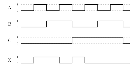
Figure 3: Question 9’s timing diagram. A, B and C step through all eight input combinations with A as the fastest signal, and X is the output to be identified.
\(A \oplus B \oplus C\)
\(A . \overline{B} . \overline{C} + \overline{A} . B . \overline{C} + \overline{A} . \overline{B} . C\)
\(A . B . \overline{C} + A . \overline{B} . C + \overline{A} . B . C\)
\(A . \overline{B} . \overline{C} + \overline{A} . B . C + \overline{A} . \overline{B} . C\)
None of the above
TipAnswer
(b)
A timing diagram is a truth table drawn sideways (see timing-diagrams). Reading the eight time slots left to right, \(A\) toggles every slot, \(B\) every two and \(C\) every four, so the slots walk through all eight combinations with \(A\) as the least significant bit:
| Slot | A | B | C | X |
|---|---|---|---|---|
| 0 | 0 | 0 | 0 | 0 |
| 1 | 1 | 0 | 0 | 1 |
| 2 | 0 | 1 | 0 | 1 |
| 3 | 1 | 1 | 0 | 0 |
| 4 | 0 | 0 | 1 | 1 |
| 5 | 1 | 0 | 1 | 0 |
| 6 | 0 | 1 | 1 | 0 |
| 7 | 1 | 1 | 1 | 0 |
\(X\) is 1 in exactly the three slots where precisely one input is 1, so as a sum of minterms
\[X = A . \overline{B} . \overline{C} + \overline{A} . B . \overline{C} + \overline{A} . \overline{B} . C\]
which is option (b) — an “exactly one input is high” detector.
Option (a) is tempting because \(A \oplus B \oplus C\) is also 1 for those three combinations, but three-input XOR is odd parity, so it is 1 for \(ABC = 111\) as well, and the diagram shows \(X = 0\) there. Options (c) and (d) each pick the wrong three minterms.
Q10 — NAND built from NOR gates
Which of the following circuits implements a 3 input NAND gate (\(\overline{A . B . C}\)) using only 2-input NOR gates?
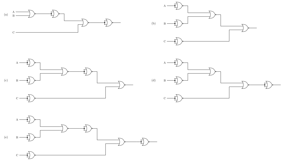
Figure 4: Question 10’s five candidate NOR-only circuits. A NOR gate with both inputs tied together (marked by a junction dot) is being used as an inverter.
TipAnswer
(e)
The target is \(\overline{A.B.C} = \overline{A} + \overline{B} + \overline{C}\). A NOR with its inputs tied together is an inverter, since \(\overline{x + x} = \overline{x}\), and a NOR of two inverted signals is an AND, since \(\overline{\overline{x} + \overline{y}} = x . y\). Those two facts decide every option.
Working each circuit through:
(a) \(\overline{A+B}\), inverted back to \(A + B\), NORed with \(C\) to give \(\overline{A+B+C}\), then inverted again: the output is \(A + B + C\).
(b) \(\overline{A}\), \(\overline{B}\), \(\overline{C}\); then \(\overline{\overline{A} + \overline{B}} = A.B\); then \(\overline{A.B + \overline{C}} = \overline{A.B} . C\). At \(A = B = C = 0\) this gives 0, but the NAND should give 1.
(c) the same up to \(A.B\), then an inverter making \(\overline{A.B}\), then \(\overline{\overline{A.B} + \overline{C}} = A.B.C\) — the AND, not the NAND.
(d) \(A.B\), then \(\overline{A.B + \overline{C}} = \overline{A.B}.C\), then an inverter giving \(A.B + \overline{C}\). At \(A = B = C = 1\) that is 1, but the NAND should give 0.
(e) \(A.B\), invert to \(\overline{A.B}\), NOR with \(\overline{C}\) to get \(\overline{\overline{A.B} + \overline{C}} = A.B.C\), then invert once more:
\[\overline{A.B.C} \quad ✓\]
Circuit (e) is (c) with one extra inverter on the end, which is exactly the difference between AND and NAND — worth noticing, because (c) is the obvious trap.
Q11 — Equivalent expressions
Consider the logic function represented by the following truth table:
| A | B | C | X |
|---|---|---|---|
| 0 | 0 | 0 | 1 |
| 0 | 0 | 1 | 1 |
| 0 | 1 | 0 | 1 |
| 0 | 1 | 1 | 0 |
| 1 | 0 | 0 | 1 |
| 1 | 0 | 1 | 1 |
| 1 | 1 | 0 | 0 |
| 1 | 1 | 1 | 0 |
Which of the following expressions is NOT equivalent to this function?
\(\overline{B} + \overline{A} . \overline{C}\)
\(\overline{A} . \overline{B} + \overline{A} . \overline{C} + A . \overline{B}\)
\(\overline{A} . \overline{B} . \overline{C} + \overline{B}\)
\(\overline{B} . C + \overline{A} . \overline{C} + \overline{B} . \overline{C}\)
\(\overline{A} . \overline{B} . \overline{C} + \overline{A} . B . \overline{C} + A . \overline{B} . \overline{C} + \overline{A} . \overline{B} . C + A . \overline{B} . C\)
TipAnswer
(c)
First get a canonical form. \(X = 1\) on the rows \(000\), \(001\), \(010\), \(100\), \(101\). Grouping the four rows with \(B = 0\) collapses them completely, leaving one extra term for row \(010\):
\[ \begin{aligned} X &= \overline{A}.\overline{B}.\overline{C} + \overline{A}.\overline{B}.C + A.\overline{B}.\overline{C} + A.\overline{B}.C + \overline{A}.B.\overline{C} \\ &= \overline{B} + \overline{A}.B.\overline{C} && \text{(the four $B=0$ rows are all of $\overline{B}$)} \\ &= \overline{B} + \overline{A}.\overline{C} && \text{($x + \overline{x}y = x + y$ with $x = \overline{B}$)} \end{aligned} \]
So the function is \(\overline{B} + \overline{A}.\overline{C}\), which is option (a) verbatim. Checking the rest:
- (b) \(\overline{A}.\overline{B} + A.\overline{B} = \overline{B}\), leaving \(\overline{B} + \overline{A}.\overline{C}\). Equivalent.
- (c) \(\overline{A}.\overline{B}.\overline{C}\) is contained in \(\overline{B}\), so by absorption the whole expression is just \(\overline{B}\). That loses row \(010\) (\(A=0\), \(B=1\), \(C=0\)), where the table says \(X = 1\) but \(\overline{B} = 0\). Not equivalent — this is the answer.
- (d) \(\overline{B}.C + \overline{B}.\overline{C} = \overline{B}(C + \overline{C}) = \overline{B}\), leaving \(\overline{B} + \overline{A}.\overline{C}\). Equivalent.
- (e) is the sum of exactly the five minterms where \(X = 1\). Equivalent by construction.
Q12 — D flip-flop input from output
Consider the flip-flop circuit shown below and the associated CLK and output (Q) signals. Which timing diagram shows input (A) values over time which would have resulted in the given output (Q).
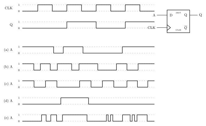
Figure 5: Question 12’s given CLK and Q waveforms and the positive-edge-triggered D flip-flop that produced them, with the five candidate A waveforms below.
TipAnswer
(e)
The triangle on the clock input makes this a positive-edge-triggered D flip-flop, so the only thing that matters is the value of A at the instant of each rising clock edge; everything A does between edges is invisible. There are four rising edges in the diagram, and Q tells us what A must have been at each:
| Rising edge | Q after the edge | so A at the edge |
|---|---|---|
| 1st | 0 (unchanged) | 0 |
| 2nd | 1 | 1 |
| 3rd | 0 | 0 |
| 4th | 1 | 1 |
So A must read 0, 1, 0, 1 at the four rising edges. Checking each candidate at those four instants:
- (a) is high at the first rising edge — needs 0. ✗
- (b) gives 0, 1, 1, … — wrong at the third edge, where its pulse has not yet fallen. ✗
- (c) gives 0, 0, … — it is low across the second rising edge. ✗
- (d) gives 0, 1, 0, 0 — its single pulse has long finished by the fourth edge. ✗
- (e) gives 0, 1, 0, 1 at the four edges. ✓
Waveform (e) is deliberately full of narrow glitches, and that is the point of the question: none of them land on a rising clock edge, so the flip-flop never sees them. See flip-flops-and-latches.
Q13 — Two’s complement addition
What’s the result of adding the 6-bit two’s complement numbers 101101 and 110011?
000000
010000
100000
111110
111111
TipAnswer
(c)
Add the bit patterns as plain binary and discard the carry out of the top bit, which is what two’s complement addition amounts to:
    101101
  + 110011
  --------
  1 100000
Every column from the least significant up produces a carry, and the carry out of the top bit is dropped, so the result in six bits is \(100000\).
Checking in decimal: \(101101\) has its MSB set, so its magnitude is the two’s complement \(\overline{101101} + 1 = 010010 + 1 = 010011 = 19\), i.e. the value is \(-19\). Likewise \(110011 \to 001100 + 1 = 001101 = 13\), i.e. \(-13\). The sum is \(-32\), and \(-32\) in 6-bit two’s complement is \(100000\). ✓
Two negatives adding to a negative means no overflow, so the six-bit answer is valid. See binary-number-representations, and Beyond the paper below for the single chip that does this addition in hardware — the same chip whether you read the operands as signed or unsigned.
Q14 — Overflow detection
Which of the following operations will result in an overflow in 6-bit two’s complement arithmetic?
011111 – 010010
101011 – 111000
110100 – 000111
010101 + 111111
None of the above
TipAnswer
(e)
Six-bit two’s complement covers \(-32\) to \(+31\). Overflow happens exactly when the true mathematical result falls outside that window, so convert each operand and check:
| operands (decimal) | result | in range? | |
|---|---|---|---|
| (a) | \(011111 = 31\), \(010010 = 18\) | \(31 - 18 = 13\) | yes |
| (b) | \(101011 = -21\), \(111000 = -8\) | \(-21 - (-8) = -13\) | yes |
| (c) | \(110100 = -12\), \(000111 = 7\) | \(-12 - 7 = -19\) | yes |
| (d) | \(010101 = 21\), \(111111 = -1\) | \(21 + (-1) = 20\) | yes |
None of them overflows, so the answer is (e).
The structural shortcut gets there faster in three of the four cases: subtracting two values of the same sign, or adding two values of opposite sign, can never overflow, because the result lies between the two operands. That immediately clears (a) (positive minus positive), (b) (negative minus negative) and (d) (positive plus negative). Only (c) — negative minus positive — can overflow in principle, and \(-19\) comfortably fits.
The same decision made in gates, from the sign bits of the operands and of the result, is the overflow LED of Beyond the paper below.
Q15 — Overflow and a zero result
Consider the binary addition operation 1010 + 0110. Which of the following statements is true if the numbers are interpreted as two’s complement?
The result is negative and no overflow occurs
The result should be negative but overflow occurs
The result is positive and no overflow occurs
The result should be positive but overflow occurs
The result is zero
TipAnswer
(e)
As 4-bit two’s complement, \(1010\) has its sign bit set so its magnitude is \(\overline{1010} + 1 = 0101 + 1 = 0110 = 6\), i.e. the value is \(-6\); and \(0110 = +6\). The sum is \(-6 + 6 = 0\).
The bit-level addition agrees:
  1010
+ 0110
------
 10000
The carry out of the top bit is discarded, leaving \(0000\). Note that the carry out being 1 does not mean overflow here — for two’s complement, overflow is signalled by the carry into the sign bit differing from the carry out of it, and here both are 1. Adding a positive and a negative number can never overflow anyway, since the result always lies between them.
So the result is exactly zero, which is neither the “negative” of (a) nor the “positive” of (c), and no overflow occurs, ruling out (b) and (d).
On the board this is two lit indicators that mean opposite things: the carry-out LED on and the overflow LED off. Beyond the paper below shows why they are separate outputs.
Q16 — Full adder from multiplexers
Consider the full-adder shown below:
In the multiplexer circuit below, what values do the multiplexer inputs X0,X1,X2,X3 and Y0,Y1,Y2,Y3 need to take on in order for the circuit to implement a full-adder?
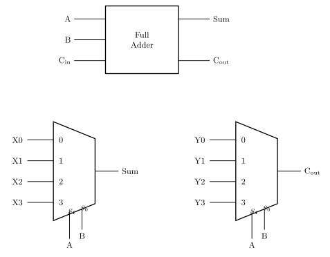
Figure 6: Question 16’s full-adder block and the two 4-to-1 multiplexers that are to implement it, with A on the \(S_1\) select and B on \(S_0\).
X0 = 0, X1 = 1, X2 = 1, X3 = 0; Y0 = 0, Y1 = 0, Y2 = 0, Y3 = 1
X0 = \(C_{in}\), X1 = \(\overline{C_{in}}\), X2 = \(\overline{C_{in}}\), X3 = \(C_{in}\); Y0 = 0, Y1 = \(C_{in}\), Y2 = \(C_{in}\), Y3 = 1
X0 = 0, X1 = \(\overline{C_{in}}\), X2 = \(\overline{C_{in}}\), X3 = 1; Y0 = 0, Y1 = \(C_{in}\), Y2 = \(C_{in}\), Y3 = 1
X0 = \(C_{in}\), X1 = 1, X2 = 1, X3 = \(C_{in}\); Y0 = 0, Y1 = \(\overline{C_{in}}\), Y2 = \(\overline{C_{in}}\), Y3 = \(C_{in}\)
None of the above
TipAnswer
(b)
Both multiplexers are steered by the same select pair, \(S_1 = A\) and \(S_0 = B\), so input \(n\) of each multiplexer is the one selected when \(AB\) is the two-bit number \(n\). Each data input therefore has to be the full-adder output as a function of \(C_{in}\) alone, for that one combination of A and B. This is the standard “multiplexer as a function generator” trick — see combinational-logic-blocks.
The full adder is \(\text{Sum} = A \oplus B \oplus C_{in}\) and \(\text{C}_{out} = A.B + C_{in}.(A \oplus B)\), so:
| \(S_1 S_0 = AB\) | input | \(A \oplus B\) | Sum \(= (A \oplus B) \oplus C_{in}\) | \(C_{out}\) |
|---|---|---|---|---|
| 00 | X0 / Y0 | 0 | \(C_{in}\) | 0 |
| 01 | X1 / Y1 | 1 | \(\overline{C_{in}}\) | \(C_{in}\) |
| 10 | X2 / Y2 | 1 | \(\overline{C_{in}}\) | \(C_{in}\) |
| 11 | X3 / Y3 | 0 | \(C_{in}\) | 1 |
That is exactly option (b). The pattern is easy to remember: the Sum multiplexer gets \(C_{in}\) where \(A \oplus B = 0\) and \(\overline{C_{in}}\) where \(A \oplus B = 1\); the carry multiplexer gets the constants 0 and 1 where A and B agree, and \(C_{in}\) where they differ.
This is one bit slice. Four of them chained carry-to-carry are what a 74HCT283 holds in a single package — see Beyond the paper below.
Q17 — Synchronous counter sequence
What sequence will the following synchronous counter count through, if it starts at \(Q_1Q_0 = 00\)?
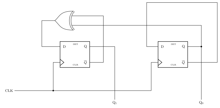
Figure 7: Question 17’s counter. Note which flip-flop output feeds the XOR: the wire from FF1’s \(\overline{Q}\) turns up to the gate, while FF1’s Q crosses it and carries on to the \(Q_1\) label.
\(Q_1Q_0\): \(00 \to 11 \to 10 \to 01 \to 00 \to \ldots\)
\(Q_1Q_0\): \(00 \to 11 \to 10 \to 11 \to 10 \to \ldots\)
\(Q_1Q_0\): \(00 \to 01 \to 10 \to 11 \to 00 \to \ldots\)
\(Q_1Q_0\): \(00 \to 01 \to 00 \to \ldots\)
\(Q_1Q_0\): \(00 \to 11 \to 00 \to \ldots\)
TipAnswer
(a)
Read the excitation equations off the wiring. The right-hand flip-flop has its own \(\overline{Q}\) routed back round to its D input, so it toggles every clock:
\[D_0 = \overline{Q_0}\]
The XOR feeding the left-hand flip-flop takes \(Q_0\) along the long top wire and — this is the detail the question turns on — \(\overline{Q_1}\), not \(Q_1\): the wire that turns up into the gate leaves FF1’s \(\overline{Q}\) pin, and FF1’s Q wire merely crosses it on its way to the \(Q_1\) output. So
\[D_1 = Q_0 \oplus \overline{Q_1}\]
Both flip-flops share CLK, so the counter is synchronous and both update from the current state. Tracing from \(Q_1Q_0 = 00\):
| \(Q_1 Q_0\) | \(D_1 = Q_0 \oplus \overline{Q_1}\) | \(D_0 = \overline{Q_0}\) | next |
|---|---|---|---|
| 00 | \(0 \oplus 1 = 1\) | 1 | 11 |
| 11 | \(1 \oplus 0 = 1\) | 0 | 10 |
| 10 | \(0 \oplus 0 = 0\) | 1 | 01 |
| 01 | \(1 \oplus 1 = 0\) | 0 | 00 |
So \(00 \to 11 \to 10 \to 01 \to 00 \to \ldots\), which is option (a) — a down-counter.
Had the XOR been fed \(Q_1\) instead, \(D_1\) would be \(Q_1 \oplus Q_0\) and the sequence would be the ordinary up-count \(00 \to 01 \to 10 \to 11\) of option (c), so the two answers differ by exactly which flip-flop pin that wire leaves from. See counters.
Q18 — Multiplexer-fed register pair
Consider the circuit below. If \(A_1\) is 0 and \(A_0\) is 1, what are the values of \(Q_1\) and \(Q_0\) after four rising clock edges if FN is 0 for one rising clock edge then 1 for three rising clock edges?
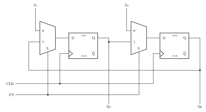
Figure 8: Question 18’s circuit: each flip-flop is fed by a 2-to-1 multiplexer that selects between an external input and the other flip-flop’s output, under the common FN control.
\(Q_1 = 0\), \(Q_0 = 0\)
\(Q_1 = 0\), \(Q_0 = 1\)
\(Q_1 = 1\), \(Q_0 = 0\)
\(Q_1 = 1\), \(Q_0 = 1\)
Insufficient information is provided to determine the values
TipAnswer
(c)
Both multiplexers share the select line FN, and each takes the external input on its “0” leg and the other flip-flop’s output on its “1” leg — \(Q_0\) comes back along the bottom rail into the left multiplexer, and \(Q_1\) crosses over into the right one. So
\[ \begin{aligned} D_1 &= \begin{cases} A_1 & \text{FN} = 0 \\ Q_0 & \text{FN} = 1 \end{cases} &\qquad D_0 &= \begin{cases} A_0 & \text{FN} = 0 \\ Q_1 & \text{FN} = 1 \end{cases} \end{aligned} \]
FN = 0 is a parallel load of \(A_1A_0\); FN = 1 swaps the two bits. With \(A_1 = 0\), \(A_0 = 1\):
| Edge | FN | \(Q_1 Q_0\) after |
|---|---|---|
| 1 | 0 | \(01\) (load \(A_1A_0\)) |
| 2 | 1 | \(10\) (swap) |
| 3 | 1 | \(01\) (swap) |
| 4 | 1 | \(10\) (swap) |
After the fourth edge \(Q_1 = 1\) and \(Q_0 = 0\), which is option (c). Note that the initial contents of the flip-flops never matter, because the first edge loads them both — so (e) is wrong.
Q19 — Tracing a state machine
Consider the state machine represented by the state diagram below:
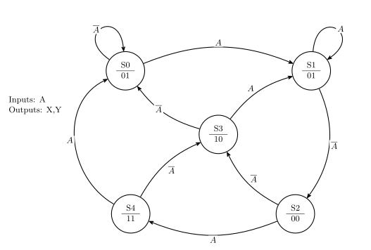
Figure 9: Question 19’s five-state machine. Each circle carries the state name above the rule and its X,Y output below.
What sequence of states is traversed if the machine starts in state S1 and A goes through the sequence 101010101?
S1\(\to\)S2\(\to\)S4\(\to\)S3\(\to\)S1\(\to\)S2\(\to\)S4\(\to\)S3\(\to\)S1\(\to\)S2
S1\(\to\)S1\(\to\)S2\(\to\)S3\(\to\)S1\(\to\)S2\(\to\)S4\(\to\)S3\(\to\)S1\(\to\)S2
S1\(\to\)S1\(\to\)S2\(\to\)S4\(\to\)S3\(\to\)S1\(\to\)S2\(\to\)S4\(\to\)S3\(\to\)S1
S1\(\to\)S1\(\to\)S2\(\to\)S4\(\to\)S0\(\to\)S0\(\to\)S1\(\to\)S2\(\to\)S4\(\to\)S3
None of the above
TipAnswer
(c)
First read the transitions off the diagram:
| State | on \(\overline{A}\) | on \(A\) |
|---|---|---|
| S0 | S0 | S1 |
| S1 | S2 | S1 |
| S2 | S3 | S4 |
| S3 | S0 | S1 |
| S4 | S3 | S0 |
Now walk the input \(1,0,1,0,1,0,1,0,1\) from S1, listing the starting state and then the state after each input:
\[\mathrm{S1} \xrightarrow{1} \mathrm{S1} \xrightarrow{0} \mathrm{S2} \xrightarrow{1} \mathrm{S4} \xrightarrow{0} \mathrm{S3} \xrightarrow{1} \mathrm{S1} \xrightarrow{0} \mathrm{S2} \xrightarrow{1} \mathrm{S4} \xrightarrow{0} \mathrm{S3} \xrightarrow{1} \mathrm{S1}\]
Ten states for nine inputs, which is option (c). The machine falls into the four-state loop S1 → S2 → S4 → S3 → S1 and never visits S0 for this input, because S0 is only reachable from S3 on \(\overline{A}\) or S4 on \(A\), and neither happens here.
Option (a) is the same walk with the first (self-loop) step omitted, so it is the trap for forgetting that the initial 1 leaves the machine in S1. See state-machines.
Q20 — State diagram to state table
Consider the state diagram below.
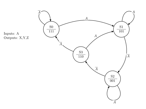
Figure 10: Question 20’s four-state machine, with each state’s X,Y,Z output printed under its name.
Which of the following is an equivalent state table?
| Current State | Input (A) | Next State | Outputs (X,Y,Z) |
|---|---|---|---|
| S0 | 0 | S0 | 111 |
| S0 | 1 | S1 | 111 |
| S1 | 0 | S1 | 101 |
| S1 | 1 | S2 | 101 |
| S2 | 0 | S3 | 001 |
| S2 | 1 | S2 | 001 |
| S3 | 0 | S0 | 110 |
| S3 | 1 | S1 | 110 |
| Current State | Input (A) | Next State | Outputs (X,Y,Z) |
|---|---|---|---|
| S0 | 0 | S0 | 111 |
| S0 | 1 | S1 | 111 |
| S1 | 0 | S2 | 101 |
| S1 | 1 | S1 | 101 |
| S2 | 0 | S3 | 001 |
| S2 | 1 | S2 | 001 |
| S3 | 0 | S1 | 110 |
| S3 | 1 | S0 | 110 |
| Current State | Next State A=0 | Next State A=1 | Outputs (X,Y,Z) |
|---|---|---|---|
| S0 | S0 | S1 | 111 |
| S1 | S2 | S1 | 101 |
| S2 | S2 | S3 | 001 |
| S3 | S0 | S1 | 110 |
| Current State | Next State A=0 | Next State A=1 | Outputs (X,Y,Z) |
|---|---|---|---|
| S0 | S0 | S1 | 111 |
| S1 | S2 | S1 | 101 |
| S2 | S3 | S2 | 001 |
| S3 | S0 | S1 | 110 |
- None of the above
TipAnswer
(d)
Read the diagram into a table. Every state has one arrow for \(A\) and one for \(\overline{A}\), and the outputs are printed inside the circles, so this is a Moore machine:
| Current State | \(A = 0\) | \(A = 1\) | Outputs |
|---|---|---|---|
| S0 | S0 (self-loop \(\overline{A}\)) | S1 | 111 |
| S1 | S2 | S1 (self-loop \(A\)) | 101 |
| S2 | S3 | S2 (self-loop \(A\)) | 001 |
| S3 | S0 | S1 | 110 |
That is exactly table (d). The three wrong tables each get one row backwards:
- (a) sends S1 to itself on \(A = 0\) and to S2 on \(A = 1\), i.e. S1’s two arrows swapped.
- (b) swaps S3’s two arrows, sending it to S1 on \(\overline{A}\) and S0 on \(A\).
- (c) swaps S2’s, so the self-loop lands on \(A = 0\) instead of \(A = 1\).
Q21 — Flip-flops for a state machine
What’s the minimum number of flip-flops needed to build the state machine shown in question 20?
1
2
3
4
5
TipAnswer
(b)
The flip-flops hold the state, not the outputs. The machine of Q20 has four states, and \(n\) flip-flops give \(2^n\) distinct state encodings, so the minimum is
\[n = \lceil \log_2 4 \rceil = 2\]
The three outputs X, Y and Z are a combinational function of the two state bits — that is what makes it a Moore machine — so they cost gates, not flip-flops. Answer (c) is the trap for counting the three output bits, and (d) for using one flip-flop per state (a valid one-hot encoding, but not the minimum). See state-machines.
Q22 — Multiplexer as a logic function
Consider the following multiplexer. What must the inputs A,B,C,D be so that the multiplexer implements the function \(X = \overline{S_0} + S_1\)?
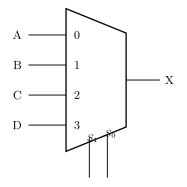
Figure 11: Question 22’s 4-to-1 multiplexer, with its four data inputs A, B, C, D and the select pair \(S_1 S_0\).
A=0, B=1, C=0, D=0
A=0, B=1, C=1, D=1
A=1, B=0, C=1, D=1
A=1, B=1, C=0, D=1
None of the above
TipAnswer
(c)
The select pair \(S_1 S_0\) read as a two-bit number picks the data input of that number, so A is chosen for \(S_1S_0 = 00\), B for \(01\), C for \(10\) and D for \(11\). Each data input therefore just has to be the value the function takes for that one select combination — with no variables left over, the inputs are all constants:
| \(S_1\) | \(S_0\) | input chosen | \(X = \overline{S_0} + S_1\) |
|---|---|---|---|
| 0 | 0 | A | \(1 + 0 = 1\) |
| 0 | 1 | B | \(0 + 0 = 0\) |
| 1 | 0 | C | \(1 + 1 = 1\) |
| 1 | 1 | D | \(0 + 1 = 1\) |
So A = 1, B = 0, C = 1, D = 1, which is option (c). Reading the data inputs top to bottom gives the function’s truth-table column directly — that is the whole trick to using a multiplexer as a function generator, see combinational-logic-blocks.
Q23 — Which circuit is a latch
Which of the following circuits is capable of acting as a latch? i.e. it has combinations of inputs (M,N) which allow a bit (0 or 1) to be stored, the latch to be set (Q=1) with a single input transition, and the latch to be cleared (Q=0) with a single input transition?
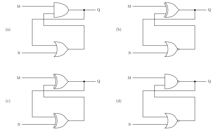
Figure 12: Question 23’s four candidate cross-coupled circuits. In each one Q is the top gate’s output, and it is fed back to the bottom gate whose output returns to the top gate.
- None of the above
TipAnswer
(a)
Each circuit is the same feedback loop with different gates, so write the loop equation and look for a hold state.
(a) — AND on top, OR underneath: \(Q = M . (Q + N)\).
| M | N | \(Q = M.(Q+N)\) | behaviour |
|---|---|---|---|
| 0 | 0 | \(0\) | clear |
| 0 | 1 | \(0\) | clear |
| 1 | 0 | \(Q\) | hold |
| 1 | 1 | \(1\) | set |
Sitting in the hold state \((M,N) = (1,0)\), taking N to 1 sets it and taking M to 0 clears it — one input transition each, and both return to holding when the input goes back. This is the classic AND–OR latch (N is set, M is an active-low reset), so (a) is the answer.
(b) — XOR on top, NOR underneath: \(Q = M \oplus \overline{Q + N}\). At \((1,0)\) this is \(1 \oplus \overline{Q} = Q\), so it holds; at \((1,1)\) it forces \(Q = 1\); but the only clearing combination is \((0,1)\), which is two transitions away from the hold state, and \((0,0)\) gives \(Q = \overline{Q}\), which oscillates rather than settling.
(c) — XOR on top and bottom: \(Q = M \oplus Q \oplus N\). That is stable only when \(M \oplus N = 0\), and then \(Q = Q\) for both \((0,0)\) and \((1,1)\) — it can hold but can never be forced to a value, so it can be neither set nor cleared. When \(M \neq N\) it oscillates.
(d) — NAND on top, NOR underneath: \(Q = \overline{M . \overline{Q + N}}\). With \(M = 0\) the output is forced to 1; with \(M = 1\) it reduces to \(Q + N\), which holds at \(N = 0\) and sets at \(N = 1\). There is no combination that forces \(Q = 0\), so it can never be cleared.
See flip-flops-and-latches for the standard NOR and NAND cross-coupled latches this question is testing against.
Q24 — ALU control settings
Consider the ALU bit slice below.
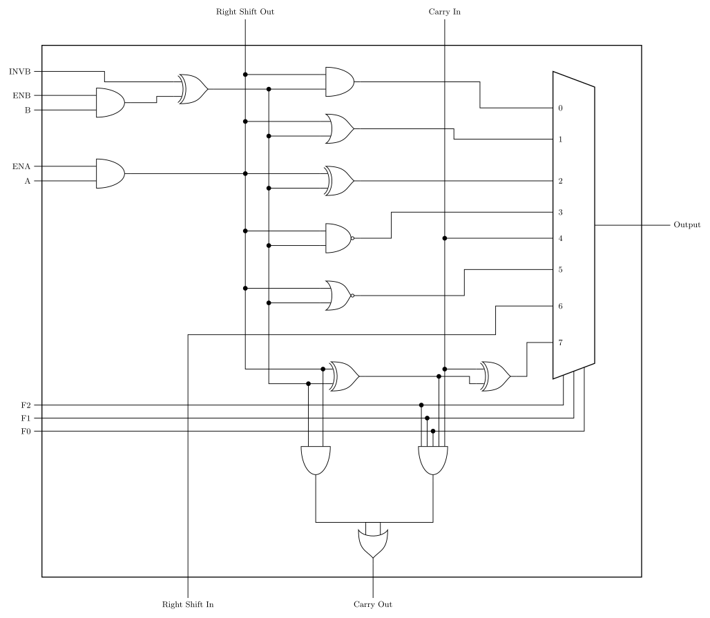
Figure 13: Question 24’s ALU bit slice. The ENA/ENB/INVB gates on the left condition A and B into internal lines X and Y; five logic gates and the full adder compute candidate results from them, and the 8-way multiplexer picks one under \(F_2 F_1 F_0\). Note that the conditioned A line is also what leaves as Right Shift Out.
For an ALU made up of 8 of the bit slices above, which of the following control input settings will result in the ALU output being \(\overline{A} . B\) ? (The “Right Shift In” control input refers to that for the most significant bit; the “Carry in” control input refers to that for the least significant bit.)
ENA = 1, ENB = 1, INVB = 0, \(F_2\) = 0, \(F_1\) = 0, \(F_0\) = 0, Right Shift In = 0, Carry in = 0
ENA = 1, ENB = 1, INVB = 1, \(F_2\) = 0, \(F_1\) = 1, \(F_0\) = 1, Right Shift In = 0, Carry in = 1
ENA = 1, ENB = 1, INVB = 0, \(F_2\) = 0, \(F_1\) = 1, \(F_0\) = 1, Right Shift In = 0, Carry in = 1
ENA = 1, ENB = 1, INVB = 1, \(F_2\) = 1, \(F_1\) = 0, \(F_0\) = 1, Right Shift In = 0, Carry in = 0
ENA = 1, ENB = 1, INVB = 1, \(F_2\) = 1, \(F_1\) = 1, \(F_0\) = 1, Right Shift In = 0, Carry in = 1
TipAnswer
(d)
Start from the conditioning gates. Writing \(X\) for the conditioned A line and \(Y\) for the conditioned B line,
\[X = A . \text{ENA} \qquad Y = (B . \text{ENB}) \oplus \text{INVB}\]
so with ENA = ENB = 1, \(X = A\) and \(Y\) is \(B\) when INVB = 0 or \(\overline{B}\) when INVB = 1. Note there is no INVA on this slice, so \(\overline{A}\) is never available directly — that is the crux of the question.
Tracing each multiplexer input back to the gate that drives it gives the function table:
| \(F_2 F_1 F_0\) | multiplexer input | Output |
|---|---|---|
| 000 | 0 | \(X . Y\) |
| 001 | 1 | \(X + Y\) |
| 010 | 2 | \(X \oplus Y\) |
| 011 | 3 | \(\overline{X . Y}\) |
| 100 | 4 | Carry In |
| 101 | 5 | \(\overline{X + Y}\) |
| 110 | 6 | Right Shift In |
| 111 | 7 | \(X \oplus Y \oplus C_{in}\) (the adder sum) |
Since \(\overline{A}\) cannot be produced by the input conditioning, the inversion has to come from a gate. De Morgan supplies it:
\[\overline{A} . B = \overline{A + \overline{B}}\]
which is the NOR of \(A\) and \(\overline{B}\) — i.e. set INVB = 1 so \(Y = \overline{B}\), and select the NOR at input 5, \(F_2F_1F_0 = 101\). That is option (d), and its Right Shift In and Carry in are irrelevant to a purely logical operation.
Checking the others: (a) selects the AND with \(Y = B\), giving \(A . B\); (b) and (c) both select the NAND (\(F_2F_1F_0 = 011\)) and differ only in INVB, giving \(\overline{A . \overline{B}} = \overline{A} + B\) and \(\overline{A . B}\) respectively; (e) selects the adder with \(Y = \overline{B}\) and carry in 1, giving \(A \oplus \overline{B} \oplus 1 = A \oplus B\). See arithmetic-logic-unit.
Q25 — ALU operation coverage
For the ALU in question 24, which of the following bitwise logical operations can NOT be performed?
\(\overline{A} + B\)
\(A \oplus \overline{B}\)
\(\overline{A} \oplus B\)
\(\overline{A . B}\)
All of the above operations can be performed
TipAnswer
(e)
Using the same reading of the slice as Q24: \(X\) can be \(A\) or \(0\), \(Y\) can be \(B\), \(\overline{B}\), \(0\) or \(1\), and the five logic functions available are AND, OR, XOR, NAND and NOR of \(X\) and \(Y\). Setting ENA = ENB = 1 and choosing INVB and \(F_2F_1F_0\):
| Wanted | Rewrite | Settings |
|---|---|---|
| (a) \(\overline{A} + B\) | \(\overline{A . \overline{B}}\) | INVB = 1, NAND (\(F = 011\)) |
| (b) \(A \oplus \overline{B}\) | as written | INVB = 1, XOR (\(F = 010\)) |
| (c) \(\overline{A} \oplus B\) | \(= A \oplus \overline{B}\) | INVB = 1, XOR (\(F = 010\)) |
| (d) \(\overline{A . B}\) | as written | INVB = 0, NAND (\(F = 011\)) |
All four are reachable, so the answer is (e).
The one worth pausing on is (c). Complementing either operand of an XOR complements the result, so \(\overline{A} \oplus B\) and \(A \oplus \overline{B}\) are the same function — both are \(\overline{A \oplus B}\), i.e. XNOR — and the slice can produce it even though it has no INVA. The absence of INVA restricts less than it looks like it should: De Morgan and the XOR identity between them let the missing complement be pushed onto B.
Beyond the paper — the adder as a real chip
Q13, Q14 and Q15 all run the same adder by hand, and Q16 builds one out of multiplexers. Learning Lab 3 (Binary Arithmetic) builds it out of a single part instead, and the schematic is worth having in front of you, because three of this paper’s traps are visible in it as separate wires.
This is Task 2 of Learning Lab 3 (Binary Arithmetic), drawn to the rules in circuit-schematics with the symbol and pin numbers from the Device Pinouts and Symbols sheet. The particular signal-to-pin assignments on the IO board are a free choice. The sheet fixes the ranges (switches on pins 25–32, buttons on 12–15, LEDs on 17–24) but not which switch carries which bit. See week2-lab-binary-arithmetic for the rest of the lab.
The task
Add two 4-bit numbers set on switches, show the 4-bit result and the carry out on LEDs, and put the carry in on a push button. One chip does all the arithmetic: the 74HCT283, four full adders in a 16-pin package with the intermediate carries \(C_1\), \(C_2\), \(C_3\) joined stage to stage inside it, so only \(C_0\) and \(C_4\) appear on pins.
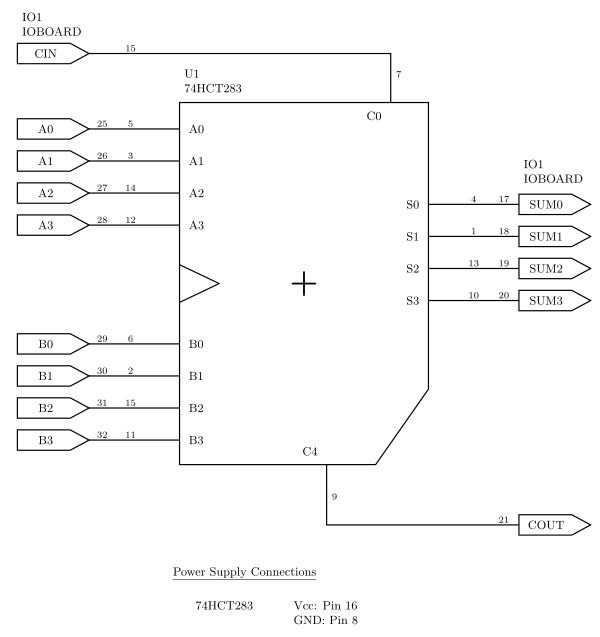
Figure 14: Lab 3 Task 2 as a circuit schematic: a 74HCT283 adding two 4-bit numbers from IO-board switches, with the carry in on a push button and the sum and carry out on LEDs. Everything a schematic is required to carry is here — a unique name on every input and output, the device identifier U1 with its type underneath, a pin number at both ends of every wire, the IO board labelled once per group rather than once per signal, and a power block giving Vcc and GND for the device type. The 74HCT283 is a 16-pin part, so its supply pins are 16 and 8 — not the 14 and 7 of the quad gate packages, which is the mistake this schematic exists to prevent. The input pentagons attach their wire at the point and the output pentagons at the flat back; getting that round the wrong way is one of the errors the drawing guide lists.
One adder, two interpretations
The lab’s instruction after building it is “try some unsigned and two’s complement test cases — are the results as you expect?”, and the answer is the point of the whole exercise: the chip does not know which you meant. It adds bit patterns. Nothing inside it changes between Q13’s two’s complement reading and an unsigned one; the same eight switches and the same five LEDs serve both. What changes is only which condition means the answer on the LEDs is wrong:
| Reading | Range in 4 bits | The answer is wrong when |
|---|---|---|
| Unsigned | 0 to 15 | \(C_4 = 1\) — the true sum needed a fifth bit |
| Two’s complement | \(-8\) to \(+7\) | the operands’ sign bits agreed and \(S_3\) disagrees with them |
That is why \(C_4\) gets its own LED separate from the sum. It is also precisely the trap in Q15: \(1010 + 0110\) produces \(C_4 = 1\), and the answer is still exactly right, because the reading is two’s complement and the carry out is discarded rather than consulted.
The extension, and what it needs
The lab then asks for an overflow LED as well, with a constraint that changes the problem: “you don’t have access to C3 which is an internal signal. Therefore, you need the overflow output expressed in terms of available information (i.e. A3, B3, S3, C4).” Reading the schematic explains why — \(C_3\) is joined to the next full adder inside the package and never reaches a pin, so the familiar \(V = C_3 \oplus C_4\) cannot be wired.
The two expressions that can be wired from pins are
\[V = A_3 B_3 \overline{S_3} + \overline{A_3}\,\overline{B_3}\,S_3 \qquad\text{and}\qquad V = A_3 \oplus B_3 \oplus S_3 \oplus C_4\]
both of which are derived and drawn in csse2010-sample-midsem-2. The second is the cheaper build — three XOR gates, one 74HCT86 — and it is the reason \(C_4\) is among the signals you are allowed to use. Either one, driven onto an LED, turns Q14 from a decimal calculation into something the board tells you.
Where Q16 fits
Q16’s pair of multiplexers implements one of the four full adders inside this package. Cascading four of them, carry to carry, is what the 74HCT283 has done for you — see combinational-logic-blocks for the ripple-carry structure and device-pinouts for the chip’s internals as the source sheet draws them.
Your score
Reload the page to clear your answers.