Binary Arithmetic Lab
Learning Lab 3 — binary arithmetic revision, then circuits that do arithmetic, simulated in Logisim and built with ICs. Pairs with 2026-08-04-binary-arithmetic.
Worked: \(-16_{10}\) in 8-bit two’s complement
11110000.
\(16 = \texttt{00010000}\); invert to 11101111; add 1 to get 11110000. Check: \(-128 + 64 + 32 + 16 = -16\). ✓
The wrong answers to watch for: 11101111 is the ones’ complement — the answer if you forget the \(+1\). 10010000 and 10010001 are the signed-magnitude and signed-magnitude-off-by-one answers, and 00010000 is \(+16\), i.e. the magnitude with the negation left out altogether.
Worked: 001110 + 110100 in 6-bit two’s complement
000010, with no overflow.
\(001110_2 = 14\) and \(110100_2 = -32 + 16 + 4 = -12\), so the true answer is \(2 = \texttt{000010}\). ✓
Overflow check, with the carry row written out:
| \(c_5\) | \(c_4\) | \(c_3\) | \(c_2\) | \(c_1\) | \(c_0\) | ||
|---|---|---|---|---|---|---|---|
| carry in | 1 | 1 | 1 | 0 | 0 | 0 | ← carry into each column |
| 0 | 0 | 1 | 1 | 1 | 0 | \(= 14\) | |
| 1 | 1 | 0 | 1 | 0 | 0 | \(= -12\) | |
| sum | 0 | 0 | 0 | 0 | 1 | 0 | \(= 2\) |
The carry into the MSB is 1 and the carry out is also 1, so \(C_{in} \oplus C_{out} = 0\) — no overflow. The carry-out of 1 would signal overflow if these were unsigned. Getting the sum right is not enough: the answer has to say whether it overflows as well; see 2026-08-04-binary-arithmetic.
Worked: which operation overflows in 4-bit two’s complement?
4-bit two’s complement covers \(-8\) to \(7\).
| Operation | Result | Overflow? | |
|---|---|---|---|
| A | 0100 − 0101 |
\(4 - 5 = -1\) | no |
| B | 1001 − 0001 |
\(-7 - 1 = -8\) | no (just fits) |
| C | 0100 + 0101 |
\(4 + 5 = 9\) | yes — 9 > 7 |
| D | 1001 + 0001 |
\(-7 + 1 = -6\) | no |
Answer: C. B is the near-miss: \(-8\) is exactly representable, so it does not overflow.
Task 1 — 1-bit full adder
Turn the full-adder logic diagram (two XORs, two ANDs and an OR) into a circuit schematic, using switches for the three inputs (\(A\), \(B\), carry-in) and LEDs for the two outputs (sum, carry-out). Have it checked by a tutor, then simulate, build and test it — systematically, against the full-adder truth table. The gate-level diagram itself is in 2026-08-04-binary-arithmetic; the equations it implements are
\[S = A \oplus B \oplus C_{in} \qquad C_{out} = AB + C_{in}(A \oplus B)\]
The two-chip challenge
The challenge: build the full adder using only two chips.
The literal reading of the diagram needs three chips — a 74HCT86 for the two XORs, a 74HCT08 for the two ANDs and a 74HCT32 for the OR. Going all-NAND does not help: a full adder in NAND alone takes nine 2-input NAND gates, and a 74HCT00 holds four, so that route needs three chips too.
The two-chip answer is to convert only the carry expression to NAND and leave the sum as XORs. De Morgan on \(C_{out}\):
\[C_{out} = AB + C_{in}(A\oplus B) = \overline{\overline{AB}\cdot\overline{C_{in}(A\oplus B)}} = \text{NAND}\big(\text{NAND}(A,B),\ \text{NAND}(C_{in}, A\oplus B)\big)\]
That is two XOR gates and three NAND gates — two of the four gates on a 74HCT86 and three of the four on a 74HCT00. Two chips, with one spare gate in each.
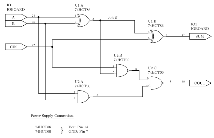
Figure 1: The Task 1 circuit schematic in its two-chip form: a 74HCT86 supplies the two XOR gates of the sum path and a 74HCT00 the three NAND gates of the carry path. Drawn to the rules in circuit-schematics — device ID and type on every gate, a pin number on every terminal, IO board inputs attached at the point of the pentagon and outputs at its flat back, and one power block because both chips are 14-pin parts with Vcc on 14 and GND on 7. The four junction dots — one at each fan-out of A, B, CIN and A-xor-B — are the only connections; where CIN’s branch to U1:B crosses the A-xor-B drop, and where the switch wires cross CIN’s run, the wires pass without a dot.
The stages of completion, in order: schematic done / simulated / partially working / fully working with 3 ICs / fully working with 2 ICs. The two-chip build is the top rung, not an optional extra. (Completion is self-reported, not marked.)
See combinational-logic-blocks for the adder structure and circuit-schematics for the drawing rules.
Task 2 — 4-bit adder with the 74HCT283
The 74HCT283 is a single-chip 4-bit adder. Draw a schematic that adds two 4-bit numbers set on switches, showing the 4-bit result and the carry-out on LEDs, with the carry-in on a push button.
- Use the Device Pinouts and Symbols symbol: a trapezoid with \(A_0\)–\(A_3\) on the upper left (pins 5, 3, 14, 12), \(B_0\)–\(B_3\) on the lower left (pins 6, 2, 15, 11), \(C_0\) entering the top (pin 7), \(S_0\)–\(S_3\) on the right (pins 4, 1, 13, 10) and \(C_4\) leaving the bottom (pin 9). See device-pinouts.
- Don’t forget the power connections. It’s a 16-pin chip: Vcc is pin 16 and GND pin 8, not 14/7 as on every gate chip you have used so far.
- Have the schematic checked, then wire it up, test it and simulate it. Try both unsigned and two’s complement test cases and check the results are what you expect. (They are the same four bits either way; only your reading of them changes, and only \(C_4\) versus the overflow rule tells you whether that reading is valid.)
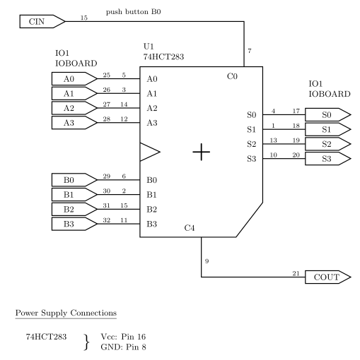
Figure 2: The Task 2 schematic. Eight switches supply the two operands, a push button supplies the carry-in, and five LEDs show the sum and the carry-out. The one thing this figure exists to make unmissable is the power block: the 74HCT283 is a 16-pin package, so its supply pins are 16 and 8, and a schematic that reuses 14/7 out of habit is wrong. The switch, button and LED pin assignments are chosen from the IO board pin list in device-pinouts.
Extension — overflow detector
Add a two’s-complement overflow detector driving an LED. The catch:
There is no access to \(C_3\), which is an internal signal. The overflow output has to be expressed in terms of available information — i.e. \(A_3\), \(B_3\), \(S_3\), \(C_4\).
The usual formula \(V = C_3 \oplus C_4\) is therefore unavailable: the 74HCT283 chains \(C_1\), \(C_2\) and \(C_3\) inside the package and only brings out \(C_0\) and \(C_4\).
The rule that uses only the pins you can reach is: overflow happens exactly when both operands share a sign and the result’s sign differs from it. Adding two negatives can’t give a positive; adding two positives can’t give a negative. As an expression,
\[V = A_3 B_3 \overline{S_3} + \overline{A_3}\,\overline{B_3} S_3\]
\(C_4\) is available but not needed — the sign bits alone settle it.
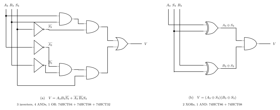
Figure 3: Two ways to build the overflow LED, both using only the pins the 74HCT283 brings out. (a) is the sum-of-products form read straight off the rule, and costs three chips because the kit has no gate with more than two inputs, so each three-literal product needs two ANDs. (b) is the same function factored as a product of two XORs: A3 differs from S3 and B3 differs from S3 exactly when the two operands agree in sign and the sum does not. Its two XORs are exactly the pair left spare on Task 1’s 74HCT86, though the AND still needs a chip of its own: Task 1’s 74HCT00 has only one gate free, and an AND built from NANDs takes two.
The stages of completion for Task 2: schematic done / partially working / fully working 4-bit adder / fully working with overflow detection. Again, the extension is the top rung.
Next
Lab 4 has a preparation task to be done before the session — see week3-lab-lab-4-pre-work.