Sample Mid-semester Exam #2
exercises
exam
past-paper
computer-systems
The second of UQ’s sample mid-semester papers for CSSE2010/CSSE7201 Introduction to Computer Systems — see csse2010 for the course note. The cover page is from the Semester One mid-semester examinations, 2020, for St Lucia campus students. It allows 60 minutes of working time plus 10 minutes of reading time, is an open book examination with no electronic aids other than a Casio FX82-series or UQ-approved calculator, and is answered on a supplied multiple choice answer sheet. There are 25 questions, each worth one mark, and the marking is “choose the answer which best answers the question or completes the statement” — a correct answer scores one mark, and an incorrect, missing or multiple answer scores zero. There is no penalty for guessing.
WarningAnswers are derived, not official
The source paper ships without an answer key, so every answer below was worked out during transcription rather than taken from UQ. Each one shows its reasoning so it can be checked rather than trusted; anything uncertain is flagged. Treat a disagreement between your working and the answer here as a reason to check both.
How to use this
Two ways. Timed run — sit all 25 questions in 60 minutes as if it were the real thing; on the website the answers are collapsed, so they stay hidden until you click them. Targeted practice — use the index table below to pick out only the questions for one week or one concept, and follow the wikilink to the note that covers the method.
Note that the PDF build of this vault renders every callout expanded, so the answers are visible there. Practise from the site version.
Question index
| Q | Topic | Week | Concept notes |
|---|---|---|---|
| 1 | Two’s complement representation | 1 | binary-number-representations |
| 2 | Octal, hex and decimal | 1 | binary-number-representations |
| 3 | Excess-N range | 1 | binary-number-representations |
| 4 | One’s complement to excess-N | 1 | binary-number-representations |
| 5 | Reading a gate circuit | 1 | logic-gates · boolean-algebra |
| 6 | Circuit for an XOR function | 1 | logic-gates |
| 7 | Boolean simplification | 1 | boolean-algebra |
| 8 | Truth table for an XOR chain | 1 | logic-gates |
| 9 | Sum of products from a table | 1 | boolean-algebra |
| 10 | XOR identities | 1 | boolean-algebra · logic-gates |
| 11 | NAND as a universal gate | 1 | logic-gates |
| 12 | Multiplexer as function generator | 2 | combinational-logic-blocks |
| 13 | Two’s complement addition | 2 | binary-number-representations |
| 14 | D flip-flop timing | 3 | flip-flops-and-latches · timing-diagrams |
| 15 | NOR SR latch behaviour | 3 | flip-flops-and-latches |
| 16 | Shift register with function select | 3 | shift-registers |
| 17 | Synchronous counter sequence | 4 | counters · sequential-circuits |
| 18 | Overflow detection | 2 | binary-number-representations |
| 19 | Overflow in a signed addition | 2 | binary-number-representations |
| 20 | State table to state diagram | 4 | state-machines |
| 21 | Flip-flops needed for a machine | 4 | state-machines |
| 22 | Tracing a state machine | 4 | state-machines |
| 23 | ALU control for NOR | 5 | arithmetic-logic-unit |
| 24 | ALU control for NOT B | 5 | arithmetic-logic-unit |
| 25 | Half adder from multiplexers | 2 | combinational-logic-blocks |
Q1 — Two’s complement representation
What is \(-27_{10}\) expressed in 7-bit two’s complement format?
0011011
1011011
1100100
1100101
1100110
TipAnswer
(d)
Two’s complement negation is “invert every bit, then add one”. Start from \(+27\) in seven bits:
\[27 = 16 + 8 + 2 + 1 = 0011011_2\]
Invert: \(1100100\). Add one: \(1100100 + 1 = 1100101\).
The distractors are the intermediate steps, which is exactly the trap: (a) is \(+27\), (c) is the one’s complement (the inverted bits, before the \(+1\)), and (b) is \(+27\) with only the sign bit flipped, i.e. sign-and-magnitude. See binary-number-representations.
Q2 — Octal, hex and decimal
\(110_8\) is equal to
\(10001000_2\)
\(68_{10}\)
0x48
\(6_{10}\)
None of the above
TipAnswer
(c)
Octal digits are worth powers of 8, so
\[110_8 = 1 \times 8^2 + 1 \times 8^1 + 0 \times 8^0 = 64 + 8 = 72_{10}\]
Checking each option: (a) \(10001000_2 = 128 + 8 = 136\); (b) 68; (c) \(0\text{x}48 = 4 \times 16 + 8 = 72\) ✓; (d) 6.
The quick route avoids decimal altogether — each octal digit is three bits, so \(110_8 = 001\,001\,000_2 = 0100\,1000_2\), and regrouping those bits into nibbles reads straight off as 0x48. See binary-number-representations.
Q3 — Excess-N range
A 10-bit binary number in excess-512 representation can represent integers from
-512 to 511
-512 to 512
-511 to 511
-511 to 512
None of the above
TipAnswer
(a)
In excess-\(N\), the stored bit pattern is the value plus the bias: \(\text{pattern} = \text{value} + N\). Ten bits hold the unsigned patterns \(0\) through \(1023\), so with \(N = 512\):
\[\text{value} = \text{pattern} - 512 \quad\Rightarrow\quad 0 - 512 = -512 \;\text{ to }\; 1023 - 512 = 511\]
That is the same range as 10-bit two’s complement, which is the point of choosing the bias to be \(2^{n-1}\) — the two representations differ only in the most significant bit. See binary-number-representations.
Q4 — One’s complement to excess-N
How can any n-bit binary number in one’s complement representation be converted to excess-2n-1 representation?
By flipping the most-significant bit and then adding 1
By flipping the most-significant bit and then adding the value of the most-significant bit
By adding the value of the most-significant bit and then flipping the most-significant bit
By adding the value of the most-significant bit and flipping all the bits
By flipping all the bits except the most-significant bit
TipAnswer
(c)
Go through two’s complement, because each leg is a one-line rule:
- One’s complement → two’s complement. The two representations agree on non-negative values; for negative values the one’s complement pattern is one less than the two’s complement one. So add 1 when the number is negative and 0 when it is not — and “is it negative” is exactly the most significant bit. Adding the value of the MSB does both cases at once.
- Two’s complement → excess-\(2^{n-1}\). Adding the bias \(2^{n-1}\) modulo \(2^n\) is the same thing as flipping the most significant bit, because \(2^{n-1}\) is the MSB’s weight.
Doing those in order gives (c). Worked on \(n = 4\), with the pattern \(1000\) (one’s complement \(-7\)): add the MSB, \(1000 + 1 = 1001\) (two’s complement \(-7\)); flip the MSB, \(0001 = 1\), and \(-7 + 8 = 1\) ✓.
Option (b) has the same two steps in the other order, and this is where the word any in the question earns its underline. Read literally, (b) flips the MSB first, so “the value of the most-significant bit” it then adds is the flipped bit — the opposite of what is wanted. Only (c) reads the MSB while it still means “is this number negative”.
Check this one. If you read the “value of the most-significant bit” in (b) as the value it had before the flip, then (b) and (c) describe the same operation and both are correct — flipping the MSB is addition of \(2^{n-1}\) modulo \(2^n\), which commutes with adding 1. The paper can only have one answer, so the intended distinction must be the reading above, but it rests on wording rather than on arithmetic.
Q5 — Reading a gate circuit
What function is implemented by the following circuit?
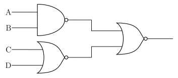
Figure 1: Question 5’s circuit: a NAND on A and B, a NOR on C and D, and a NOR combining the two.
\((\overline{A.B}) + (\overline{C + D})\)
\(\overline{(\overline{A.B}) + (\overline{C + D})}\)
\(\overline{(\bar{A}.\bar{B}) + (\overline{C + D})}\)
\((\overline{A.B}) \oplus (\overline{C + D})\)
\((\overline{A.B}) \oplus (C \oplus D)\)
TipAnswer
(b)
Name the two first-stage outputs and then wrap them in the output gate. The top gate is an AND with a bubble, so it is a NAND: \(P = \overline{A \cdot B}\). The bottom gate is an OR with a bubble, so it is a NOR: \(Q = \overline{C + D}\). The output gate is an OR with a bubble, so it is a NOR of those two:
\[X = \overline{P + Q} = \overline{(\overline{A.B}) + (\overline{C+D})}\]
which is (b) verbatim. Option (a) is the same expression without the final inversion — the trap for anyone who reads the last gate as a plain OR.
Simplifying confirms it is not any of the others: De Morgan turns \(X = \overline{P + Q}\) into \(\overline{P} \cdot \overline{Q}\), and \(\overline{P}\) and \(\overline{Q}\) undo the two first-stage bubbles, so \(X = (A \cdot B) \cdot (C + D)\). The circuit is really “A and B, and at least one of C or D”. See logic-gates for the bubble-means-invert convention and boolean-algebra for De Morgan.
Q6 — Circuit for an XOR function
Which of the following circuits implements the function \(A \oplus (B + C) \oplus D\)
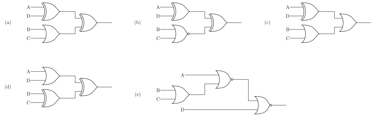
Figure 2: Question 6’s five candidate circuits, laid out (a) to (e) as they appear on the paper.
TipAnswer
(a)
XOR is both commutative and associative, so the target function can be regrouped freely:
\[A \oplus (B + C) \oplus D = (A \oplus D) \oplus (B + C)\]
That is exactly circuit (a): an XOR on A and D, an OR on B and C, and an XOR joining them.
The others each break one gate. (b) replaces the OR with a NOR, giving \((A \oplus D) \oplus \overline{B + C}\) — the complement of the right answer, since inverting one input of an XOR inverts its output. (c) uses an OR as the final gate rather than an XOR. (d) swaps the two first-stage gates, giving \((A + D) \oplus (B \oplus C)\). (e) is built from NORs and computes \(\overline{\overline{A + (B+C)} + D}\), which is not an XOR of anything. See logic-gates.
Q7 — Boolean simplification
Which of the following logic functions is equivalent to \(\overline{(A + B.\bar{C}).(\overline{\bar{A} + B})}\)
\(\bar{A} + B\)
\(\bar{A} + C + B\)
\(A.\bar{B}\)
\(\bar{A}.C + B\)
None of the above
TipAnswer
(a)
Write \(P = A + B\bar{C}\) and \(Q = \bar{A} + B\), so the expression is \(\overline{P \cdot \bar{Q}}\). De Morgan turns that into a sum:
\[\overline{P \cdot \bar{Q}} = \bar{P} + \bar{\bar{Q}} = \bar{P} + Q\]
Now expand \(\bar{P}\) with De Morgan again:
\[\bar{P} = \overline{A + B\bar{C}} = \bar{A} \cdot \overline{B\bar{C}} = \bar{A}(\bar{B} + C)\]
so
\[\bar{P} + Q = \bar{A}\bar{B} + \bar{A}C + \bar{A} + B\]
Every one of the first two terms contains \(\bar{A}\), so absorption collapses them into the standalone \(\bar{A}\):
\[\bar{A}\bar{B} + \bar{A}C + \bar{A} = \bar{A}\]
leaving \(\bar{A} + B\), which is (a).
Sanity check without any algebra: the whole expression is \(\bar{P} + Q\), and \(Q = \bar{A} + B\) is false only when \(A = 1, B = 0\). In that case \(P = 1 + 0 = 1\), so \(\bar{P} = 0\) and the expression is 0 too. Whenever \(Q\) is true the expression is true. So the expression equals \(Q = \bar{A} + B\) exactly. See boolean-algebra.
Q8 — Truth table for an XOR chain
What is the truth table corresponding to \(= \bar{A} \oplus \bar{B} \oplus \bar{C}\) ?
| A | B | C | X | |
|---|---|---|---|---|
| (a) | 0 | 0 | 0 | 0 |
| 0 | 0 | 1 | 1 | |
| 0 | 1 | 0 | 1 | |
| 0 | 1 | 1 | 0 | |
| 1 | 0 | 0 | 1 | |
| 1 | 0 | 1 | 0 | |
| 1 | 1 | 0 | 0 | |
| 1 | 1 | 1 | 1 | |
| (b) | 0 | 0 | 0 | 0 |
| 0 | 0 | 1 | 1 | |
| 0 | 1 | 0 | 1 | |
| 0 | 1 | 1 | 0 | |
| 1 | 0 | 0 | 1 | |
| 1 | 0 | 1 | 0 | |
| 1 | 1 | 0 | 0 | |
| 1 | 1 | 1 | 0 | |
| (c) | 0 | 0 | 0 | 0 |
| 0 | 0 | 1 | 0 | |
| 0 | 1 | 0 | 0 | |
| 0 | 1 | 1 | 1 | |
| 1 | 0 | 0 | 0 | |
| 1 | 0 | 1 | 1 | |
| 1 | 1 | 0 | 1 | |
| 1 | 1 | 1 | 0 | |
| (d) | 0 | 0 | 0 | 1 |
| 0 | 0 | 1 | 0 | |
| 0 | 1 | 0 | 0 | |
| 0 | 1 | 1 | 0 | |
| 1 | 0 | 0 | 0 | |
| 1 | 0 | 1 | 0 | |
| 1 | 1 | 0 | 0 | |
| 1 | 1 | 1 | 1 | |
| (e) | 0 | 0 | 0 | 1 |
| 0 | 0 | 1 | 0 | |
| 0 | 1 | 0 | 0 | |
| 0 | 1 | 1 | 1 | |
| 1 | 0 | 0 | 0 | |
| 1 | 0 | 1 | 1 | |
| 1 | 1 | 0 | 1 | |
| 1 | 1 | 1 | 0 |
TipAnswer
(e)
XOR has a useful property: inverting two of its inputs leaves the result unchanged, because the two inversions cancel. Inverting an odd number of inputs inverts the output. Here all three inputs are inverted, so
\[\bar{A} \oplus \bar{B} \oplus \bar{C} = \overline{A \oplus B \oplus C}\]
and \(A \oplus B \oplus C\) is the odd-parity function — 1 when an odd number of the inputs is 1. Its complement is even parity, so \(X = 1\) exactly when the row contains an even number of 1s:
| A B C | number of 1s | X |
|---|---|---|
| 0 0 0 | 0 | 1 |
| 0 0 1 | 1 | 0 |
| 0 1 0 | 1 | 0 |
| 0 1 1 | 2 | 1 |
| 1 0 0 | 1 | 0 |
| 1 0 1 | 2 | 1 |
| 1 1 0 | 2 | 1 |
| 1 1 1 | 3 | 0 |
That column is 1 0 0 1 0 1 1 0, which is option (e). Option (a) is the exact complement of it — odd parity, i.e. the answer you get if you forget that three inversions do not cancel.
The paper writes the question as “corresponding to \(= \bar{A} \oplus \bar{B} \oplus \bar{C}\)”, with a stray equals sign; the function is clearly meant to be \(X = \bar{A} \oplus \bar{B} \oplus \bar{C}\). See logic-gates.
Q9 — Sum of products from a table
Consider the logic function represented by the following truth table:
| A | B | C | X |
|---|---|---|---|
| 0 | 0 | 0 | 0 |
| 0 | 0 | 1 | 1 |
| 0 | 1 | 0 | 1 |
| 0 | 1 | 1 | 1 |
| 1 | 0 | 0 | 0 |
| 1 | 0 | 1 | 1 |
| 1 | 1 | 0 | 0 |
| 1 | 1 | 1 | 1 |
Which of the following expressions is equivalent to the function represented by this table?
\(\bar{A}.B + A.C\)
\(A.C + (B + C)\)
\(\bar{A}.B + C\)
\(\bar{A}.B + B.C + \bar{A}.C\)
None of the above
TipAnswer
(c)
Read off the rows where \(X = 1\): 001, 010, 011, 101, 111. As a sum of products,
\[X = \bar{A}\bar{B}C + \bar{A}B\bar{C} + \bar{A}BC + A\bar{B}C + ABC\]
Four of those five minterms — 001, 011, 101, 111 — are every row with \(C = 1\), and together they simplify to just \(C\). That leaves 010, i.e. \(\bar{A}B\bar{C}\):
\[X = C + \bar{A}B\bar{C}\]
and \(C + \bar{A}B\bar{C} = C + \bar{A}B\) by absorption (adding \(\bar{A}B\) where \(C\) is already 1 changes nothing). So \(X = \bar{A}.B + C\), which is (c).
Checking (c) against all eight rows: it is 1 whenever \(C = 1\) (four rows) and, among the \(C = 0\) rows, only for \(A=0, B=1\) — exactly the five rows above. See boolean-algebra.
Q10 — XOR identities
Which of the following logic functions is identical to \(\bar{A} \oplus \bar{B}\)?
\(A.\bar{B} + \bar{A}.B\)
\(\bar{A}.\bar{B} + \bar{B}.\bar{A}\)
\(\bar{A} + \bar{B}\)
\(\overline{A \oplus B}\)
None of the above
TipAnswer
(a)
Inverting both inputs of a two-input XOR leaves it unchanged — the two inversions cancel, as in Q8:
\[\bar{A} \oplus \bar{B} = A \oplus B\]
and the definition of XOR is \(A \oplus B = A\bar{B} + \bar{A}B\), which is (a) as written.
The others: (b) is \(\bar{A}\bar{B} + \bar{A}\bar{B} = \bar{A}\bar{B}\), i.e. NOR, since the two product terms are the same term written in the opposite order. (c) is NAND, by De Morgan. (d) is XNOR — the complement of the right answer, and the trap for treating the two bars as if they inverted the result once rather than twice. See boolean-algebra.
Q11 — NAND as a universal gate
Which of the following implements a 3-input NAND gate \((\overline{A.B.C})\) using only 2-input NAND gates?
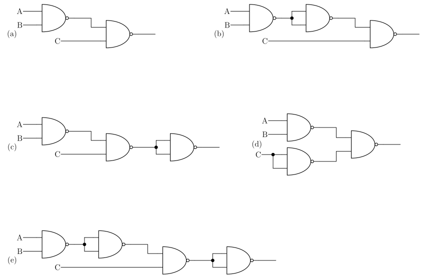
Figure 3: Question 11’s five candidate NAND-only circuits. Where a NAND’s two inputs are tied together it is acting as an inverter.
TipAnswer
(b)
A NAND with both inputs tied together is an inverter, since \(\overline{X \cdot X} = \bar{X}\). That is the only extra building block needed, because the target \(\overline{ABC}\) is “AND the three, then invert”, and a NAND followed by an inverter is an AND.
Working through (b): the first NAND gives \(\overline{AB}\); the second has its inputs tied, so it inverts that back to \(AB\); the third NANDs \(AB\) with \(C\):
\[\overline{(A \cdot B) \cdot C} = \overline{A.B.C} \;✓\]
The others:
- (a) \(\overline{\overline{AB} \cdot C}\) — no inverter between the stages, so the first NAND’s inversion is still in the expression.
- (c) inverts at the end instead: \(\overline{\overline{\overline{AB} \cdot C}} = \overline{AB} \cdot C\).
- (d) inverts C rather than the first NAND’s output: \(\overline{\overline{AB} \cdot \bar{C}}\).
- (e) is (b) with one more inverter tacked on, so it produces \(A.B.C\) — the AND, not the NAND.
See logic-gates for why NAND is a universal (complete) gate.
Q12 — Multiplexer as function generator
Consider the following multiplexer. What must the inputs A,B,C,D be so that the multiplexer implements the function \(X = S_0 + (S_1 \oplus G)\)?
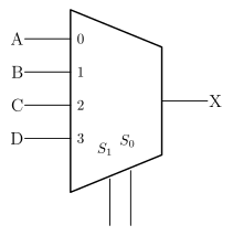
Figure 4: Question 12’s 4-to-1 multiplexer: data inputs A, B, C, D on lines 0 to 3, select lines \(S_1\) and \(S_0\), and output X.
A=1 B=\(G\) C=1 D=\(\bar{G}\)
A=\(G\) B=\(\bar{G}\) C=1 D=1
A=\(\bar{G}\) B=1 C=\(G\) D=1
A=\(G\) B=1 C=\(\bar{G}\) D=1
None of the above
TipAnswer
(d)
A 4-to-1 multiplexer passes input \(S_1S_0\) through to the output, so each data input only has to be right for its own select combination. Substitute each combination into the target function and see what is left, treating \(G\) as an ordinary variable rather than a select line:
| \(S_1\) | \(S_0\) | selected input | \(X = S_0 + (S_1 \oplus G)\) | so the input must be |
|---|---|---|---|---|
| 0 | 0 | A | \(0 + (0 \oplus G) = G\) | \(G\) |
| 0 | 1 | B | \(1 + \ldots = 1\) | 1 |
| 1 | 0 | C | \(0 + (1 \oplus G) = \bar{G}\) | \(\bar{G}\) |
| 1 | 1 | D | \(1 + \ldots = 1\) | 1 |
So A=\(G\), B=1, C=\(\bar{G}\), D=1 — option (d). The two rows with \(S_0 = 1\) are constants because the OR is already satisfied, and the two with \(S_0 = 0\) reduce to \(S_1 \oplus G\) evaluated at that value of \(S_1\). See combinational-logic-blocks.
Q13 — Two’s complement addition
What is the result of adding the 6-bit two’s complement numbers 101111 and 101001?
010000
010111
011000
111000
None of the above
TipAnswer
(c)
Addition in two’s complement is plain binary addition with the carry out of the top bit discarded:
\[\begin{array}{r} 101111 \\ +\; 101001 \\ \hline 1\,011000 \end{array}\]
Column by column from the right: \(1+1 = 0\) carry 1; \(1+0+1 = 0\) carry 1; \(1+0+1 = 0\) carry 1; \(1+1+1 = 1\) carry 1; \(0+0+1 = 1\); \(1+1 = 0\) carry 1 out of the word. Keeping six bits gives 011000.
It is worth noticing that this result is wrong as arithmetic: \(101111\) is \(-17\) and \(101001\) is \(-23\), so the true sum is \(-40\), which does not fit in the range \(-32\) to \(31\). Two negatives have produced a positive result (\(011000 = +24\)), which is the overflow signature. The question asks only what the adder produces, and that is (c). See binary-number-representations.
Q14 — D flip-flop timing
Consider the flip-flop circuit shown below and the associated CLK and output (Q) signals. Which timing diagram shows input (A) values over time which would have resulted in the given output (Q).
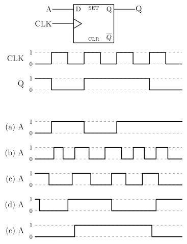
Figure 5: Question 14’s positive-edge-triggered D flip-flop, the given CLK and Q waveforms, and the five candidate A waveforms.
TipAnswer
(b)
The flip-flop is positive-edge triggered (the wedge on the clock input, with no bubble), so Q takes the value A had just before each rising edge of CLK, and holds it until the next one. There are four rising edges. Reading Q:
| rising edge | Q before | Q after | so A must have been |
|---|---|---|---|
| 1st | 1 | 0 | 0 |
| 2nd | 0 | 1 | 1 |
| 3rd | 1 | 1 | 1 |
| 4th | 1 | 0 | 0 |
So the required pattern of A, sampled at the four rising edges, is 0, 1, 1, 0. Checking each candidate at those four instants:
- (a) 0, 1, 0, — : fails at the third edge, where Q stays high but A has just gone low. Note also that (a) changes exactly on the clock edges, which is what a real design goes out of its way to avoid.
- (b) 0, 1, 1, 0 ✓ — and every one of its transitions sits comfortably away from an edge, so there is no ambiguity about which value is sampled.
- (c) 0, 1, 1, 1 : fails at the fourth edge, where Q falls but A is still high.
- (d) 0, 1, 0, 1 : fails at the third and fourth edges.
- (e) 0, 1, 1, 1 : the single wide pulse is still high at the fourth edge, so Q would not fall.
The third edge is the interesting one — Q does not change there, which does not mean A was ignored; it means A happened to equal the value already stored. See flip-flops-and-latches and timing-diagrams.
Q15 — NOR SR latch behaviour
Which truth table correctly captures the behaviour of the following latch circuit?
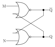
Figure 6: Question 15’s cross-coupled NOR latch. The top gate takes M and the Q feedback and drives \(\overline{Q}\); the bottom gate takes N and the \(\overline{Q}\) feedback and drives Q.
| M | N | Q | \(\overline{Q}\) | |
|---|---|---|---|---|
| (a) | 0 | 0 | Q | \(\overline{Q}\) |
| 0 | 1 | 1 | 0 | |
| 1 | 0 | 0 | 1 | |
| 1 | 1 | 0 | 0 | |
| (b) | 0 | 0 | Q | \(\overline{Q}\) |
| 0 | 1 | 0 | 1 | |
| 1 | 0 | 1 | 0 | |
| 1 | 1 | 1 | 1 | |
| (c) | 0 | 0 | Q | \(\overline{Q}\) |
| 0 | 1 | 0 | 1 | |
| 1 | 0 | 1 | 0 | |
| 1 | 1 | 0 | 0 | |
| (d) | 0 | 0 | 0 | 0 |
| 0 | 1 | 1 | 0 | |
| 1 | 0 | 0 | 1 | |
| 1 | 1 | Q | \(\overline{Q}\) |
- None of the above
TipAnswer
(c)
This is the standard cross-coupled NOR SR latch, with M in the set position and N in the reset position. A NOR outputs 1 only when both its inputs are 0, so any input driven to 1 forces that gate’s output to 0 regardless of the feedback — which is what makes the analysis easy.
- M=1, N=0. The top NOR sees a 1, so \(\overline{Q} = 0\). The bottom NOR then sees \(0\) and \(0\), so \(Q = 1\). Set.
- M=0, N=1. The bottom NOR sees a 1, so \(Q = 0\). The top NOR then sees \(0\) and \(0\), so \(\overline{Q} = 1\). Reset.
- M=0, N=0. Neither gate is forced. Each output feeds the other’s input, so whichever state the latch was already in satisfies both gates and persists. Hold.
- M=1, N=1. Both gates are forced, so \(Q = 0\) and \(\overline{Q} = 0\). The two outputs are no longer complementary — this is the forbidden combination, and it is why the pair of names Q and \(\overline{Q}\) stops being honest here.
That gives hold, reset, set, 0 0 — option (c). Option (a) has set and reset swapped; (b) puts 1 1 in the forbidden row, which is what a NAND latch would do; (d) puts the hold row in the wrong place entirely. See flip-flops-and-latches.
Q16 — Shift register with function select
Which of the following statements about this shift register circuit is false?
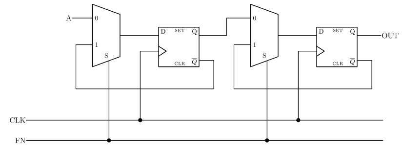
Figure 7: Question 16’s two-stage register. Each stage is a 2-to-1 multiplexer feeding a D flip-flop; input 1 of each multiplexer is that stage’s own \(\overline{Q}\), so FN=1 makes both flip-flops toggle.
If FN is 0, the value of A will be transferred to OUT after two rising clock edges
If FN is 1, OUT will toggle on each rising clock edge
If FN is 0, data is shifted to the right on each rising clock edge
If FN is 1, the value of A is irrelevant
All of the above are true
TipAnswer
(e)
Trace what FN selects. Each multiplexer’s input 0 is the data coming from the left (A for the first stage, the first flip-flop’s Q for the second), and each input 1 is a feedback wire from that same stage’s own \(\overline{Q}\). FN drives both select lines together, so:
- FN = 0 — every flip-flop’s D is the value to its left: \(D_1 = A\) and \(D_2 = Q_1\). That is a two-bit shift register.
- FN = 1 — every flip-flop’s D is its own \(\overline{Q}\), so each one inverts itself on every rising edge. That is a toggle, and the A input is disconnected from the datapath entirely.
Now each statement:
- (a) With FN=0, A is clocked into the first flip-flop on one edge and out to OUT on the next — two rising edges. True.
- (b) With FN=1, \(D_2 = \overline{Q_2}\), so OUT toggles every rising edge. True.
- (c) Data moves from A through the first stage to the second, which is left-to-right as drawn. True.
- (d) With FN=1 both multiplexers select input 1, so A reaches nothing. True.
Nothing among (a) to (d) is false, so the answer is the option that says so: (e). See shift-registers.
The wording is a little awkward — the question asks which statement is false, and (e) is not itself a candidate false statement but a summary of the other four. Selecting it is the paper’s way of saying “none of them is false”.
Q17 — Synchronous counter sequence
What sequence will the following synchronous counter count through, if it starts at \(Q_1Q_0 = 00\)?
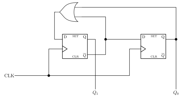
Figure 8: Question 17’s two-flip-flop synchronous counter. The OR gate is drawn mirrored, as on the paper: its output faces left into the first flip-flop’s D input, and its two inputs are fed from \(Q_0\) and \(\overline{Q_1}\).
\(Q_1Q_0\): 00 → 01 → 11 → 10 → 10 → …
\(Q_1Q_0\): 00 → 01 → 11 → 00 → …
\(Q_1Q_0\): 00 → 11 → 01 → 00 → …
\(Q_1Q_0\): 00 → 11 → 10 → 00 → …
None of the above
TipAnswer
(d)
First read the excitation equations off the schematic. The left flip-flop holds \(Q_1\) (its Q output runs down to the \(Q_1\) label) and the right one holds \(Q_0\). The left flip-flop’s \(\overline{Q}\) output is the wire that goes right and then splits: it feeds the second flip-flop’s D input and, going up, one input of the OR gate. The OR gate’s other input comes from the long wire across the top, which runs to the \(Q_0\) node. The OR gate’s output goes back left into the first flip-flop’s D. So:
\[D_1 = Q_0 + \overline{Q_1} \qquad\qquad D_0 = \overline{Q_1}\]
Both flip-flops share one clock, so both D values are computed from the present state and land together on the edge. Tabulating:
| \(Q_1 Q_0\) | \(\overline{Q_1}\) | \(D_1 = Q_0 + \overline{Q_1}\) | \(D_0 = \overline{Q_1}\) | next \(Q_1Q_0\) |
|---|---|---|---|---|
| 0 0 | 1 | 1 | 1 | 1 1 |
| 1 1 | 0 | 1 | 0 | 1 0 |
| 1 0 | 0 | 0 | 0 | 0 0 |
| 0 1 | 1 | 1 | 1 | 1 1 |
Starting from 00 the sequence is \(00 \to 11 \to 10 \to 00 \to \dots\), a three-state cycle — option (d). The fourth row shows the unused state 01 drops into the cycle on the next edge, so the counter cannot lock up outside it.
The mirrored OR gate is the thing to get right when reading the paper’s drawing: the single wire on its pointed left-hand side is the output, and the two wires on its curved right-hand side are the inputs. See counters and sequential-circuits.
Q18 — Overflow detection
Which of the following operations will result in an overflow in 4-bit two’s complement arithmetic?
0111+0111
1111+1111
1010+0110
All of the above result in overflow
None of the above
TipAnswer
(a)
The rule for two’s complement is that overflow happens only when both operands have the same sign and the result has the other one. Adding numbers of opposite signs can never overflow, because the result lies between them. Four bits cover \(-8\) to \(+7\).
- (a) \(0111 + 0111 = 7 + 7 = 14\). In binary \(0111 + 0111 = 1110\), which reads as \(-2\). Two positives gave a negative: overflow.
- (b) \(1111 + 1111 = (-1) + (-1) = -2\). In binary \(1111 + 1111 = 1\,1110\); discarding the carry out leaves \(1110 = -2\) ✓. Two negatives gave a negative, and \(-2\) is in range: no overflow. The carry out of the top bit is not itself overflow.
- (c) \(1010 + 0110 = (-6) + 6 = 0\). In binary \(1010 + 0110 = 1\,0000 \to 0000\) ✓. Opposite signs, so it cannot overflow: no overflow.
Only (a) overflows, so (d) and (e) are both out. See binary-number-representations, and Beyond the paper below for the gate circuit that decides this same question from the sign bits alone.
Q19 — Overflow in a signed addition
Consider the binary addition operation 1011 + 1111. Which of the following statements is true if the numbers are interpreted as two’s complement?
The result is negative and no overflow occurs
The result should be negative but overflow occurs
The result is positive and no overflow occurs
The result should be positive but overflow occurs
The result is zero
TipAnswer
(a)
Decode both operands. \(1011\): invert and add one gives \(0100 + 1 = 0101 = 5\), so \(1011 = -5\). \(1111\): invert and add one gives \(0000 + 1 = 0001\), so \(1111 = -1\). The true sum is \(-6\), which is comfortably inside the 4-bit range \(-8\) to \(+7\), so no overflow is possible.
Doing the addition:
\[\begin{array}{r} 1011 \\ +\; 1111 \\ \hline 1\,1010 \end{array}\]
Discarding the carry out leaves \(1010\), which decodes as \(-(0101 + 1) = -6\) ✓ — negative, correct, and matching the sign of both operands, which is the overflow test passing.
The carry out of the most significant bit is 1 here, and that is the trap: in two’s complement a carry out is normal and is simply discarded. Overflow is a sign condition, not a carry condition. See binary-number-representations — and Beyond the paper below, where the carry-based rule \(V = C_3 \oplus C_4\) has to be rewritten because a real 4-bit adder chip never brings \(C_3\) out to a pin.
Q20 — State table to state diagram
Consider the following state table:
| Current State | Next State (A=0) | Next State (A=1) | Outputs (X,Y) |
|---|---|---|---|
| SA | SA | SB | 0 0 |
| SB | SA | SC | 0 0 |
| SC | SA | SD | 0 1 |
| SD | SD | SE | 1 0 |
| SE | SA | SE | 1 1 |
Which of the following state diagrams is an equivalent representation of this state table? (Input: A, Outputs: XY)
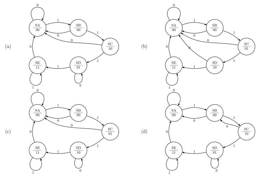
Figure 9: Question 20’s four candidate state diagrams, laid out (a) to (d) as on the paper. Option (e) is None of the above.
- None of the above
TipAnswer
(c)
Check the two things the table specifies — the output written under each state name, and where each of the two arrows out of each state goes.
Outputs. The table gives SA=00, SB=00, SC=01, SD=10, SE=11. Options (a) and (d) both label SC as 10 and SD as 01, i.e. the two are swapped, so both are out immediately. That leaves (b) and (c), which have the outputs right.
Transitions. The table’s five rows are: SA self-loops on 0 and goes to SB on 1; SB returns to SA on 0 and goes to SC on 1; SC returns to SA on 0 and goes to SD on 1; SD self-loops on 0 and goes to SE on 1; SE returns to SA on 0 and self-loops on 1.
Diagram (b) has SD’s 0-transition going back to SA rather than staying in SD, which contradicts the SD row. Diagram (c) has the self-loop on SD, and matches every other row as well, so (c) is the answer.
Worth checking completeness while you are there: each state in (c) has exactly two arrows out, one labelled 0 and one labelled 1, which is what a one-input machine needs — no missing case and no ambiguity. See state-machines.
Q21 — Flip-flops needed for a machine
Consider the state machine represented by the state table in question 20 above (see Q20). What is the minimum number of flip-flops needed to implement this state machine?
2
3
4
5
7
TipAnswer
(b)
\(N\) flip-flops hold \(N\) bits, so they can encode at most \(2^N\) distinct states. The machine has five states (SA to SE), so the requirement is
\[2^N \ge 5 \quad\Rightarrow\quad N \ge \log_2 5 = 2.32\ldots \quad\Rightarrow\quad N = \lceil \log_2 5 \rceil = 3\]
Two flip-flops give only four codes, one short. Three give eight, so five states fit with three codes left unused.
The distractors are the two other plausible counting rules: (d) 5 is one flip-flop per state, which is the one-hot encoding — legal, and often the one that makes the combinational logic simplest, but not the minimum. (c) 4 and (e) 7 do not correspond to anything. See state-machines for the encoding choices.
Q22 — Tracing a state machine
Consider the state machine represented by the state diagram below:
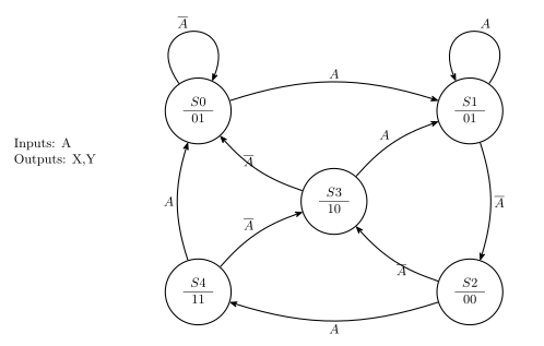
Figure 10: Question 22’s state machine: one input A, outputs X and Y, and five states each with an A and an \(\overline{A}\) transition.
What sequence of states is traversed if the machine starts in state S0 and A goes through the sequence 11110000 (i.e. four 1’s followed by four 0’s)?
S0→S1→S1→S1→S1→S2→S3→S0→S0
S0→S1→S3→S1→S3→S0→S0→S0→S0
S0→S1→S1→S1→S2→S3→S2→S0→S0
S0→S1→S1→S1→S1→S2→S4→S3→S0
None of the above
TipAnswer
(a)
Read the transitions off the diagram first:
| State | on \(\overline{A}\) (0) | on \(A\) (1) |
|---|---|---|
| S0 | S0 (self-loop) | S1 |
| S1 | S2 | S1 (self-loop) |
| S2 | S3 | S4 |
| S3 | S0 | S1 |
| S4 | S3 | S0 |
Now walk the eight inputs from S0, one clock edge per input:
| step | input | from | to |
|---|---|---|---|
| 1 | 1 | S0 | S1 |
| 2 | 1 | S1 | S1 |
| 3 | 1 | S1 | S1 |
| 4 | 1 | S1 | S1 |
| 5 | 0 | S1 | S2 |
| 6 | 0 | S2 | S3 |
| 7 | 0 | S3 | S0 |
| 8 | 0 | S0 | S0 |
Including the starting state, that is S0→S1→S1→S1→S1→S2→S3→S0→S0 — nine entries for a start state plus eight inputs, which is option (a). Note that each of the listed options has nine entries, so the count itself is not a discriminator here; the run of self-loops on S1 while A stays at 1, and the fact that S0 self-loops once the input has gone to 0 and the machine has come home, are what pick (a) out. See state-machines.
Q23 — ALU control for NOR
Consider the ALU bit slice below (not the same as seen previously).
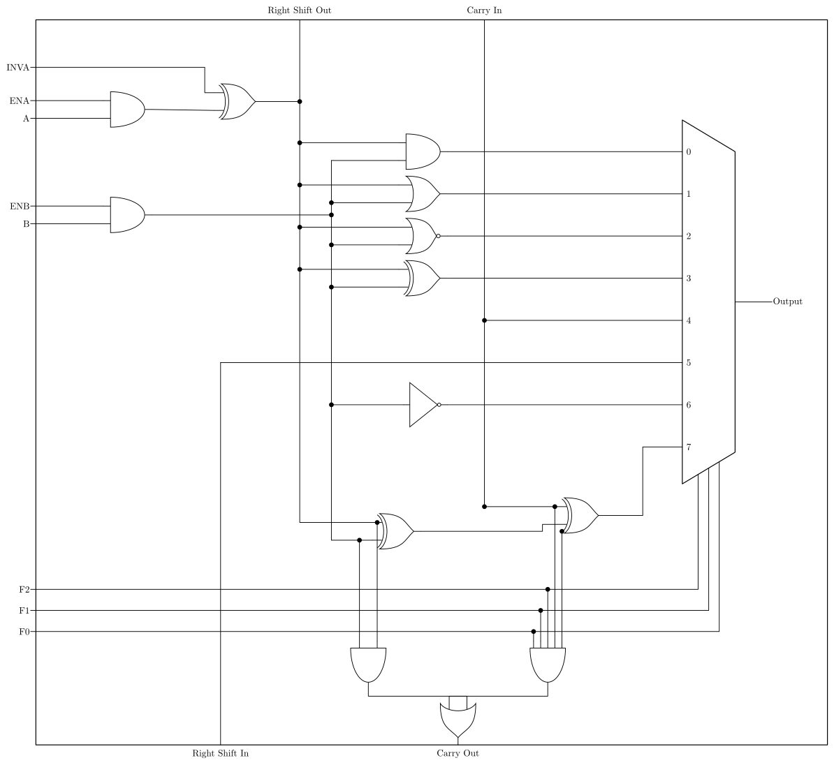
Figure 11: Question 23’s ALU bit slice. The gates at the left condition A and B into the internal signals routed on the two vertical rails; the eight function blocks compute in parallel; the 8-to-1 multiplexer picks one under F2 F1 F0. Carry out is the AND of the two conditioned inputs, ORed with a propagate term gated by the function select.
For an ALU made up of 8 of the bit slices above, which of the following control input settings will result in the ALU output being \(\overline{A + B}\) (bitwise)? (The “Right Shift In” control input refers to that for the most significant bit; the “Carry in” control input refers to that for the least significant bit.)
ENA=1 ENB=1 INVA=0 F2=0 F1=0 F0=1 Right Shift In=1 Carry in=1
ENA=1 ENB=1 INVA=0 F2=0 F1=1 F0=0 Right Shift In=1 Carry in=1
ENA=1 ENB=1 INVA=1 F2=0 F1=0 F0=1 Right Shift In=1 Carry in=1
ENA=1 ENB=1 INVA=1 F2=0 F1=1 F0=0 Right Shift In=1 Carry in=1
None of the above
TipAnswer
(b)
Read the slice in two halves, exactly as in arithmetic-logic-unit.
Input conditioning. The left-hand gates produce two internal signals:
\[X = (A \cdot \text{ENA}) \oplus \text{INVA} \qquad\qquad Y = B \cdot \text{ENB}\]
These are what every function block actually sees. \(X\) is also what leaves the slice as Right Shift Out.
Function select. \(F_2 F_1 F_0\) is the select code of the 8-to-1 multiplexer, so reading the blocks down the middle of the drawing from the top:
| \(F_2 F_1 F_0\) | mux input | Output |
|---|---|---|
| 000 | 0 | \(X \cdot Y\) |
| 001 | 1 | \(X + Y\) |
| 010 | 2 | \(\overline{X + Y}\) |
| 011 | 3 | \(X \oplus Y\) |
| 100 | 4 | Carry In |
| 101 | 5 | Right Shift In |
| 110 | 6 | \(\overline{Y}\) |
| 111 | 7 | \(X \oplus Y \oplus C_{in}\) (the sum) |
The target is \(\overline{A + B}\), a bitwise NOR. So the conditioning must pass both operands through untouched — ENA=1, INVA=0 gives \(X = A\), and ENB=1 gives \(Y = B\) — and the select must pick the NOR block, which is \(F_2F_1F_0 = 010\).
That is option (b). Checking the others: (a) selects 001, the plain OR, giving \(A + B\) rather than its complement; (c) selects 001 with INVA=1, giving \(\overline{A} + B\); (d) has the right select but INVA=1, so it computes \(\overline{\overline{A} + B}\). The Right Shift In and Carry in values are irrelevant once a purely logical function is selected, which is why all four options can share them.
Q24 — ALU control for NOT B
For an ALU made up of 8 of the bit slices shown in question 23 above (see Q23), which of the following control input settings will NOT result in the ALU output being \(\overline{B}\) (bitwise)?
ENA=0 ENB=1 INVA=0 F2=0 F1=1 F0=0 Right Shift In=0 Carry in=0
ENA=0 ENB=1 INVA=1 F2=0 F1=1 F0=1 Right Shift In=0 Carry in=0
ENA=0 ENB=1 INVA=1 F2=1 F1=1 F0=0 Right Shift In=0 Carry in=0
ENA=0 ENB=1 INVA=1 F2=1 F1=1 F0=1 Right Shift In=0 Carry in=0
All of the above result in the ALU output being \(\overline{B}\) (bitwise)
TipAnswer
(d)
Every option has ENA=0 and ENB=1, so from the conditioning equations in Q23:
\[X = (A \cdot 0) \oplus \text{INVA} = \text{INVA} \qquad\qquad Y = B\]
That is, the A side is forced to a constant — all zeros when INVA=0, all ones when INVA=1 — and the B side passes through. Now take each option’s select code:
- (a) 010 selects \(\overline{X + Y}\). With INVA=0, \(X\) is all zeros, and \(\overline{0 + B} = \overline{B}\) ✓.
- (b) 011 selects \(X \oplus Y\). With INVA=1, \(X\) is all ones, and \(1 \oplus B = \overline{B}\) ✓. This is the “XOR with all ones inverts” trick.
- (c) 110 selects \(\overline{Y} = \overline{B}\) ✓. INVA does not matter here, because the inverter block never looks at \(X\).
- (d) 111 selects the adder: \(X \oplus Y \oplus C_{in}\), with the carry rippling from slice to slice. With \(X\) all ones and the external carry in 0, the machine computes \((-1) + B\), i.e. \(B - 1\) — not \(\overline{B}\).
So (d) is the odd one out. The distinction between (b) and (d) is the whole point of the question: mux input 3 is a bitwise XOR with no carry involved, so it really does produce \(\overline{B}\), whereas mux input 7 is the same XOR plus the carry chain, and once carries propagate the result is arithmetic rather than bitwise. Adding all-ones to \(B\) decrements it; only \(B = 0\) (and, in eight bits, \(B = -128\)) happens to satisfy \(B - 1 = \overline{B}\).
The question does not depend on which way round the select bits go, which is a small mercy. The four codes offered are 010, 011, 110 and 111; reversing the bit order maps that set onto itself, swapping (b) and (c) with each other and leaving (a) and (d) where they are. So (d) is still the only failure if \(F_0\) is read as the most significant bit — the answer is the same either way. See arithmetic-logic-unit.
Q25 — Half adder from multiplexers
Consider the half-adder shown below:
In the multiplexer circuit below, what values do the multiplexer inputs X0,X1,X2,X3 and Y0,Y1,Y2,Y3 need to take on in order for the circuit to implement a half-adder?
(Both drawings the question refers to are combined into Figure 12: the half-adder block on top, the two multiplexers underneath.)
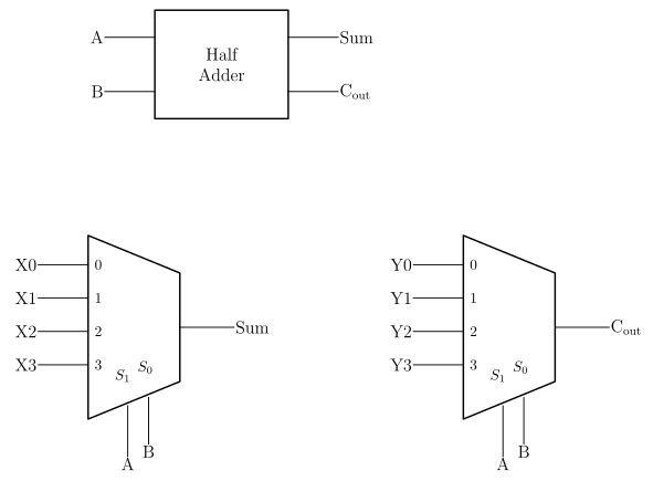
Figure 12: Question 25’s half adder block and the pair of 4-to-1 multiplexers meant to implement it, one for Sum and one for \(C_{out}\), both selected by A and B.
| X0 | X1 | X2 | X3 | Y0 | Y1 | Y2 | Y3 | ||
|---|---|---|---|---|---|---|---|---|---|
| (a) | 0 | 0 | 0 | 1 | 0 | 1 | 1 | 0 | |
| (b) | 0 | 1 | 1 | 0 | 0 | 0 | 1 | 1 | |
| (c) | 0 | 1 | 1 | 0 | 0 | 0 | 0 | 1 | |
| (d) | 0 | 1 | 1 | 0 | 1 | 0 | 0 | 0 |
- None of the above
TipAnswer
(c)
A half adder is just the truth table of two bits added:
| A | B | Sum \(= A \oplus B\) | \(C_{out} = A \cdot B\) |
|---|---|---|---|
| 0 | 0 | 0 | 0 |
| 0 | 1 | 1 | 0 |
| 1 | 0 | 1 | 0 |
| 1 | 1 | 0 | 1 |
Both multiplexers are selected by the same pair of lines, with A on \(S_1\) and B on \(S_0\), so input \(n\) of each multiplexer is the one reached when \(AB\) is the two-bit number \(n\): input 0 for \(AB = 00\), input 1 for \(01\), input 2 for \(10\), input 3 for \(11\). Using a multiplexer this way turns it into a direct lookup of a truth table — the data inputs are the output column, in row order.
Reading the Sum column down gives \(X_0X_1X_2X_3 = 0, 1, 1, 0\), and reading the \(C_{out}\) column gives \(Y_0Y_1Y_2Y_3 = 0, 0, 0, 1\). That is option (c).
The distractors are the same two columns misassigned: (a) has them swapped between the two multiplexers, (b) has \(C_{out}\) set for \(AB = 10\) as well as \(11\), and (d) has the \(C_{out}\) column reversed. See combinational-logic-blocks.
Beyond the paper — building the overflow detector
Q18 and Q19 are both answered on paper the same way: decode the operands into decimal, look at the signs, decide. Learning Lab 3 (Binary Arithmetic) asks the same question the way hardware has to answer it — with gates, on a real adder chip, where nothing is in decimal and not every carry is even visible.
This is the extension to Task 2 of Learning Lab 3 (Binary Arithmetic). Both circuits below are derived from the constraint and checked against the truth table. week2-lab-binary-arithmetic covers the rest of that lab.
The constraint the chip imposes
Task 2 of the lab builds a 4-bit adder from a 74HCT283 — a single 16-pin part holding four full adders with the intermediate carries \(C_1\), \(C_2\) and \(C_3\) wired stage to stage inside the package, so only \(C_0\) (carry in) and \(C_4\) (carry out) come out on pins. See device-pinouts for the pinout and symbol.
The rule Q19’s answer appeals to is usually written in terms of the carries around the sign bit:
\[V = C_3 \oplus C_4\]
— overflow exactly when the carry into the sign column differs from the carry out of it. The lab’s extension task kills that formula in one line: “you don’t have access to C3 which is an internal signal. Therefore, you need the overflow output expressed in terms of available information (i.e. A3, B3, S3, C4).”
So the detector has to be built from the sign bit of each operand, the sign bit of the result, and the carry out.
Two detectors that use only pins
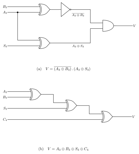
Figure 13: Two gate-level answers to Lab 3’s extension task, both using only signals the 74HCT283 brings out to pins. (a) compares signs directly: the inverted XOR is true when the two operands agree in sign, the second XOR is true when the result disagrees with them, and overflow is the AND of the two. (b) rebuilds the hidden carry: since stage 3 is a full adder, \(C_3 = A_3 \oplus B_3 \oplus S_3\), so the textbook \(V = C_3 \oplus C_4\) becomes a chain of three XORs. Both are derived here — the lab poses the task and gives no solution.
(a) compares signs directly. Overflow means the two operands agreed in sign and the answer came out with the other one, which as a sum of products is
\[V = A_3 B_3 \overline{S_3} + \overline{A_3}\,\overline{B_3}\,S_3 = \overline{(A_3 \oplus B_3)} \cdot (A_3 \oplus S_3)\]
(b) rebuilds the carry the chip hid. Stage 3 is a full adder, so \(S_3 = A_3 \oplus B_3 \oplus C_3\); XOR is its own inverse, so \(C_3 = A_3 \oplus B_3 \oplus S_3\). Substituting into \(V = C_3 \oplus C_4\):
\[V = A_3 \oplus B_3 \oplus S_3 \oplus C_4\]
That is why \(C_4\) is listed among the available signals: it is the only one of the four that (a) does not use, and its presence in the list is the hint that a carry-based answer exists.
Form (b) is the one to build. Its three gates are all the same type, so they come out of one 74HCT86 with a gate spare; form (a) as drawn mixes three types and so needs three packages. (Form (a) can be squeezed onto fewer, since an XOR with one input tied to logic high is an inverter and the pinout sheet gives a symbol for logic high — but it is still four gates against three, and two chips against one.) See device-pinouts for the parts and circuit-schematics for what turns either of these logic diagrams into a buildable schematic.
Checking both against the truth table
\(C_3\) and \(C_4\) below are what the top stage of the adder must have been doing for that combination of \(A_3\), \(B_3\) and \(S_3\) (\(C_3 = A_3 \oplus B_3 \oplus S_3\), and \(C_4\) is the majority of \(A_3\), \(B_3\) and \(C_3\)):
| \(A_3\) | \(B_3\) | \(S_3\) | \(C_3\) | \(C_4\) | \(V\) |
|---|---|---|---|---|---|
| 0 | 0 | 0 | 0 | 0 | 0 |
| 0 | 0 | 1 | 1 | 0 | 1 |
| 0 | 1 | 0 | 1 | 1 | 0 |
| 0 | 1 | 1 | 0 | 0 | 0 |
| 1 | 0 | 0 | 1 | 1 | 0 |
| 1 | 0 | 1 | 0 | 0 | 0 |
| 1 | 1 | 0 | 0 | 1 | 1 |
| 1 | 1 | 1 | 1 | 1 | 0 |
\(V\) is 1 in exactly two rows — two positives giving a negative, and two negatives giving a positive — which is the rule Q18 applies by hand. Both expressions reproduce that column.
The detector reproduces the paper answers
Run the four sign patterns from Q18 and Q19 through the table. Only the top bits matter:
| From | Sum | \(A_3 B_3 S_3\) | \(V\) | Matches |
|---|---|---|---|---|
| Q18 (a) \(0111 + 0111\) | \(1110\) | 0 0 1 | 1 | overflow ✓ |
| Q18 (b) \(1111 + 1111\) | \(1110\) | 1 1 1 | 0 | no overflow, despite \(C_4 = 1\) ✓ |
| Q18 (c) \(1010 + 0110\) | \(0000\) | 1 0 0 | 0 | opposite signs cannot overflow ✓ |
| Q19 \(1011 + 1111\) | \(1010\) | 1 1 1 | 0 | negative, no overflow ✓ |
Row two is the whole point of Q19’s last paragraph, now visible as wiring: \(C_4\) is 1 there, but \(C_4\) is not an input to the sign comparison at all in form (a), and in form (b) it is cancelled by \(C_3\), which is also 1. A carry out is not an overflow — the detector is built so that it cannot confuse the two, which is exactly why the LED for it is a separate output from the carry LED. See binary-number-representations and combinational-logic-blocks.
Your score
Reload the page to clear your answers.