Lab 8 — State Machines
Learning Lab 8: two FSM design exercises taken all the way from a state diagram to a Logisim circuit. See state-machines for the notation and the design procedure, and 2026-08-20-state-machines for the lecture.
Method: do the hand design first — state diagram → state table → next state logic and output logic — then implement and test in Logisim. (Also watch the LEC 08 — Example FSM Design 1 & 2 videos on Blackboard.)
Worked: the next Gray code value
0000, 0001, 0011, 0010, …
0110.
Gray code changes exactly one bit between consecutive values. From 0010, the values that differ in one bit are 0011 (already used), 0000 (used), 0110, and 1010. The standard reflected ordering takes 0110 next — after which come 0111, 0101, 0100, 1100, … 1010 is also one bit away, but flipping the most significant bit here breaks the reflection pattern. See binary-number-representations and the encoding table in state-machines.
Design Task 1 — Sequence Detector
Draw a state diagram for a system that detects the sequence 001 in a series of bits.
- Input: S
- Output: X
The output X is 1 whenever the sequence 001 is detected on the input S (i.e. 0 followed by 0 followed by 1).
Example input sequence   S = 00101010010001
Example output sequence  X = 00100000010001
Then:
- Write down a 2-dimensional state table
- Choose a state encoding — state encoding = number of flip-flops and their values in each state. Examine different options for state encoding!
- Write down a 1-dimensional state table using your encoding
- Determine Boolean expressions for the output (X) and the next state (flip-flop inputs, D’s) in terms of the current state (flip-flop outputs, Q’s) and input (S)
- Enter the circuit into Logisim and simulate it
Working — Task 1
State diagram
The state has to remember how much of 001 has been matched so far. That gives four states — and the fourth exists only because this is a Moore machine, so “I have just detected it” must be a state of its own in order to have an output of its own.
| State | Means | X |
|---|---|---|
| \(S_0\) | no useful progress (last bit was a 1, or just started) | 0 |
| \(S_1\) | seen 0 |
0 |
| \(S_2\) | seen 00 |
0 |
| \(S_3\) | just detected 001 |
1 |
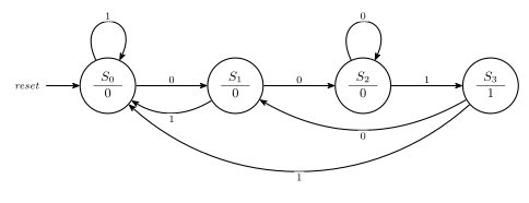
Figure 1: The 001 detector. Every state has two arrows out, one per value of S, which is completeness for a one-input machine. The self-loop on S2 is the important one: a run of three or more zeros stays ready to detect, rather than falling back. From S3 the last bit consumed was a 1, so it behaves exactly like S0 — same transitions, different output.
Each state is a circle divided by a chord, with the name above and the output below. A transition is a plain single-headed arrow, labelled with a bare 0 or 1 for a one-input machine. Two more conventions in the figure above:
- The start state is marked by an incoming reset arrow from nowhere.
- A self-loop is an arrow from a state back to itself. The completeness rule (transition arrows from each state must encompass all possibilities, exactly once) guarantees most machines need them.
See csse2010-diagram-notation for the full list of conventions.
Traced against the example sequence in the task, this machine reproduces the example output exactly; the trace is worked out edge by edge below.
2-dimensional state table
| Current state | Next state (\(\overline{S}\)) | Next state (\(S\)) | X |
|---|---|---|---|
| \(S_0\) | \(S_1\) | \(S_0\) | 0 |
| \(S_1\) | \(S_2\) | \(S_0\) | 0 |
| \(S_2\) | \(S_2\) | \(S_3\) | 0 |
| \(S_3\) | \(S_1\) | \(S_0\) | 1 |
Choosing an encoding
Four states, so two flip-flops. The choice genuinely matters, which is what the instruction to examine different options is getting at.
The obvious assignment \(S_0 = 00\), \(S_1 = 01\), \(S_2 = 10\), \(S_3 = 11\) gives three product terms for \(D_1\) and three more for \(D_0\) — nothing collapses.
Now look at the 2-D table again: the \(\overline{S}\) column and the \(S\) column each contain only two distinct destinations, and on \(S = 1\) every state goes to either \(S_0\) or \(S_3\). If the encoding is arranged so that one flip-flop bit tracks the input directly, that bit’s logic disappears entirely. Assigning
\[S_0 = 01 \qquad S_1 = 00 \qquad S_2 = 10 \qquad S_3 = 11\]
does exactly that.
1-dimensional state table
| State | \(Q_1 Q_0\) | \(S\) | Next state | \(D_1 D_0\) | X |
|---|---|---|---|---|---|
| \(S_0\) | 01 | 0 | \(S_1\) = 00 | 0 0 | 0 |
| \(S_0\) | 01 | 1 | \(S_0\) = 01 | 0 1 | 0 |
| \(S_1\) | 00 | 0 | \(S_2\) = 10 | 1 0 | 0 |
| \(S_1\) | 00 | 1 | \(S_0\) = 01 | 0 1 | 0 |
| \(S_2\) | 10 | 0 | \(S_2\) = 10 | 1 0 | 0 |
| \(S_2\) | 10 | 1 | \(S_3\) = 11 | 1 1 | 0 |
| \(S_3\) | 11 | 0 | \(S_1\) = 00 | 0 0 | 1 |
| \(S_3\) | 11 | 1 | \(S_0\) = 01 | 0 1 | 1 |
Boolean expressions
Reading the \(D_0\) column: it is 1 in exactly the four rows where \(S = 1\), and 0 in the four where \(S = 0\).
\[\boxed{D_0 = S}\]
A direct wire from the input to the flip-flop — no gate at all. Reading \(D_1\), which is 1 at \((Q_1Q_0, S) = (00,0), (10,0), (10,1)\):
\[D_1 = \overline{Q_1}\,\overline{Q_0}\,\overline{S} + Q_1\overline{Q_0}\,\overline{S} + Q_1\overline{Q_0}S = \overline{Q_0}\left[\overline{S}(\overline{Q_1} + Q_1) + Q_1 S\right] = \overline{Q_0}\left[\overline{S} + Q_1 S\right]\]
and by the redundancy (simplification) theorem, \(\overline{S} + Q_1 S = \overline{S} + Q_1\):
\[\boxed{D_1 = \overline{Q_0}\,(Q_1 + \overline{S})}\]
\(X\) is 1 only in \(S_3 = 11\):
\[\boxed{X = Q_1 \cdot Q_0}\]
Checking it, edge by edge
Running the expressions against the sequence the task supplies, one column per clock edge — the state shown is the one the machine is in after that edge, and X is that state’s output:
S       =    0  0  1  0  1  0  1  0  0  1  0  0  0  1
state       S1 S2 S3 S1 S0 S1 S0 S1 S2 S3 S1 S2 S2 S3
Q1 Q0       00 10 11 00 01 00 01 00 10 11 00 10 10 11
X       =    0  0  1  0  0  0  0  0  0  1  0  0  0  1
which is X = 00100000010001, the example output sequence in the task, exactly. The three detections land on the final 1 of each 001, including the one at the very end, and the 000 at positions 11–13 shows the self-loop on \(S_2\) doing its job: a third zero keeps the machine ready instead of dropping it back to the start.
The circuit
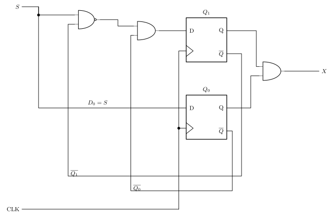
Figure 2: The 001 detector as a logic diagram, the circuit the task’s last bullet asks for (enter the circuit into Logisim and simulate it). Three things the algebra hides are visible here. D0 is a bare wire from the input S to a flip-flop, with no gate anywhere in the path. Both complements the next-state logic needs come off the flip-flops’ own Qbar pins, so the circuit contains no inverter. And the output AND sits to the right of the flip-flops, fed by Q1 and Q0 only - never by S - which is exactly what makes this a Moore machine. The two long return wires at the bottom carry Qbar1 and Qbar0 back to the gates; lines that cross without a junction dot are not connected.
Challenge — the detector in three chips
The challenge is to implement the sequence detector with just three chips: three 74-series packages, total, for Figure 2.
Two D flip-flops are one 74HCT74, leaving two chips for the logic. The trick is that \(\overline{Q_0}\) and \(\overline{Q_1}\) come free from the flip-flops’ complementary outputs, so no inverter package is needed — and De Morgan turns the OR into a NAND that can use \(\overline{Q_1}\) directly:
\[Q_1 + \overline{S} = \overline{\overline{Q_1} \cdot S} \quad\Longrightarrow\quad D_1 = \overline{Q_0} \cdot \operatorname{NAND}(\overline{Q_1},\, S)\]
| Signal | Built from |
|---|---|
| \(D_0 = S\) | a wire |
| \(D_1\) | one NAND + one AND, using \(\overline{Q_0}\) and \(\overline{Q_1}\) from the flip-flops |
| \(X = Q_1 Q_0\) | one AND |
| Chip | Used for |
|---|---|
74HCT74 dual D flip-flop |
\(Q_1\), \(Q_0\) |
74HCT00 quad NAND |
1 gate |
74HCT08 quad AND |
2 gates |
Three chips, with three of the four NAND gates and two of the four AND gates spare. See device-pinouts for the pinouts and circuit-schematics for the drawing rules.
Design Task 2 — Sequence Matching
Consider a sequence matching system with
- 2 inputs A, B
- 2 outputs X, Y
- X is 1 if A and B have been the same value (i.e. both 0 or both 1) twice or more in a row, otherwise 0
- Y is 1 if the A and B values are different, otherwise 0
- Initially the A and B values are assumed to have been different and Y should be 1
Draw a state diagram and discuss with tutoring staff. Implement: write down a 2-D state table, choose a state encoding, write down a 1-D state table, determine Boolean expressions for the outputs and the next state (flip-flop inputs, D’s) in terms of the current state (flip-flop outputs, Q’s) and inputs, and enter the circuit into Logisim and simulate.
Working — Task 2
Reducing the inputs
A and B never matter individually — only whether they agree. Define
\[M = \overline{A \oplus B} \qquad (M = 1 \text{ when } A = B)\]
so the four input combinations collapse to two cases, and 00 behaves identically to 11.
State diagram
The machine must remember how long the current run of matches is, capped at two:
| State | Means | X | Y |
|---|---|---|---|
| \(D\) | the last pair differed — the reset state | 0 | 1 |
| \(M_1\) | matched once (the pair before differed) | 0 | 0 |
| \(M_2\) | matched twice or more in a row | 1 | 0 |
That the reset state is \(D\) with \(Y = 1\) is given by the specification: initially the A and B values are assumed to have been different and Y should be 1.
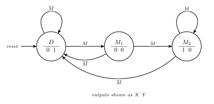
Figure 3: The sequence matcher, with M meaning A equals B. Any mismatch drops straight back to D from anywhere, so the run counter resets in one clock; a match walks D to M1 to M2, where it stays. The two outputs are each true in exactly one state, which is what makes the encoding below collapse the output logic to nothing.
2-dimensional state table
| Current state | \(AB = 00\) (\(M\)) | \(01\) (\(\overline{M}\)) | \(10\) (\(\overline{M}\)) | \(11\) (\(M\)) | X | Y |
|---|---|---|---|---|---|---|
| \(D\) | \(M_1\) | \(D\) | \(D\) | \(M_1\) | 0 | 1 |
| \(M_1\) | \(M_2\) | \(D\) | \(D\) | \(M_2\) | 0 | 0 |
| \(M_2\) | \(M_2\) | \(D\) | \(D\) | \(M_2\) | 1 | 0 |
Choosing an encoding
Three states, so two flip-flops, with one code left over. Each output is true in exactly one state, so if the two flip-flops are made to be the two outputs, the output logic vanishes entirely. Take \(Q_1 = X\) and \(Q_0 = Y\):
\[D = 01 \qquad M_1 = 00 \qquad M_2 = 10 \qquad (11 \text{ unused})\]
\[\boxed{X = Q_1} \qquad \boxed{Y = Q_0}\]
1-dimensional state table
| State | \(Q_1 Q_0\) | \(M\) | Next state | \(D_1 D_0\) | X | Y |
|---|---|---|---|---|---|---|
| \(D\) | 01 | 0 | \(D\) = 01 | 0 1 | 0 | 1 |
| \(D\) | 01 | 1 | \(M_1\) = 00 | 0 0 | 0 | 1 |
| \(M_1\) | 00 | 0 | \(D\) = 01 | 0 1 | 0 | 0 |
| \(M_1\) | 00 | 1 | \(M_2\) = 10 | 1 0 | 0 | 0 |
| \(M_2\) | 10 | 0 | \(D\) = 01 | 0 1 | 1 | 0 |
| \(M_2\) | 10 | 1 | \(M_2\) = 10 | 1 0 | 1 | 0 |
Boolean expressions
\(D_0\) is 1 in exactly the rows where \(M = 0\):
\[\boxed{D_0 = \overline{M} = A \oplus B}\]
\(D_1\) is 1 at \((Q_1Q_0, M) = (00, 1)\) and \((10, 1)\), so \(Q_1\) is a don’t-care:
\[D_1 = \overline{Q_1}\,\overline{Q_0}M + Q_1\overline{Q_0}M = \overline{Q_0}M(\overline{Q_1} + Q_1) \quad\Longrightarrow\quad \boxed{D_1 = \overline{Q_0} \cdot M}\]
Writing \(E = A \oplus B\) so that \(M = \overline{E}\), De Morgan folds \(D_1\) into a single gate:
\[D_1 = \overline{Q_0} \cdot \overline{E} = \overline{Q_0 + E} = \operatorname{NOR}(Q_0,\, A \oplus B)\]
So the whole circuit is one XOR feeding both a flip-flop input and a NOR, with the outputs taken straight off the flip-flops.
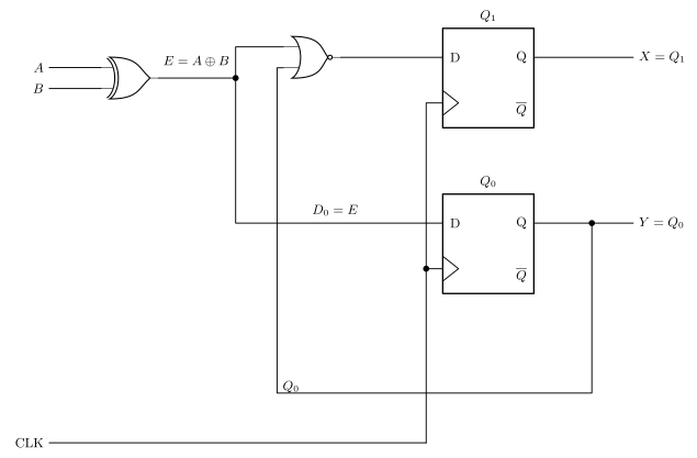
Figure 4: The sequence matcher as a logic diagram. One XOR does all of the input reduction: E = A xor B is simultaneously D0 and one input of the NOR that forms D1. Because the encoding was chosen so that the two flip-flops are the two outputs, X and Y are taken straight off Q1 and Q0 and there is no output logic at all - the entire machine is two gates and two flip-flops. The one feedback wire, Q0 back to the NOR, is the whole of the next-state logic that depends on the state. Lines crossing without a junction dot are not connected.
At chip level that NOR is the awkward part. The course’s parts list has quad NAND, AND, OR and XOR packages plus a hex inverter, but no NOR — see device-pinouts. Rewriting \(D_1 = \overline{Q_0}\cdot\overline{E}\) as an AND of two complements fixes it: \(\overline{Q_0}\) is free from the flip-flop and \(\overline{E}\) is one inverter on the XOR output, giving 74HCT86 + 74HCT04 + 74HCT08 + 74HCT74, four chips.
Checking the unused state
The encoding leaves \(Q_1Q_0 = 11\) unassigned, so it is worth confirming the machine cannot get stuck there (the same lock-up check as week4-lab-lab-7-exercises). Substituting \(Q_1Q_0 = 11\):
\[D_1 = \overline{Q_0}\cdot M = 0 \cdot M = 0 \qquad D_0 = \overline{M}\]
so from 11 the machine goes to 01 (\(D\)) when \(M = 0\), or 00 (\(M_1\)) when \(M = 1\). Both are legal states, so it self-corrects within one clock — no lock-up, and no extra logic needed to guarantee it.
See also
- state-machines · sequential-circuits · flip-flops-and-latches · counters
- 2026-08-20-state-machines — Lecture 8
- circuit-schematics · device-pinouts — for the three-chip challenge
- binary-number-representations — Gray code
- csse2010-diagram-notation — the state-diagram and logic-diagram conventions these figures follow